EP0247739A2 - Semiconductor nonvolatile memory device - Google Patents
Semiconductor nonvolatile memory device Download PDFInfo
- Publication number
- EP0247739A2 EP0247739A2 EP87303875A EP87303875A EP0247739A2 EP 0247739 A2 EP0247739 A2 EP 0247739A2 EP 87303875 A EP87303875 A EP 87303875A EP 87303875 A EP87303875 A EP 87303875A EP 0247739 A2 EP0247739 A2 EP 0247739A2
- Authority
- EP
- European Patent Office
- Prior art keywords
- power source
- memory cell
- voltage
- nonvolatile
- programmable read
- Prior art date
- Legal status (The legal status is an assumption and is not a legal conclusion. Google has not performed a legal analysis and makes no representation as to the accuracy of the status listed.)
- Granted
Links
Images


Classifications
-
- G—PHYSICS
- G11—INFORMATION STORAGE
- G11C—STATIC STORES
- G11C17/00—Read-only memories programmable only once; Semi-permanent stores, e.g. manually-replaceable information cards
-
- G—PHYSICS
- G11—INFORMATION STORAGE
- G11C—STATIC STORES
- G11C14/00—Digital stores characterised by arrangements of cells having volatile and non-volatile storage properties for back-up when the power is down
- G11C14/0054—Digital stores characterised by arrangements of cells having volatile and non-volatile storage properties for back-up when the power is down in which the volatile element is a SRAM cell
- G11C14/0063—Digital stores characterised by arrangements of cells having volatile and non-volatile storage properties for back-up when the power is down in which the volatile element is a SRAM cell and the nonvolatile element is an EEPROM element, e.g. a floating gate or MNOS transistor
-
- G—PHYSICS
- G11—INFORMATION STORAGE
- G11C—STATIC STORES
- G11C5/00—Details of stores covered by group G11C11/00
- G11C5/14—Power supply arrangements, e.g. power down, chip selection or deselection, layout of wirings or power grids, or multiple supply levels
- G11C5/141—Battery and back-up supplies
-
- G—PHYSICS
- G11—INFORMATION STORAGE
- G11C—STATIC STORES
- G11C5/00—Details of stores covered by group G11C11/00
- G11C5/14—Power supply arrangements, e.g. power down, chip selection or deselection, layout of wirings or power grids, or multiple supply levels
- G11C5/143—Detection of memory cassette insertion or removal; Continuity checks of supply or ground lines; Detection of supply variations, interruptions or levels ; Switching between alternative supplies
Definitions
- the present invention relates to a semiconductor nonvolatile memory device. More particularly, the present invention is related to a memory-device in the form of a nonvolatile RAM (NVRAM), in which a volatile memory, for example, a static random access memory for example (SRAM) or dynamic random access memory (DRAM) and / an electrically erasable and programmable read only memory (EEPROM or E2PROM) are combined on a one to one basis.
- NVRAM nonvolatile RAM
- SRAM static random access memory
- DRAM dynamic random access memory
- EEPROM electrically erasable and programmable read only memory
- a memory cell array of an NVRAM is for example composed of a number of memory cell units in which/an SRAM cell and an EEPROM cell are combined, and before the power source is turned OFF, the content of the SRAM cell is transferred to the EEPROM cell, thus rendering the device nonvolatile.
- the SRAM carries out a read/write operation as a conventional SRAM, and before the power source is turned OFF, the data in the SRAM is written into the EEPROM, and utilizing the nonvolatile characteristic, data is held therein while the power source is OFF.
- the power source is again switched ON, the data in the EEPROM is recalled to the SRAM and a conventional read/write operation carried out.
- a store signal ST inverted ST
- a recall signal RC inverted RC
- a nonvolatile enable signal NE (inverted NE) is combined with one of a write enable signal WE (inverted WE), a chip enable signal CE (inverted CE) and an output enable signal OE (inverted OE), to realize either the above-noted store signal mode or recall mode and,therefore, a control pin must be utilized for this procedure.
- An embodiment of the present invention may provide an improved semiconductor nonvolatile memory device in which the use of a specified control signal for the control of a store operation is unnecessary.
- a semiconductor nonvolatile memory device including: a plurality of nonvolatile random access memory cells, each constituted by a volatile memory cell and a nonvolatile erasable programmable read only memory cell a sense circuit / .
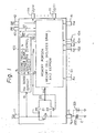
- the device of Fig. 1 includes a semiconductor nonvolatile memory provided with device 100, a power source back-up capacitor 200, N channel MOS transistors 21, 22 and 24, a positive side power source potential level V CC , an auxiliary power source V AUX , a pin terminal 11 for the positive side power source, a pin terminal 12 for the auxiliary power source, a node 23 of a common power source or an inner power source, a sense circuit 13 for sensing the positive side power source potential level V CC , and a switching- over control circuit 14 for generating a store/recall signal and controlling the transistor 22.
- the semiconductor nonvolatile memory device 100 includes address input pin terminals 101 ⁇ 10n receiving address signals A --- A l , A , A ; a pin terminal 41 receiving a negative side power source potential level V SS ; data input/output pin terminals 111 ⁇ 11K receiving input/output data I/O(1) --- I/O(k) ; and a pin terminal 43 receiving a chip select signal CS, a pin terminal 42 receiving a write enable signal WE other than the pin terminals 11 and 12.
- a battery 201 is connected to pin terminals 11 and 12 in place for a capacitor 200, when a transistor 24 is not connected between the terminals 11 and 12.
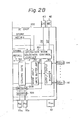
- Fig. 1 The arrangement of the device shown in Fig. 1 is shown in detail in Fig. 2.
- a positive side power source potential Vc is applied to the pin terminal 11 as the positive side power source.
- the positive side power source potential level V CC is applied through the diode-connected transistor 21 as an internal power source V CC ' to memory portion 30, and further applied to the back-up capacitor 200 through the transistor 24 and the auxiliary power source pin terminal 12, voltage V CC is also supplied from the pin terminal 11 to the V CC sense circuit 13.
- the voltage is supplied to each point of the semiconductor nonvolatile memory device from the internal power source, and thus the device can carry out a normal read/write operation.
- a signal for cutting off the transistor 22 is sent from the store/recall & power supply switching control circuit 14, and the power source back-up capacitor 200 is charged through the transistor 24.
- the power source When the power source is turned OFF and the positive side power source potential level V CC , for example 4.5 to 5 volts, is reduced from 3 volts to 2 volts, the variation is detected immediately at the V CC voltage sense circuit 13 at the positive side power source, and a store/recall & power supply switching control circuit 14 then outputs a store signal ST, to transfer the content of a SRAM to an EEPROM.
- a transistor 22 is turned ON and the voltage of the potential level V AUX (nearly equal to 4.5 through 5 volts) from the capacitor 200 is supplied as the internal power source at the node 23, thus backing-up the store operation.
- the transistors 21 and 24 are turned OFF. Responding to the store signal, a write high voltage V HH is produced and a store operation is carried out.
- the potential level V AUX of the power source back-up capacitor 200 is 0 volt at the beginning and the positive side power source potential level V CC is also 0 volt. This potential level then rises gradually, and when the potential level reaches from 3 volts to 4 volts, the positive side power source potential level V CC sense circuit 13 outputs a recall signal, thus transferring the content of the EEPROM to the SRAM. The transfer will be completed by the time the positive side power source potential level V CC reaches 4.5 volts.
- the capacitance of the power source back-up capacitor is determined as follows. Transistor 22 is turned OFF and transistors 21 and 24 are turned ON. Then, in response to a recall signal, an undermentioned transistor T5 is turned ON, the voltages V C1 and V C2 are applied in a predetermined sequence, to carry out a recall operation. Suppose that it takes 10 ms for the store operation and the store operation is finished during the time that the potential level V AUX of the power source back-up capacitor is reduced from 4.5 volts to 4.0 volts, further suppose that the current required for the store operation is 10 milliamperes, then from the expression where i denotes store current and store T time, the capacitance C of the capacitor 201 becomes
- a capacitor having a capacitance of 20 microfarads can handle the above operation, but a capacitor having a capacitance of 100 microfarads can handle all operational requirements.
- a capacitor 200 is connected to a pin 12.
- a lithium battery 201 may be connected thereto. In this case, it is not necessary to connect the transistor 24 thereto for charging up the capacitor 200.
- the memory portion 30 includes an operation mode selection control circuit 301, a booster circuit 302, a timer 303, a bit line load control circuit 304, a memory cell array 305 a decoder 306, an address buffer 307, a decoder 308, an address 309, an output/input buffer 310, a sense ampli- fier/input buffer 311, and a column gate 312.
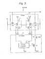
- an SRAM cell 41 is constituted by a flip-flop circuit which includes two P-channel type MOS transistors Tl and T2, two N-channel type MOS transistors T3 and T4 and two channel MOS transistors TW1 and TW2.
- BL and BL denote bit-lines and WL and WL word lines.
- the EEPROM cell 51 i.e., the nonvolatile memory cell, is constituted by a single MOS transistor T6 having a floating gate FG.
- the MOS transistor T5 is used in a recall operation and a recall signal is supplied to a gate thereof.
- a store circuit 52 is a circuit for storing data, and during a store operation, injects positive or negative charges to the floating gate FG of a transistor T6 in response to the "H" or "L" level of nodes Nl and N2. Accordingly, the writing of data to the nonvolatile memory cell transistor T6 is carried out by injecting the charge from the store circuit 52 to the floating gate FG. Therefore, the threshold level of the transistor T6 is changed and the transistor T6 is turned ON or OFF, in accordance with the state of the flip-flop circuit of the SRAM 41.
- separate power sources V C1 and V C2 are provided for the recall operation. Turning transistor T5 ON, an applied timing to the voltages-V C1 and V C2 is postponed to carry out a recall operation.
- V CC voltage sense circuit 13 and the store/recall & power source change-over control circuit 14 as shown in Fig. 2 is shown in detail in Fig. 4.
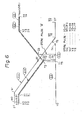
- Examples of the waveforms of the voltages V1, V2, and V3 in the circuit of Fig. 4 are shown in Figs. 5 and 6.
- the external positive side power source voltage V CC is supplied via the pin 11 to the depletion transistors T11 and T13.
- T 12 and T 14 are also depletion type transistors.
- a series connected circuit of T11 and T12, and a series- connected circuit of T 13 and T 14 form a divider circuit, respectively.
- the conductance gm of T 11 and T 12 is designed in such a way that when the voltage V CC exceeds 4V, the output of a buffer B 11 may be inverted.
- the conductance gm of T 13 and T 14 is designed in such a way that when the voltage V CC reduces below 3V, the output of the buffer B21 may be inverted.
- the voltage Vl is fed to a buffer B12 and the output of the buffer B12 is sent, on one side to a NAND gate Gl, and on the other side, to an inverter IV11, and then via a resistor R11 to another terminal of the NAND gate G1, where the multiplication of the resistor R11 and a capacitor C11 produces a time constant C 11 R I1 for generating the recall width.
- the output of a NAND gate Gl is sent on one side to a buffer Bl3 and produces a recall pulse, and on the other side, to a NAND gate G2. Then, the output of the NAND gate G2 is sent to a gate G22 via an inverter IV12 and a buffer B14, to a second input of a NAND gate G22.
- a NAND gate G2 and an inverter IV12 form a latch circuit.
- the output of the NAND gate Gl latches the trailing from an H level to an L level and the output is at an H level. Therefore, after the voltage V CC surfaces 4V, the output V4 of the buffer B14 is kept at an H level.
- a ring oscillator 141 is composed of a NAND gate G22" inverters IV23 and IV24, resistors R22, R23, and R24, and capacitors C22, C23, and C24.
- the output of the ring oscillator 141 is fed back to the gate G22 as a third input.
- the output of the ring oscillator 141 is sent to an inverter 25 and the output of the inverter 25 is, on one side, fed to a second input of a booster circuit 142, and on the other side, to a first input of the booster circuit 142 via an inverter IV26.
- the voltage V CC is boosted from 3 volts to 5 volts and the output of the booster circuit 142 is sent to the transistor 22 as a voltage V SW .
- V AUX > 3 volts.
- the transistor 22 When the voltage of V sw is V AUX and the boosting which makes higher than the value of V AUX is carried out, the transistor 22 can be completely turned ON. As a result, the transistor 22 is turned ON and the voltage of the capacitor 200 is supplied as V CC '
- the output of the gate G21 is sent to an operation mode selection control circuit 301 as a store pulse.
- both the second input of the NAND gate G2 and the output of the inverter IV12, and both the output of the NAND gate G2 and the input of the inverter IV12, are cascade-connected, and further, the resistors R12 are connected to the output of the gate G2 and R13 connected to the output of the inverter IV12 in such a way that when the voltage of the internal power source is V CC ' rises, the voltage V4/kept low until the voltage rises from 0 volt to 4 volts to deactivate a ring oscillator.
- V CC when the power source is switched ON at a point Pl, the voltage V CC is raised from 0 volt to 5 volts via a point of 4 volts P2 and the waveform is flat at points P3 and P4 of:5 volts.
- the voltage of V CC ' is raised from 0 volt to 4.5 through 4.8 volts, the values of which is (V CC -V TH ), that is, a threshold voltage V TH is reduced from a positive side power source voltage V CC .
- the value of V CC' starts from a point Ql to a point Q3 via a point Q2 and reaches the value of (V CC -V TH ) at points Q3 and Q4 .
- the voltage V CC When the voltage V CC is ON, the voltage V CC ' responds to the voltage V CC and the voltage V, responds to the voltage V CC '.
- a corresponding step pulses v is generated to cut out the step waveform of Vl.
- the waveform is traced by points SO, Sl, S2 --- S6 and S7.
- a recall/pulse In response to the generation of Vl, a recall/pulse is generated.
- a store pulse is produced in line with a set of points Z0 and Z7.
- V SW is boosted from 3 volts to 5 volts.
- the potential level of the power source is raised, at the voltage of 4 volts a potential level is set to an H level. Therefore, when the power source is switched ON and the voltage is 3 volts, then a potential level is at a Low state, so the booster circuit 142 does not carry out a boosting operation.
- tracing points of store corresponds to points ZO to Z7, V CC to points WO to W3, V CC ' to points XO to X4, V3 to points YO to Y4 and V2 to points TO to T7.
Abstract
Description
- The present invention relates to a semiconductor nonvolatile memory device. More particularly, the present invention is related to a memory-device in the form of a nonvolatile RAM (NVRAM), in which a volatile memory, for example, a static random access memory for example (SRAM) or dynamic random access memory (DRAM) and/an electrically erasable and programmable read only memory (EEPROM or E2PROM) are combined on a one to one basis.
- In general, a memory cell array of an NVRAM is for example composed of a number of memory cell units in which/an SRAM cell and an EEPROM cell are combined, and before the power source is turned OFF, the content of the SRAM cell is transferred to the EEPROM cell, thus rendering the device nonvolatile.
- That is, when the power source is ON, the SRAM carries out a read/write operation as a conventional SRAM, and before the power source is turned OFF, the data in the SRAM is written into the EEPROM, and utilizing the nonvolatile characteristic, data is held therein while the power source is OFF. When the power source is again switched ON, the data in the EEPROM is recalled to the SRAM and a conventional read/write operation carried out.
- To control such a type of NVRAM, the. following method is utilized.
- For example, when two sorts of signals, i.e., a store signal ST (inverted ST) and a recall signal
RC (inverted RC), are used, and a store signal ST falls to a LOW level, the content of the SRAM is transferred to the EEPROM. Conversely, when a recall signal RC falls to a LOW level, the content of the EEPROM is transferred to the SRAM. - A nonvolatile enable signal NE (inverted NE) is combined with one of a write enable signal WE (inverted WE), a chip enable signal CE (inverted CE) and an output enable signal OE (inverted OE), to realize either the above-noted store signal mode or recall mode and,therefore, a control pin must be utilized for this procedure.
- An embodiment of the present inventionmay provide an improved semiconductor nonvolatile memory device in which the use of a specified control signal for the control of a store operation is unnecessary.
- Therefore, in accordance with the present invention, there is provided a semiconductor nonvolatile memory device including: a plurality of nonvolatile random access memory cells, each constituted by a volatile memory cell and a nonvolatile erasable programmable read only memory cell a sense circuit / . sense the level-of the potential of a power source, and based on the sensed level, to select a store operation or a recall operation; receiving and a first terminal for receiving the power source and a second receiving in use, terminal for receiving an auxiliary power source; wherein in use the detection of a rise or fall of the potential at the first terminal is carried out in the sense circuit, and based on the result of the potential detection, a data transmission from the volatile random access memory cell to the nonvolatile erasable programmable read only memory cell, or from the nonvolatile erasable programmable read only memory cell to the volatile random access memory celJ is automatically carried out.
- Reference is made, by way of example, to the accompanying drawings,
- Figure 1 is a block diagram of the fundamental structure of a semiconductor nonvolatile memory device according to an embodiment of the present invention;
- Fig. 2 shows the arrangement of the device of Fig. 1 in detail;
- Fig. 3 is a circuit diagram of the structure of the NVRAM cell EEPROM in the device of Fig. 1;
- Fig. 4 is a circuit diagram of the VCC voltage sense circuit and the store/recall & power supply switching control circuit in the device of Fig. 1; and,
- Fig. 5 and Fig. 6 are line diagrams showing the generation of a recall pulse and a store pulse, respectively.
- A fundamental structure of a semiconductor nonvolatile memory device according to an embodiment of the present invention is shown in Fig. 1. The device of Fig. 1 includes a semiconductor nonvolatile memory provided with
device 100, a power source back-up capacitor 200, Nchannel MOS transistors pin terminal 11 for the positive side power source, apin terminal 12 for the auxiliary power source, anode 23 of a common power source or an inner power source, asense circuit 13 for sensing the positive side power source potential level VCC, and a switching- overcontrol circuit 14 for generating a store/recall signal and controlling thetransistor 22. The output of the switch-overcontrol circuit 14, i.e., a store signal or a recall signal, is sent to amemory portion 30. The semiconductornonvolatile memory device 100 includes addressinput pin terminals 101 ~ 10n receiving address signals A --- Aℓ, A , A ; apin terminal 41 receiving a negative side power source potential level VSS; data input/output pin terminals 111 ~ 11K receiving input/output data I/O(1) --- I/O(k) ; and apin terminal 43 receiving a chip select signal CS, apin terminal 42 receiving a write enable signal WE other than thepin terminals battery 201 is connected topin terminals capacitor 200, when atransistor 24 is not connected between theterminals - The arrangement of the device shown in Fig. 1 is shown in detail in Fig. 2.
- In the device of Figs. 1 and 2, in a normal operation-a positive side power source potential Vc is applied to the
pin terminal 11 as the positive side power source. The positive side power source potential level VCC is applied through the diode-connectedtransistor 21 as an internal power source VCC' tomemory portion 30, and further applied to the back-up capacitor 200 through thetransistor 24 and the auxiliary powersource pin terminal 12, voltage VCC is also supplied from thepin terminal 11 to the VCC sense circuit 13. In the normal state, the voltage is supplied to each point of the semiconductor nonvolatile memory device from the internal power source, and thus the device can carry out a normal read/write operation. During the normal state, a signal for cutting off thetransistor 22 is sent from the store/recall & power supplyswitching control circuit 14, and the power source back-up capacitor 200 is charged through thetransistor 24. - When the power source is turned OFF and the positive side power source potential level VCC, for example 4.5 to 5 volts, is reduced from 3 volts to 2 volts, the variation is detected immediately at the VCC
voltage sense circuit 13 at the positive side power source, and a store/recall & power supplyswitching control circuit 14 then outputs a store signal ST, to transfer the content of a SRAM to an EEPROM. At the same time, atransistor 22 is turned ON and the voltage of the potential level VAUX (nearly equal to 4.5 through 5 volts) from thecapacitor 200 is supplied as the internal power source at thenode 23, thus backing-up the store operation. As the voltage VCC reduces, thetransistors - When the power source is switched ON, the potential level VAUX of the power source back-
up capacitor 200 is 0 volt at the beginning and the positive side power source potential level VCC is also 0 volt. This potential level then rises gradually, and when the potential level reaches from 3 volts to 4 volts, the positive side power source potential level VCC sense circuit 13 outputs a recall signal, thus transferring the content of the EEPROM to the SRAM. The transfer will be completed by the time the positive side power source potential level VCC reaches 4.5 volts. - The capacitance of the power source back-up capacitor is determined as follows.
Transistor 22 is turned OFF andtransistors 
capacitor 201 becomes
- The above-mentioned current of 10 milliamperes is an estimation, and in practice, a current of 1 milliampere is sufficient. Note, a capacitor having a capacitance of 20 microfarads can handle the above operation, but a capacitor having a capacitance of 100 microfarads can handle all operational requirements. In the above-mentioned example, a
capacitor 200 is connected to apin 12. In place of thecapacitor 200, alithium battery 201 may be connected thereto. In this case, it is not necessary to connect thetransistor 24 thereto for charging up thecapacitor 200. - The structure of the SRAMs and EEPROMs in the device of Fig. 1 is shown in Fig. 2. In Fig. 2, the
memory portion 30 includes an operation modeselection control circuit 301, abooster circuit 302, atimer 303, a bit lineload control circuit 304, a memory cell array 305 adecoder 306, anaddress buffer 307, adecoder 308, anaddress 309, an output/input buffer 310, a sense ampli- fier/input buffer 311, and acolumn gate 312. - As shown in Fig. 3, an
SRAM cell 41 is constituted by a flip-flop circuit which includes two P-channel type MOS transistors Tl and T2, two N-channel type MOS transistors T3 and T4 and two channel MOS transistors TW1 and TW2. BL and BL denote bit-lines and WL and WL word lines. The EEPROMcell 51, i.e., the nonvolatile memory cell, is constituted by a single MOS transistor T6 having a floating gate FG. The MOS transistor T5 is used in a recall operation and a recall signal is supplied to a gate thereof. Astore circuit 52 is a circuit for storing data, and during a store operation, injects positive or negative charges to the floating gate FG of a transistor T6 in response to the "H" or "L" level of nodes Nl and N2. Accordingly, the writing of data to the nonvolatile memory cell transistor T6 is carried out by injecting the charge from thestore circuit 52 to the floating gate FG. Therefore, the threshold level of the transistor T6 is changed and the transistor T6 is turned ON or OFF, in accordance with the state of the flip-flop circuit of theSRAM 41. In the circuit of the SRAM, separate power sources VC1 and VC2 are provided for the recall operation. Turning transistor T5 ON, an applied timing to the voltages-VC1 and VC2 is postponed to carry out a recall operation. - The structure of the VCC
voltage sense circuit 13 and the store/recall & power source change-overcontrol circuit 14 as shown in Fig. 2 is shown in detail in Fig. 4. Examples of the waveforms of the voltages V1, V2, and V3 in the circuit of Fig. 4 are shown in Figs. 5 and 6. - In Fig. 4, the external positive side power source voltage VCC is supplied via the
pin 11 to the depletion transistors T11 and T13. - T12 and T14 are also depletion type transistors. A series connected circuit of T11 and T12, and a series- connected circuit of T13 and T14 form a divider circuit, respectively. The conductance gm of T11 and T12 is designed in such a way that when the voltage VCC exceeds 4V, the output of a buffer B11 may be inverted. On the other hand, the conductance gm of T13 and T14 is designed in such a way that when the voltage VCC reduces below 3V, the output of the buffer B21 may be inverted.
- The voltage Vl is fed to a buffer B12 and the output of the buffer B12 is sent, on one side to a NAND gate Gl, and on the other side, to an inverter IV11, and then via a resistor R11 to another terminal of the NAND gate G1, where the multiplication of the resistor R11 and a capacitor C11 produces a time constant C11RI1 for generating the recall width. The output of a NAND gate Gl is sent on one side to a buffer Bl3 and produces a recall pulse, and on the other side, to a NAND gate G2. Then, the output of the NAND gate G2 is sent to a gate G22 via an inverter IV12 and a buffer B14, to a second input of a NAND gate G22.
- A NAND gate G2 and an inverter IV12 form a latch circuit. The output of the NAND gate Gl latches the trailing from an H level to an L level and the output is at an H level. Therefore, after the voltage VCC surfaces 4V, the output V4 of the buffer B14 is kept at an H level.
- A
ring oscillator 141 is composed of a NAND gate G22" inverters IV23 and IV24, resistors R22, R23, and R24, and capacitors C22, C23, and C24. The output of thering oscillator 141 is fed back to the gate G22 as a third input. - When the voltage VCC surpasses 3V, the output of an inverter IV21 is at an L level. On account of this, the feedback loop of the ring oscillator is cut off by a NAND gate G22. As a result, while the voltage VCC is at a normal value and when the voltage VCC rises up from zero volts,the ring oscillator does not oscillate.
- When the voltage VCC falls down below 3 volts, the output of the inverter IV21 changes from an L level to an H level. As a result, the feedback loop is connected to the ring oscillator, the oscillation start to run.
- The output of the
ring oscillator 141 is sent to an inverter 25 and the output of the inverter 25 is, on one side, fed to a second input of abooster circuit 142, and on the other side, to a first input of thebooster circuit 142 via an inverter IV26. In thebooster circuit 142, the voltage VCC is boosted from 3 volts to 5 volts and the output of thebooster circuit 142 is sent to thetransistor 22 as a voltage VSW. The reason why the above-noted boosting is necessary originates from the relation
VAUX > 3 volts. - When the voltage of Vsw is VAUX and the boosting which makes higher than the value of VAUX is carried out, the
transistor 22 can be completely turned ON. As a result, thetransistor 22 is turned ON and the voltage of thecapacitor 200 is supplied as V CC' - The output of the gate G21 is sent to an operation mode
selection control circuit 301 as a store pulse. - Note that both the second input of the NAND gate G2 and the output of the inverter IV12, and both the output of the NAND gate G2 and the input of the inverter IV12, are cascade-connected, and further, the resistors R12 are connected to the output of the gate G2 and R13 connected to the output of the inverter IV12 in such a way that when the voltage of the internal power source is VCC' rises, the voltage V4/kept low until the voltage rises from 0 volt to 4 volts to deactivate a ring oscillator.
- In Fig. 5, when the power source is switched ON at a point Pl, the voltage VCC is raised from 0 volt to 5 volts via a point of 4 volts P2 and the waveform is flat at points P3 and P4 of:5 volts. The voltage of VCC' is raised from 0 volt to 4.5 through 4.8 volts, the values of which is (VCC-VTH), that is, a threshold voltage V TH is reduced from a positive side power source voltage VCC. The value of VCC' starts from a point Ql to a point Q3 via a point Q2 and reaches the value of (VCC-VTH) at points Q3 and Q4. When the voltage VCC is ON, the voltage VCC' responds to the voltage VCC and the voltage V, responds to the voltage VCC'. When an abrupt step voltage Vl is produced, a corresponding step pulses v is generated to cut out the step waveform of Vl. The waveform is traced by points SO, Sl, S2 --- S6 and S7. In response to the generation of Vl, a recall/pulse is generated.
- In Fig. 6, when the power source is switched OFF, the voltage of VCC drops from 5 volts to 0 volt, and correspondingly, the voltage VCC' drops from 4.5 through 4.8 volts to a X2-point voltage and then rises to 4.5 through 4.8 volts at an X3-point together with the voltage of V3 and VAUX.
- In the case when a negative step pulse V2 is generated, a store pulse is produced in line with a set of points Z0 and Z7.
- When a potential level L is raised to a potential level H and the potential level of V4 is H, a ring oscillator 141 starts to oscillate and VSW is boosted from 3 volts to 5 volts.
- When the gate voltage of the transistor 22 (Fig. 1) is 5 volts, then current flows from a
terminal V AUX 12 to anode 23 and the current of the internal power supply flows. - When the voltage V3 changes from an L level to an H level and the voltage V4 is an H level, the potential level of the power source is raised, at the voltage of 4 volts a potential level is set to an H level. Therefore, when the power source is switched ON and the voltage is 3 volts, then a potential level is at a Low state, so the
booster circuit 142 does not carry out a boosting operation. - These are shown in Figs. 5, 6 and 4. In Fig. 6 the tracing points of store corresponds to points ZO to Z7, VCC to points WO to W3, VCC' to points XO to X4, V3 to points YO to Y4 and V2 to points TO to T7.
Claims (4)
wherein, in use, detection of a rise or fall of a potential at said.first terminal means is carried out in said sense circuit means, and based on a result of said potential detection, a data transmission from a volatile random access memory cell to a nonvolatile erasable programmable read only memory cell or from a nonvolatile erasable programmable read only memory cell to a volatile random access memory cell is automatically carried out.
Applications Claiming Priority (2)
| Application Number | Priority Date | Filing Date | Title |
|---|---|---|---|
| JP61097985A JPS62256296A (en) | 1986-04-30 | 1986-04-30 | Semiconductor nonvolatile storage device |
| JP97985/86 | 1986-04-30 |
Publications (3)
| Publication Number | Publication Date |
|---|---|
| EP0247739A2 true EP0247739A2 (en) | 1987-12-02 |
| EP0247739A3 EP0247739A3 (en) | 1989-06-07 |
| EP0247739B1 EP0247739B1 (en) | 1993-12-29 |
Family
ID=14206956
Family Applications (1)
| Application Number | Title | Priority Date | Filing Date |
|---|---|---|---|
| EP87303875A Expired - Lifetime EP0247739B1 (en) | 1986-04-30 | 1987-04-30 | Semiconductor nonvolatile memory device |
Country Status (4)
| Country | Link |
|---|---|
| US (1) | US4800533A (en) |
| EP (1) | EP0247739B1 (en) |
| JP (1) | JPS62256296A (en) |
| KR (1) | KR910001531B1 (en) |
Cited By (4)
| Publication number | Priority date | Publication date | Assignee | Title |
|---|---|---|---|---|
| EP0545066A1 (en) * | 1991-10-31 | 1993-06-09 | Sony Corporation | Telephone answering apparatus including power failure protection |
| EP1473733A1 (en) * | 2002-02-08 | 2004-11-03 | Sony Corporation | Composite storage circuit and semiconductor device having the same |
| DE102005000809A1 (en) * | 2005-01-05 | 2006-07-13 | Infineon Technologies Ag | Integrated semiconductor memory, for control circuits, has volatile memory cells refreshed with production and operating parameter data from non-volatile memory cells |
| EP2330575A3 (en) * | 2004-09-24 | 2012-06-06 | Itron, Inc. | Method of using flash memory for storing metering data |
Families Citing this family (34)
| Publication number | Priority date | Publication date | Assignee | Title |
|---|---|---|---|---|
| US5189641A (en) * | 1987-06-08 | 1993-02-23 | Fujitsu Limited | Non-volatile random access memory device |
| JPS6414798A (en) * | 1987-07-09 | 1989-01-18 | Fujitsu Ltd | Non-volatile memory device |
| US5245582A (en) * | 1987-10-27 | 1993-09-14 | Mitsubishi Denki Kabushiki Kaisha | Memory card circuit with power-down control of access buffer |
| US5212664A (en) * | 1989-04-05 | 1993-05-18 | Mitsubishi Denki Kabushiki Kaisha | Information card with dual power detection signals to memory decoder |
| US5197026A (en) * | 1989-04-13 | 1993-03-23 | Microchip Technology Incorporated | Transparent EEPROM backup of DRAM memories |
| KR0149503B1 (en) * | 1989-04-20 | 1999-05-15 | 야마우찌 히로시 | Memory cartridge |
| JP2614514B2 (en) * | 1989-05-19 | 1997-05-28 | 三菱電機株式会社 | Dynamic random access memory |
| JPH03217051A (en) * | 1990-01-23 | 1991-09-24 | Oki Electric Ind Co Ltd | Semiconductor memory |
| US5625593A (en) * | 1990-03-28 | 1997-04-29 | Mitsubishi Denki Kabushiki Kaisha | Memory card circuit with separate buffer chips |
| US5414671A (en) * | 1990-05-01 | 1995-05-09 | Sharp Kabushimi Kaisha | Semiconductor memory device having operation control means with data judging function |
| US5345422A (en) * | 1990-07-31 | 1994-09-06 | Texas Instruments Incorporated | Power up detection circuit |
| JP3210068B2 (en) * | 1992-04-16 | 2001-09-17 | キヤノン株式会社 | Recording device |
| JPH06195258A (en) * | 1992-07-08 | 1994-07-15 | Nec Corp | Semiconductor memory |
| JPH06119510A (en) * | 1992-10-07 | 1994-04-28 | Mitsubishi Electric Corp | Memory card |
| US5343437A (en) * | 1993-02-19 | 1994-08-30 | Motorola Inc. | Memory having nonvolatile and volatile memory banks |
| US5488579A (en) * | 1994-04-29 | 1996-01-30 | Motorola Inc. | Three-dimensionally integrated nonvolatile SRAM cell and process |
| US5519663A (en) * | 1994-09-28 | 1996-05-21 | Sci Systems, Inc. | Preservation system for volatile memory with nonvolatile backup memory |
| KR0140124B1 (en) * | 1995-07-14 | 1998-07-15 | 김광호 | The detecting circuit of power supply voltage for semiconductor memory device |
| US5661677A (en) | 1996-05-15 | 1997-08-26 | Micron Electronics, Inc. | Circuit and method for on-board programming of PRD Serial EEPROMS |
| US5815455A (en) * | 1997-09-19 | 1998-09-29 | International Business Machines Corporation | Power supply interface circuit providing nonvolatile storage with suitable operating and standby voltage levels |
| US5726629A (en) * | 1997-02-07 | 1998-03-10 | Yu; Raymond Y. | Lighting fixture with motion detector and announcement device |
| US5880991A (en) * | 1997-04-14 | 1999-03-09 | International Business Machines Corporation | Structure for low cost mixed memory integration, new NVRAM structure, and process for forming the mixed memory and NVRAM structure |
| DE69816032D1 (en) * | 1998-04-30 | 2003-08-07 | St Microelectronics Srl | Method of backing up data in the event of undesired interruptions during a program cycle of a non-volatile memory, and a non-volatile memory |
| US6556487B1 (en) | 2000-09-20 | 2003-04-29 | Cypress Semiconductor Corp. | Non-volatile static memory cell |
| US6469930B1 (en) | 2000-10-30 | 2002-10-22 | Cypress Semiconductor Corporation | Compact nonvolatile circuit having margin testing capability |
| JP4133166B2 (en) * | 2002-09-25 | 2008-08-13 | 株式会社ルネサステクノロジ | Nonvolatile semiconductor memory device |
| US7177782B2 (en) * | 2004-06-18 | 2007-02-13 | Lenovo (Singapore) Pte. Ltd. | Methods and arrangements for capturing runtime information |
| US8072834B2 (en) * | 2005-08-25 | 2011-12-06 | Cypress Semiconductor Corporation | Line driver circuit and method with standby mode of operation |
| US7821859B1 (en) | 2006-10-24 | 2010-10-26 | Cypress Semiconductor Corporation | Adaptive current sense amplifier with direct array access capability |
| US8059458B2 (en) * | 2007-12-31 | 2011-11-15 | Cypress Semiconductor Corporation | 3T high density nvDRAM cell |
| US8036032B2 (en) * | 2007-12-31 | 2011-10-11 | Cypress Semiconductor Corporation | 5T high density NVDRAM cell |
| US8064255B2 (en) * | 2007-12-31 | 2011-11-22 | Cypress Semiconductor Corporation | Architecture of a nvDRAM array and its sense regime |
| US8195901B2 (en) | 2009-02-05 | 2012-06-05 | International Business Machines Corporation | Firehose dump of SRAM write cache data to non-volatile memory using a supercap |
| US9779814B2 (en) * | 2011-08-09 | 2017-10-03 | Flashsilicon Incorporation | Non-volatile static random access memory devices and methods of operations |
Citations (2)
| Publication number | Priority date | Publication date | Assignee | Title |
|---|---|---|---|---|
| EP0048814A2 (en) * | 1980-09-30 | 1982-04-07 | International Business Machines Corporation | Non-volatile semiconductor memory cell |
| EP0086991A2 (en) * | 1982-02-19 | 1983-08-31 | International Business Machines Corporation | Static RAM with non-volatile back-up storage and method of operation thereof |
Family Cites Families (13)
| Publication number | Priority date | Publication date | Assignee | Title |
|---|---|---|---|---|
| JPS5699A (en) * | 1979-06-14 | 1981-01-06 | Mitsubishi Electric Corp | Semiconductor memory unit |
| JPS6014362A (en) * | 1983-07-04 | 1985-01-24 | Toshiba Corp | Semiconductor memory |
| IT1215224B (en) * | 1983-08-04 | 1990-01-31 | Ates Componenti Elettron | INTEGRATED STRUCTURE MICROCALCULATOR WITH NON VOLATILE RAM MEMORY. |
| JPS60185295A (en) * | 1984-03-02 | 1985-09-20 | Fujitsu Ltd | Non-volatile randum access memory device |
| JPS6083374A (en) * | 1983-10-14 | 1985-05-11 | Fujitsu Ltd | Semiconductor memory device |
| JPS60185298A (en) * | 1984-03-02 | 1985-09-20 | Fujitsu Ltd | Non-volatile random access memory device |
| JPS60185299A (en) * | 1984-03-02 | 1985-09-20 | Fujitsu Ltd | Non-volatile random access memory device |
| JPS60185297A (en) * | 1984-03-02 | 1985-09-20 | Fujitsu Ltd | Non-volatile random access memory device |
| JPS60185296A (en) * | 1984-03-02 | 1985-09-20 | Fujitsu Ltd | Non-volatile randum access memory device |
| JPS60185294A (en) * | 1984-03-02 | 1985-09-20 | Fujitsu Ltd | Non-volatile randum access memory device |
| JPS61113189A (en) * | 1984-10-12 | 1986-05-31 | Fujitsu Ltd | Nonvolatile random access memory device |
| JPS61117794A (en) * | 1984-11-13 | 1986-06-05 | Fujitsu Ltd | Nonvolatile semiconductor memory |
| JPS61246995A (en) * | 1985-04-24 | 1986-11-04 | Fujitsu Ltd | Nonvolatile random access memory device |
-
1986
- 1986-04-30 JP JP61097985A patent/JPS62256296A/en active Pending
-
1987
- 1987-04-29 KR KR1019870004166A patent/KR910001531B1/en not_active IP Right Cessation
- 1987-04-29 US US07/043,791 patent/US4800533A/en not_active Expired - Fee Related
- 1987-04-30 EP EP87303875A patent/EP0247739B1/en not_active Expired - Lifetime
Patent Citations (2)
| Publication number | Priority date | Publication date | Assignee | Title |
|---|---|---|---|---|
| EP0048814A2 (en) * | 1980-09-30 | 1982-04-07 | International Business Machines Corporation | Non-volatile semiconductor memory cell |
| EP0086991A2 (en) * | 1982-02-19 | 1983-08-31 | International Business Machines Corporation | Static RAM with non-volatile back-up storage and method of operation thereof |
Non-Patent Citations (2)
| Title |
|---|
| IBM Technical Disclosure Bulletin, Vol. 24, No. 5, October 1981, New York, US H.H. CHAO "Static RAM with Non-Volatile Backup Memory" pages 2456,2457 * Totality * * |
| W. TRIEBEL et al, "Handbook of Semiconductor and Bubble Memories", 1982, p. 163-166 * |
Cited By (8)
| Publication number | Priority date | Publication date | Assignee | Title |
|---|---|---|---|---|
| EP0545066A1 (en) * | 1991-10-31 | 1993-06-09 | Sony Corporation | Telephone answering apparatus including power failure protection |
| US5418841A (en) * | 1991-10-31 | 1995-05-23 | Sony Corporation | Telephone answering machine with non-volatile memory |
| EP1473733A1 (en) * | 2002-02-08 | 2004-11-03 | Sony Corporation | Composite storage circuit and semiconductor device having the same |
| EP1473733A4 (en) * | 2002-02-08 | 2005-07-27 | Sony Corp | Composite storage circuit and semiconductor device having the same |
| US7385845B2 (en) | 2002-02-08 | 2008-06-10 | Sony Corporation | Composite storage circuit and semiconductor device having the same |
| EP2330575A3 (en) * | 2004-09-24 | 2012-06-06 | Itron, Inc. | Method of using flash memory for storing metering data |
| DE102005000809A1 (en) * | 2005-01-05 | 2006-07-13 | Infineon Technologies Ag | Integrated semiconductor memory, for control circuits, has volatile memory cells refreshed with production and operating parameter data from non-volatile memory cells |
| DE102005000809B4 (en) * | 2005-01-05 | 2012-09-13 | Qimonda Ag | Integrated semiconductor memory with non-volatile storage of data |
Also Published As
| Publication number | Publication date |
|---|---|
| EP0247739B1 (en) | 1993-12-29 |
| KR870010553A (en) | 1987-11-30 |
| US4800533A (en) | 1989-01-24 |
| EP0247739A3 (en) | 1989-06-07 |
| JPS62256296A (en) | 1987-11-07 |
| KR910001531B1 (en) | 1991-03-15 |
Similar Documents
| Publication | Publication Date | Title |
|---|---|---|
| EP0247739A2 (en) | Semiconductor nonvolatile memory device | |
| US6429732B1 (en) | Oscillator for simultaneously generating multiple clock signals of different frequencies | |
| US5553021A (en) | Semiconductor integrated circuit device including a voltage generator for providing desired interval internal voltages | |
| EP0570597B1 (en) | Flash memory improved in erasing characteristic, and circuit therefor | |
| US6333874B2 (en) | Semiconductor memory device having normal and standby modes, semiconductor integrated circuit and mobile electronic unit | |
| EP0030244B1 (en) | Mos device with substrate-bias generating circuit | |
| US4799194A (en) | Semiconductor random access nonvolatile memory device with restore and control circuits | |
| EP0211232B1 (en) | Semiconductor memory in which data readout operation is carried out over wide power voltage range | |
| US4682306A (en) | Self-refresh control circuit for dynamic semiconductor memory device | |
| US4069475A (en) | MOS Dynamic random access memory having an improved sense and restore circuit | |
| US4833643A (en) | Associative memory cells | |
| KR100340922B1 (en) | Nonvolatile semiconductor storage device and writing method thereof | |
| US4939691A (en) | Static random access memory | |
| JPH11510300A (en) | Driving method of SRAM-MOS transistor memory cell | |
| US5563837A (en) | Semiconductor memory device with reduced consumption power and refreshing method of the same | |
| US5347488A (en) | Semiconductor memory device for generating a controlling signal to select a word line | |
| WO1999010892A1 (en) | Low voltage and low power static random access memory (sram) | |
| US6812747B2 (en) | Supply voltage comparator | |
| US4610003A (en) | Dynamic type semiconductor memory device | |
| EP0114210A2 (en) | Latent image RAM cell | |
| US6898136B2 (en) | Semiconductor memory device, capable of reducing power consumption | |
| EP0468463B1 (en) | Semiconductor memory device | |
| US6768678B1 (en) | Data sensing method used in a memory cell circuit | |
| KR950004863B1 (en) | Eprom latch circuit | |
| US6166945A (en) | Method for controlling memory cell having long refresh interval |
Legal Events
| Date | Code | Title | Description |
|---|---|---|---|
| PUAI | Public reference made under article 153(3) epc to a published international application that has entered the european phase |
Free format text: ORIGINAL CODE: 0009012 |
|
| AK | Designated contracting states |
Kind code of ref document: A2 Designated state(s): DE FR GB |
|
| PUAL | Search report despatched |
Free format text: ORIGINAL CODE: 0009013 |
|
| AK | Designated contracting states |
Kind code of ref document: A3 Designated state(s): DE FR GB |
|
| 17P | Request for examination filed |
Effective date: 19890705 |
|
| 17Q | First examination report despatched |
Effective date: 19901023 |
|
| RBV | Designated contracting states (corrected) |
Designated state(s): FR |
|
| REG | Reference to a national code |
Ref country code: DE Ref legal event code: 8566 |
|
| GRAA | (expected) grant |
Free format text: ORIGINAL CODE: 0009210 |
|
| AK | Designated contracting states |
Kind code of ref document: B1 Designated state(s): FR |
|
| PG25 | Lapsed in a contracting state [announced via postgrant information from national office to epo] |
Ref country code: FR Effective date: 19931229 |
|
| PGFP | Annual fee paid to national office [announced via postgrant information from national office to epo] |
Ref country code: FR Payment date: 19940105 Year of fee payment: 8 |
|
| EN | Fr: translation not filed | ||
| PLBE | No opposition filed within time limit |
Free format text: ORIGINAL CODE: 0009261 |
|
| STAA | Information on the status of an ep patent application or granted ep patent |
Free format text: STATUS: NO OPPOSITION FILED WITHIN TIME LIMIT |
|
| 26N | No opposition filed |