EP0522780B1 - Control method for a computer memory device - Google Patents
Control method for a computer memory device Download PDFInfo
- Publication number
- EP0522780B1 EP0522780B1 EP92306064A EP92306064A EP0522780B1 EP 0522780 B1 EP0522780 B1 EP 0522780B1 EP 92306064 A EP92306064 A EP 92306064A EP 92306064 A EP92306064 A EP 92306064A EP 0522780 B1 EP0522780 B1 EP 0522780B1
- Authority
- EP
- European Patent Office
- Prior art keywords
- sector
- block
- sectors
- memory
- data
- Prior art date
- Legal status (The legal status is an assumption and is not a legal conclusion. Google has not performed a legal analysis and makes no representation as to the accuracy of the status listed.)
- Expired - Lifetime
Links
Images


Classifications
-
- G—PHYSICS
- G06—COMPUTING; CALCULATING OR COUNTING
- G06F—ELECTRIC DIGITAL DATA PROCESSING
- G06F3/00—Input arrangements for transferring data to be processed into a form capable of being handled by the computer; Output arrangements for transferring data from processing unit to output unit, e.g. interface arrangements
- G06F3/06—Digital input from, or digital output to, record carriers, e.g. RAID, emulated record carriers or networked record carriers
- G06F3/0601—Interfaces specially adapted for storage systems
-
- G—PHYSICS
- G06—COMPUTING; CALCULATING OR COUNTING
- G06F—ELECTRIC DIGITAL DATA PROCESSING
- G06F12/00—Accessing, addressing or allocating within memory systems or architectures
- G06F12/02—Addressing or allocation; Relocation
- G06F12/08—Addressing or allocation; Relocation in hierarchically structured memory systems, e.g. virtual memory systems
- G06F12/0802—Addressing of a memory level in which the access to the desired data or data block requires associative addressing means, e.g. caches
- G06F12/0866—Addressing of a memory level in which the access to the desired data or data block requires associative addressing means, e.g. caches for peripheral storage systems, e.g. disk cache
-
- G—PHYSICS
- G06—COMPUTING; CALCULATING OR COUNTING
- G06F—ELECTRIC DIGITAL DATA PROCESSING
- G06F12/00—Accessing, addressing or allocating within memory systems or architectures
- G06F12/02—Addressing or allocation; Relocation
- G06F12/08—Addressing or allocation; Relocation in hierarchically structured memory systems, e.g. virtual memory systems
- G06F12/12—Replacement control
- G06F12/121—Replacement control using replacement algorithms
- G06F12/122—Replacement control using replacement algorithms of the least frequently used [LFU] type, e.g. with individual count value
-
- G—PHYSICS
- G06—COMPUTING; CALCULATING OR COUNTING
- G06F—ELECTRIC DIGITAL DATA PROCESSING
- G06F2212/00—Indexing scheme relating to accessing, addressing or allocation within memory systems or architectures
- G06F2212/20—Employing a main memory using a specific memory technology
- G06F2212/202—Non-volatile memory
- G06F2212/2022—Flash memory
-
- G—PHYSICS
- G06—COMPUTING; CALCULATING OR COUNTING
- G06F—ELECTRIC DIGITAL DATA PROCESSING
- G06F2212/00—Indexing scheme relating to accessing, addressing or allocation within memory systems or architectures
- G06F2212/31—Providing disk cache in a specific location of a storage system
- G06F2212/312—In storage controller
-
- G—PHYSICS
- G06—COMPUTING; CALCULATING OR COUNTING
- G06F—ELECTRIC DIGITAL DATA PROCESSING
- G06F3/00—Input arrangements for transferring data to be processed into a form capable of being handled by the computer; Output arrangements for transferring data from processing unit to output unit, e.g. interface arrangements
- G06F3/06—Digital input from, or digital output to, record carriers, e.g. RAID, emulated record carriers or networked record carriers
- G06F3/0601—Interfaces specially adapted for storage systems
- G06F3/0628—Interfaces specially adapted for storage systems making use of a particular technique
- G06F3/0662—Virtualisation aspects
- G06F3/0664—Virtualisation aspects at device level, e.g. emulation of a storage device or system
-
- G—PHYSICS
- G11—INFORMATION STORAGE
- G11C—STATIC STORES
- G11C16/00—Erasable programmable read-only memories
- G11C16/02—Erasable programmable read-only memories electrically programmable
- G11C16/06—Auxiliary circuits, e.g. for writing into memory
- G11C16/10—Programming or data input circuits
- G11C16/102—External programming circuits, e.g. EPROM programmers; In-circuit programming or reprogramming; EPROM emulators
-
- G—PHYSICS
- G11—INFORMATION STORAGE
- G11C—STATIC STORES
- G11C16/00—Erasable programmable read-only memories
- G11C16/02—Erasable programmable read-only memories electrically programmable
- G11C16/06—Auxiliary circuits, e.g. for writing into memory
- G11C16/34—Determination of programming status, e.g. threshold voltage, overprogramming or underprogramming, retention
- G11C16/349—Arrangements for evaluating degradation, retention or wearout, e.g. by counting erase cycles
Definitions
- the present invention relates to computer memory devices using electrically erasable nonvolatile memory, known as flash EEPROM or flash memory and, more particularly, to a method for controlling such a memory for use in e.g. semiconductor external storage systems which can replace the magnetic disk in a conventional computer system.
- External storage using semiconductor memory has a low power consumption and can operate at a high speed because it does not use a mechanical drive system such as the magnetic disk, in addition, it consists of small memory modules, and thus it is small-sized, lightweight, and has a large degree of freedom with respect to shape as compared with the magnetic disk, and is also easily made in the form of a card.
- the conventional semiconductor memory has many problems with respect to such points as capacity and battery backup. If SRAM is used as the memory, the cost is high and the capacity becomes small though the backup time by a battery becomes long. For DRAM which is excellent in cost and capacity, the standby power consumption is large and the backup time is limited to one week or so. There is also a danger of data loss due to a problem in the battery system. EEPROM is costly though it requires no battery.
- a block erase type flash memory has been developed as a memory to solve these problems. Its memory element consists of one transistor as DRAM, and it can be provided with high density and it is expected to have a bit cost equivalent to or less than DRAM (low cost, large capacity) depending on the future market. The memory element is nonvolatile and requires no battery backup.
- the outline of such flash memory is introduced by Richard D. Pashley et al. in "Flash memories: the best of two worlds", IEEE SPECTRUM, Dec. 1989, pp. 30-33. Also, a similar flash memory is disclosed in Japanese Published Unexamined Patent Application No. 2-10598.
- the flash memory has limitations which SRAM and DRAM do not have.
- the erase/program cycles have an upper limit of the order of 100,000.
- the programming of memory bits is a one-way process and change is allowed only from 0 to 1 or 1 to 0.
- block erasure For change in the opposite direction, it is necessary to set the whole memory block to 0 or 1 by block erasure. Erasing usually takes several tens of milliseconds, and block erasure requires special procedures such as verify which takes a further several seconds.
- the problem is not solved that a particular sector is written very often by the host computer and reaches the allowed erase/program cycles somewhat earlier than other sectors, and thus the sectors cannot effectively be used as the whole flash memory.
- the sector erase type has a chip structure which is more complicated than the block erase type, and that there are also problems with respect to cost and erase/program cycles.
- This invention provides a memory control system for controlling a flash memory, said flash memory being comprised of a plurality of blocks with each block being comprised of at least one sector, said system comprising: command processing means for receiving a write command from an external central processing unit and controlling said memory control system to execute said write command to write data into said flash memory; sector management means for, under control of said command processing means, keeping track of information concerning the contents of each sector, such information including whether a sector contains valid data, invalid data or no data; and address conversion means for, under control of said command processing means, keeping track of which logical sector addresses, addresses used by said central processing unit, correspond to which physical sector addresses of said flash memory; wherein said command processing means includes: means for re-directing said write instruction to a physical sector address of said flash memory which said sector management means indicates as containing no data; and means for updating said address conversion means based on the redirection of said data.
- the present invention enables the provision of an external storage system using a semiconductor memory which can process the data reading and writing between the host computer at a speed higher than the conventional magnetic disk.
- the whole semiconductor memory is effectively used for a long period of time without frequently writing and erasing only a particular sector in the semiconductor memory.
- the semiconductor external storage system is compatible with a conventional magnetic disk when it is connected to a computer system. Files can easily be restored even if the power is disconnected in a writing.
- On the external storage side a memory block or sector for writing or copying is always prepared for the command processing of the host, and the correspondence relationship of the physical address of the selected memory block or sector with the command of the host computer is recorded and held in an address conversion table. The status of the memory block and sector is recorded and managed in the respective managing tables.
- an optimum memory block or sector can be selected in consideration of the processing speed of the host computer and the utilization efficiency of the semiconductor memory.
- the processing speed of the host computer can be increased without waiting for the command of the host, or executing the command processing in parallel with the command of the host. That is, memory blocks in which data can be written or erased are prepared beforehand on the basis of the record in the memory managing means, thereby occasioning a fast processing in response to the command of the host processor.
- the memory blocks and sectors of the semiconductor memory can be totally managed and the physical address can freely he selected in consideration of the utilization efficiency, the unnecessary frequent erasure of a particular memory block in the semiconductor memory is eliminated and the whole memory is effectively used over a long period of time.
- the host computer can give a command to the external storage without considering the physical address and receive the result of the process, compatibility with the traditional magnetic disk can he maintained. Also, no rewriting of data directly connected with the command address of the host processor is performed, and thus files can easily be recovered.
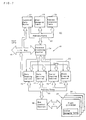
- FIG. 1 shows an example of the computer system in which the semiconductor external storage system of the present invention is incorporated;
- CPU 10 communicates via system bus 13 with main memory 15, bus control unit 16 and coprocessor 14 for arithmetic operations which is optional.
- the communications between CPU 10 and its associated peripheral devices are done via bus control unit 16.
- bus control unit 16 is connected to the peripheral devices via family bus 18.
- peripheral devices external storage system 20 made of a flash memory which is an embodiment of the present invention is connected, and communication device 21, hard file 22 and optical disk 23 are also connected to family bus 18.
- 24 is a display controller and 25 is a CRT.
- Such a computer system can be built from, for instance, an IBM PS/2 personal computer (IBM and PS/2 are trademarks of International Business Machines Corporation).
- Direct memory access control unit (DMAC) 12 is provided to enable memory accesses by all or selected peripheral devices. For this, at least part of family bus 18 is multipoint-connected to DMAC 12. Although not shown in the figure, an arbitration circuit is provided in each peripheral device to which the DMA access is allowed, and assigned an arbitration level (priority). On the DMAC 12 side, central arbitration control circuit 11 is provided which performs arbitration work between a plurality of peripheral devices demanding a DMA access at the same time and notifies DMAC 12 of which peripheral device has been allowed a DMA access. For details of the DMA control by DMAC 12 and central arbitration control circuit 11, reference is made to the US Patent No. 4,901,234.
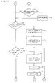
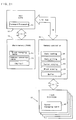
- FIG. 2 shows details of the functional structure of semiconductor external storage system 20.
- This semiconductor external storage system includes control unit 30 connected to family bus 18, and flash memory 32 connected to semiconductor memory bus 31.
- Control unit 30 includes command processing section 34, block managing table 35, address conversion table 36 and buffer 37 which are interconnected by control unit bus 33.
- Flash memory 32 consists of a plurality of memory blocks 320 (321-32i) each containing a plurality of sectors.
- memory block 320 a flash memory chip is assumed which allows only a change from 1 to 0 and is all set to 1 by block erasure, but of course it should be noted that a chip could be used which is opposite to those.
- Command processing section 34 includes an arbitration circuit and performs a DMA transfer and I/O control.
- Address conversion table 36 is to convert the logical address sent form CPU 10 through family bus 18 to the physical address of flash memory 32, and consists of a random access memory. This random access memory can include buffer 37.
- Bus control section 38 has a well-known receiver/driver used for interconnecting semiconductor memory bus 31 and control unit bus 33. Although bus control section 38 is constructed so as to accomplish parallel transfer of 16 bits between buses 31 and 33 in this embodiment, the present invention of course is not limited to such parallel transfer.
- Command processing section 34 manages data reading section 40, data writing section 41, copying section 42 and block erasing section 43.
- Flash memory 32 is managed as a collection of sectors.
- individual memory blocks 320 constituting flash memory 32 consist of 512 sectors, and each sector includes 512 bytes.
- the numbers of sectors and bytes may be changed depending on the storage capacity of memory block 320 and the architecture.
- memory block as used herein means a region on the memory chip which can be collectively erased by the block erasing section.
- one memory block corresponds to one memory chip in this embodiment, a plurality of memory blocks could exist in one memory chip, and one sector could correspond to one memory block as in the example of the sector erase type memory described later.
- FIG. 3 shows the hardware arrangement of semiconductor external storage system 20 of Figure 2.
- the respective functional portions of command processing section 34, data reading section 40, data writing section 41, copying section 42 and erasing section 43 are built with a microprocessor 50.
- the micro code controlling the microprocessor 50 is stored in ROM 52. Since block managing table 35 and address conversion table 36 are often modified and very fast access is required, they are formed on RAM 54.
- Microprocessor 50 communicates with the host CPU 10 via I/O register 56 at any time.
- Data transfer control unit 58 connects I/O bus 18 and local bus 33 as needed, thereby enabling data transfer between buffer 37 and flash memory (EEPROM) 32. Except for data transfer, these buses are disconnected and microprocessor 50 can function independently of host CPU 10.
- EEPROM flash memory
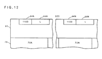
- each memory block 320 the first several sectors of each memory block 320 are used as sector managing table 60, in which the status 64 and logical address L 66 of each sector are stored.
- the remaining sectors of each memory block 320 are used as data region 70 (70A-70N).
- the size of sector managing table 60 depends on the memory block and the capacity of the sectors included therein, and in the above described example of 512 sectors per block and 512 bytes per sector, four sectors are required as the sector managing table.
- a logical address is assigned as described later.
- Sector managing table 60 includes a plurality of entries each of four bytes, and in the first entry thereof, the number of times 62 the related memory block 40 was erased is stored. In the second entry, status 64 and logical address 66 of the first sector (in this case, sector 4) used as data region 70A in the related memory block are stored. In the third entry, status 64 and logical address 66 of the next sector 70B or sector 5 are stored, and similarly, the status and logical addresses of the subsequent respective sectors are sequentially stored.
- Status 64 of a sector is indicated by a 4-bit status flag as described below. Since the status flag is on the flash memory, the bit change is limited in one direction.
- command processing section 34 communicates with CPU 10 via buffer 37. That is, the CPU command and data are DMA-transferred to buffer 37 under control of DMAC 12, and command processing section 34 fetches the command from buffer 37 and executes it. Since flash memory 32 is seen from CPU 10 as if it were a hard disk or floppy disk, the command transferred to buffer 37 is the same type as the command for such disk and contains sector address L in addition to the OP code. In external storage system 20, the sector address L is treated as logical address 66. Address conversion table 36 which provides the relationship between the sector address L (logical address 66) and physical address A (L) (pointer 68) of memory block 40 is held on RAM 54 with the construction as shown in Figure 5.
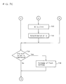
- Command processing section 34 usually independently executes processes such as sector writing and block erasing. It receives the command and data from host CPU 10 by interruption.
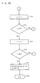
- the normal processing is outlined in Figures 7 - 8.
- the block erasing process (later described in detail) is started.
- the sector copy to other memory blocks is undertaken to save valid sectors as described later.
- the command processing section holds the number of times the memory block was erased and thereafter commands block erasing section 43 to execute block erasing of the correspond- ing memory block ie (720 - 724).
- the number of erasing times is stored and managed in the first four bytes of the sector managing table, and it is incremented by one after completion of the erasure and written back (728).
- the erased block ie is made to be blank block ib (730), the records of the sector managing table and block managing table 35 are updated. That is, the number B (i, 1) of empty sectors in the memory block i is made to be M and the number B (i, 2) of effective sectors is made to be 0 (732, 734).
- the memory block i is selected as the memory block ie which is the erase candidate used to make uniform the number of erasing times, regardless of whether the number of the "valid" sectors is large or small (736). If there is no further memory block ie to be erased in all the memory blocks and no blank sector iw exists, the request for memory replacement is displayed on CRT 25 ( Figure 1) (738, 740). This display may be done earlier so as to leave time to spare.
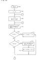
- command processing section 34 accepts a command from host CPU 10 (802), it executes the processing required for a sector reading (804, 806), a sector writing (808, 810) or sector erasing (812, 814).
- command processing section 34 looks up address conversion table 36 for the logical (sector) address 66 in the command and obtains the corresponding physical address 68.
- the physical address 68 consists of a block address (i) specifying a particular memory block 32i of flash memory 32, and a sector address (j) specifying a particular sector j in that block.
- Figure 9 shows the details of the initialization process of the block managing table and address conversion table.
- the block number i and sector number j are initialized, the number of empty sectors B (i, 1) and the number of valid sectors B (i, 2) are both set to zero (902, 904), and the status of the j-th sector in block i and data S (i, j) of pointer L are obtained from sector managing table 60 (906). If the sector is vacant, add one to the number of blank sectors B (i, 1) in block i.
- Figure 10 shows details of the file recovery. If the power supply is disconnected during a file writing by an accident or the like, the data in buffer 37 or RAM 54 is lost. Then, the old file is recovered when the power is turned on again. First, the directory information and file allocation information are read out to obtain the leading sector number K of the file (1002, 1004). As the sectors corresponding to the sector numbers written until the power was turned off, both invalid sectors having old data and valid sectors having new data exist. Then, an invalid sector having the sector number K is searched, and if there is one present, the data of the sector is moved to a new blank sector after obtaining the user's confirmation to make it valid. The existing valid sector is made invalid (1010). The user's confirmation is obtained because, if the old data comprises plural versions, confirmation is obtained as to which one should be selected. A similar processing is done for all the sectors constituting the file (1014). The old file is reconstructed by gathering the data of invalid sectors in this way.
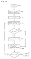
- FIG 11 is a detailed flow of the sector reading (step 806 of Figure 8), in which a physical address A (L) 68 corresponding to a given logical address L 66 is obtained from address conversion table 36, the positions sectors 70A - 70N are found, and data (AL) is set in data reading section 40 and DMA-transferred to CPU 10.
- a physical address A (L) 68 corresponding to a given logical address L 66 is obtained from address conversion table 36
- the positions sectors 70A - 70N are found
- data (AL) is set in data reading section 40 and DMA-transferred to CPU 10.
- command processing section 34 first obtains the logical address L given by host CPU 10 from buffer 37, and then looks up address conversion table 36 to obtain physical address A (L). Further, it traverses block managing table 35 to find the position of the blank sector 70N in data region 70.
- the memory block iw containing the new sector 70N may exist in the same memory block 320 as the old sector 70A or in another memory block.
- Figure 13 shows details of the above sector write processing.
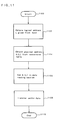
- the logical address L included in the command given from host CPU 10 is obtained (1302). And, if the processing of the later described file allocation information is required, that processing is done (1304, 1306) and then the physical address A (L) is obtained from address conversion table 36 (1308). Further, the old memory number i and sector number j are obtained for the A (L) (1314). Then, the memory address P of the blank sector in the memory block iw in which the writing is done is obtained, and this P is set in data writing section 41 and the sector data is written (1316 - 1320).
- the sector number k of the writing destination is obtained from P, the data S (iw, k) of the pointer is made valid, L is stored, and P is made to be the physical address A (L) (1322 - 1326). Then, in order to logically erase the old data at the same logical address, the value S (i, j) of the old pointer L of the memory block is made invalid (1330) and the number of valid sectors B (i, 2) is decreased by one (1332). Moreover, it is determined whether or not the block i is that to be erased next (1334), and the number of blank sectors B (iw, 1) is reduced by one (1336).
- the memory block having blank sectors is renewed as the memory block iw in which next writing is done (1340).
- the blank memory block selected as the copying memory block for saving the sector data is excluded.
- the determination of the block erasing and the processing are done (1342).
- command processing section 34 invalidates the value S (i, j) of the pointer (1508) and decrements the number of "valid" sectors B (i, 2) in the memory block i in the block managing table by one (1510). This logically erases the sector data, and physically holds it as it is valid. And, the physical address A (L) of the address conversion table is made to be zero, and the number of the remaining "valid" sectors is compared with the erase candidate memory block ie. If the number is smaller, this memory block i is selected as a candidate ie of the memory block to be erased next (1514).
- the number of "blank” sectors is always kept greater than a fixed value by the block erasing processing based on the block managing table and sector managing table.
- the "blank” sectors are used as destinations at which data is written or copied at the time of data writing or erasing. As shown in Figure 14, there are many "empty" sectors initially existing in one memory block 321, but “valid" sectors and “invalid” sectors gradually increase. And, when the number of "valid” sectors 70 remaining in the memory block 321 becomes smaller than the predetermined value, the "valid" sectors 70 are copied into “empty” sectors in another memory block 322, and then the content of the memory block 321 is erased in bulk to make them all "blank” sectors.
- the command from CPU 10 is executed by interruption even during the processing of copying sectors or erasing memory blocks. For instance, if the command of CPU 10 is for data writing, a memory block 323 other than the memory block 322 which is currently copying data is selected, and a writing process is done in parallel with the copying. Consequently, the interrupt function (parallel processing) is executed as long as blank sectors are secured, and thus the execution of the command from CPU 10 is not to wait.
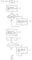
- step 1334 of Figure 13C and step 1514 of Figure 15 a processing is done to minimize the number of valid sectors of the memory block to be erased, thereby suppressing the amount of copying to a small value. For this, if a certain sector now becomes invalid, the number of valid sectors of the memory block i including that sector is compared with the number of valid sectors of the erasing candidate memory block ie to determine the next erasing candidate. The details of this are shown in Figure 16.
- the number of erasing times E (i) of a memory block i in which a sector has now become invalid is compared with the upper allowance value X of the number of erasing times of that memory.
- This upper limit value X is set to, for instance, 10,000 times or 100,000 times depending on the specification of the memory block. If X is exceeded or there are blank sectors B (i, j) in the memory block i, it is not necessary to change the erasing candidate and the determination terminates (1602, 1610).
- E (i) has not yet reached the upper limit X, then it is checked whether or not the difference between the memory block having the largest number of erasing times Q among the all memory blocks and the number of erasing times E (ie) of the erasing candidate memory block ie is equal to or smaller than the maximum allowed value R for deviation of the number of erasing times (1604).
- R an appropriate value between 100-1000 is selected for instance. If the deviation is larger than R, the examination of the memory block i is not required and the determination terminates. If, conversely, it is smaller than R, comparison of the number of valid sectors B (i, 2) is done (1606).
- the memory block i If the memory block i has only valid sectors B (i,2) less than the erasing candidate memory block ie, the memory block i is newly replaced as the next erasing candidate memory block ie (1608). Incidentally, since the total number of sectors in the memory block i is known, it will be understood that the comparison of i and ie may be done by the number of invalid sectors instead of the number of valid sectors. Referring to Figure 17, the detail of the determination processing of block erasing (step 1342 of Figure 13 C and step 1516 of Figure 15) is described.
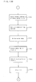
- the number of valid sectors B (ie, 2) of the erasing candidate memory block ie is compared with a predetermined value S (1702), and if the number of valid sectors becomes smaller, sector copying section 42 is instructed to copy and save the valid sectors in the block ie to the memory block ib for copying (1706).
- the next writing or copying processing is hindered if the number of the blank sectors in all the memory blocks is small though there are many valid sectors.
- the total number of blank sectors B(, 1) is smaller than a predetermined value T, sector copying processing is similarly performed for erasing (1704, 1706).
- the conventional file system only updates the file allocation information when a file is erased by CPU 10, and it does not inform the external storage of which sectors were erased.
- this problem can be solved by comparing the file allocation information as shown in Figs. 18 and 19 without rewriting the file system. That is, command processing section 34 has a function which compares the new and old file allocation information FAT. For this, the file allocation information is utilized for which CPU 10 manages the logical address L.
- Figure 20 shows a comparison of the processing times for sector writing in the conventional scheme (A) and the scheme of the present invention (B).
- A the conventional scheme
- B the scheme of the present invention
- a block is erased after all the data in the block are saved in the main memory or buffer at the beginning, and thereafter the data are written back to the memory block along with the newly updated data.
- the processing in the host CPU is interrupted during that time.
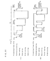
- Figure 21 shows another embodiment of the present invention, which is different in that command processing function 34 is provided by host CPU 10, as compared with the example of Figure 2. Also, block managing table 35 and address conversion table 36 are located on main memory 15 (including a buffer) and referenced by the host CPU. Host CPU 10 sends an instruction to memory controller 80 via I/O bus 18 for a sector reading or writing.
- the memory controller is formed as an integrated circuit on a silicon substrate which is separate from the host CPU, and provides the functions of data reading 40, data writing 41, sector copying 42 and block erasing in addition to buffer 37.
- Memory controller 80 can access to flash memory 32 independently of host CPU 10, and notify the host CPU of the end of a task via I/O bus 18. Since the other operations are the same as the embodiment of Figure 2, the explanation thereof is omitted.
- Figure 22 shows another embodiment of the present invention which uses a sector erase type flash memory as memory block 32.
- the sector erase type is a type in which the size of a memory block erased in bulk is equal to the physical size of the file sector. Since the erasing is performed for each sector in this example, the sector saving prior to block erasure is not necessary as compared with the example of Figure 2, and accordingly there is no sector copying section 42, and instead of block erasing section 43, sector erasing section 82 is formed on a microprocessor to perform the saving and recovery of the number of erasing times of sectors.
- sector managing table 60 is provided for each unit of memory block 320, or sector 70.
- the status and the number of erasing times of sectors are recorded in sector managing table 60, and empty sectors for writing are secured in consideration of the number of erasing times of all the sectors.
- the normal processing of the command processing section is used to check the buffer, and if there is a command, executes a sector writing or erasing as shown in Figure 7. However, as shown in Figure 23, the processing performing a sector copying prior to n sector erasing is unnecessary, and the erasing of invalid sectors is immediately executed (727-733). Further, as shown in Figure 24, processing is required to save the number of erasing times of a sector prior to the erasing of the sector and for writing it back (1705-1707).
- the semiconductor memory may be divided into a plurality of groups each having a plurality of memory blocks, and the above described managing and control of blocks and sectors may be performed for each group.
- a semiconductor external storage system using a flash memory which can process data reading and writing at high speed in response to the command of the host CPU.
- an external storage system is obtained in which, even if the command of the host CPU frequently rewrites a particular sector of the flash memory, the number of erasing times of sectors are not biased on the actual flash memory and the whole can be effectively utilized.
- a semiconductor memory is used as an external storage device consisting of a flash memory and comprised of a plurality of memory blocks each including at least one sector, and a control section performing control over said memory blocks
- a method has been described for controlling the external storage device of a computer system wherein said control section converts the logical address included in the command of said host processor to a physical address indicating the sector in a particular memory block by address conversion means, selects a memory block for data writing and a memory block for erasure to be erased next to acquire said memory block for data writing, respectively, on the basis of the record of block managing means which has sequentially recorded therein the number of times each memory block was erased and the status of each sector and memory block, writes the data to be written received from said host processor into said memory block for writing, and erases said selected memory block for erasure.
- Command processing section 34 always prepares memory blocks and sectors for writing or erasing and copying in preparation for the command processing of the host CPU, and records and holds the correspondence relation between the physical address of the selected memory block 32i or sector and the command of the host CPU in address conversion table 36.
- the status of memory blocks and sectors is recorded in respective managing tables 35 and 60, and used for control of processings such as writing, erasing and copying in preparation for or in response to the command of the host CPU.
Description
- The present invention relates to computer memory devices using electrically erasable nonvolatile memory, known as flash EEPROM or flash memory and, more particularly, to a method for controlling such a memory for use in e.g. semiconductor external storage systems which can replace the magnetic disk in a conventional computer system.
- As portable personal computers such as notebook type ones have spread, the requirement for small-sized, lightweight and low power consumption computer systems has increased. External storage using semiconductor memory has a low power consumption and can operate at a high speed because it does not use a mechanical drive system such as the magnetic disk, in addition, it consists of small memory modules, and thus it is small-sized, lightweight, and has a large degree of freedom with respect to shape as compared with the magnetic disk, and is also easily made in the form of a card.
- However, the conventional semiconductor memory has many problems with respect to such points as capacity and battery backup. If SRAM is used as the memory, the cost is high and the capacity becomes small though the backup time by a battery becomes long. For DRAM which is excellent in cost and capacity, the standby power consumption is large and the backup time is limited to one week or so. There is also a danger of data loss due to a problem in the battery system. EEPROM is costly though it requires no battery.
- A block erase type flash memory has been developed as a memory to solve these problems. Its memory element consists of one transistor as DRAM, and it can be provided with high density and it is expected to have a bit cost equivalent to or less than DRAM (low cost, large capacity) depending on the future market. The memory element is nonvolatile and requires no battery backup. The outline of such flash memory is introduced by Richard D. Pashley et al. in "Flash memories: the best of two worlds", IEEE SPECTRUM, Dec. 1989, pp. 30-33. Also, a similar flash memory is disclosed in Japanese Published Unexamined Patent Application No. 2-10598.
- However, the flash memory has limitations which SRAM and DRAM do not have. First, the erase/program cycles have an upper limit of the order of 100,000. In addition, the programming of memory bits is a one-way process and change is allowed only from 0 to 1 or 1 to 0. For change in the opposite direction, it is necessary to set the whole memory block to 0 or 1 by block erasure. Erasing usually takes several tens of milliseconds, and block erasure requires special procedures such as verify which takes a further several seconds.
- If a semiconductor memory consisting of such flash memory is connected to the bus of a host computer as an alternative to the traditional magnetic disk, a specific sector is very often written by the host computer and reaches the upper limit of the erase/program cycles considerably earlier than other sectors. Further, the sector writing takes a lot of time. The reason for this is that, to modify several bytes in the sector, all the data within the memory block including the sector are temporarily saved in the memory space of the host computer, and new data is written back to empty sectors after erasing of the memory block. It takes several seconds to write a sector in a semiconductor memory having a capacity of 1M bits or more. In addition, a special program is required to connect a semiconductor memory to the bus of the host computer.
- To solve these problems, the development of a sector erase type flash memory is needed. For instance, 27F010 from SEEQ TECHNOLOGY CORPORATION (1024K flash EPROM) allows not only the chip erasure which erases all the bits of the memory chip (change to logical one) but also the sector erasure which erases only a specific sector. In this scheme, the saving or writing back of sectors other than those to be erased can be avoided. However, it takes on the order of several tens of milliseconds because the erasing of old sectors is done along with the writing of sectors, and thus the obtained performance is equivalent to or less than the magnetic disk. In addition, the problem is not solved that a particular sector is written very often by the host computer and reaches the allowed erase/program cycles somewhat earlier than other sectors, and thus the sectors cannot effectively be used as the whole flash memory. Further, the sector erase type has a chip structure which is more complicated than the block erase type, and that there are also problems with respect to cost and erase/program cycles.
- Many of these problems are considered to be due to the control scheme in which the block and sector addresses of the external storage are controlled by the host computer, that is, the physical address of the external storage is determined by the logical address possessed by the command of the host computer.
- The objects of the invention are achieved by the apparatus as set forth in the independent claim.
- This invention provides a memory control system for controlling a flash memory, said flash memory being comprised of a plurality of blocks with each block being comprised of at least one sector, said system comprising: command processing means for receiving a write command from an external central processing unit and controlling said memory control system to execute said write command to write data into said flash memory; sector management means for, under control of said command processing means, keeping track of information concerning the contents of each sector, such information including whether a sector contains valid data, invalid data or no data; and address conversion means for, under control of said command processing means, keeping track of which logical sector addresses, addresses used by said central processing unit, correspond to which physical sector addresses of said flash memory; wherein said command processing means includes: means for re-directing said write instruction to a physical sector address of said flash memory which said sector management means indicates as containing no data; and means for updating said address conversion means based on the redirection of said data.
- Advantageous features of embodiments of the invention are set out in the attached dependent claims. The present invention enables the provision of an external storage system using a semiconductor memory which can process the data reading and writing between the host computer at a speed higher than the conventional magnetic disk. The whole semiconductor memory is effectively used for a long period of time without frequently writing and erasing only a particular sector in the semiconductor memory. The semiconductor external storage system is compatible with a conventional magnetic disk when it is connected to a computer system. Files can easily be restored even if the power is disconnected in a writing.
- This is achieved by providing flexibility in the address relation between the host computer and the external storage, and by introducing an address control scheme in which the physical address of the external storage is not one-sidedly decided on by the logical address possessed by the command of the host computer. On the external storage side, a memory block or sector for writing or copying is always prepared for the command processing of the host, and the correspondence relationship of the physical address of the selected memory block or sector with the command of the host computer is recorded and held in an address conversion table. The status of the memory block and sector is recorded and managed in the respective managing tables.
- On the external storage side, an optimum memory block or sector can be selected in consideration of the processing speed of the host computer and the utilization efficiency of the semiconductor memory. In addition, the processing speed of the host computer can be increased without waiting for the command of the host, or executing the command processing in parallel with the command of the host. That is, memory blocks in which data can be written or erased are prepared beforehand on the basis of the record in the memory managing means, thereby occasioning a fast processing in response to the command of the host processor. Moreover, since the memory blocks and sectors of the semiconductor memory can be totally managed and the physical address can freely he selected in consideration of the utilization efficiency, the unnecessary frequent erasure of a particular memory block in the semiconductor memory is eliminated and the whole memory is effectively used over a long period of time. Since the host computer can give a command to the external storage without considering the physical address and receive the result of the process, compatibility with the traditional magnetic disk can he maintained. Also, no rewriting of data directly connected with the command address of the host processor is performed, and thus files can easily be recovered.
- Embodiments of the invention will now be described, by way of example only, with reference to the accompanying drawing, wherein:
- Figure 1 shows an example of the computer system in which the semiconductor external storage system of the present invention is incorporated;
- Figure 2 shows the detail of the functions of an embodiment of the semiconductor external storage system of the present invention;
- Figure 3 shows the details of the construction used for implementing the functions of the semiconductor external storage system of Figure 2;
- Figure 4 shows an example of the sector construction of a memory block;
- Figure 5 shows an example of the construction of the address conversion table;
- Figure 6 shows showing an example of the construction of the block managing table;
- Figure 7A is a flowchart showing the normal processing of the command processing section;
- Figure 7B is a flowchart showing the normal processing of the command processing section;
- Figure 7C is a flowchart showing the normal processing of the command processing section;
- Figure 8 is a flowchart showing the interruption processing of the command processing section;
- Figure 9A is a flowchart showing the process of initializing the managing table and conversion table in Figure 7A;
- Figure 9B is a flowchart showing the process of initializing the managing table and conversion table in Figure 7A;
- Figure 10 is a flowchart showing the detail of the file recovery processing in Figure 7A;
- Figure 11 is a flowchart showing the detail of the sector read processing in Figure 8;
- Figure 12 is a representation explaining the sector write processing;
- Figure 13A is a flowchart showing the detail of the sector write processing in Figure 7A;
- Figure 13B is a flowchart showing the detail of the sector write processing in Figure 7A;
- Figure 13C is a flowchart showing the detail of the sector write processing in Figure 7A;
- Figure 14 is a representation explaining the sector erase processing in Figure 7A;
- Figure 15 is a flowchart showing the detail of the sector erase processing in Figure 7A;
- Figure 16 is a flowchart showing the detail of the compare processing of i and ie in Figure 15;
- Figure 17 is a flow chart showing the detail of the block erase determination and start in Figure 15;
- Figure 18 shows an explanatory view of an example of sector erasing by comparison of the file location information;
- Figure 19 is a flowchart showing the details of the sector erasing of Figure 18;
- Figure 20 is a time chart diagram showing the relationship between the normal processing of the command processing section in Figure 2 and the interruption processing of CPU;
- Figure 21 shows an example of the computer system in which the semiconductor external storage system according to another embodiment of the present invention is incorporated;
- Figure 22 shows an example of the computer system in which the external storage system according to still another embodiment of the present invention is shown;
- Figure 23 is a flowchart showing part of the normal processing of the command processing section in Figure 22;
- Figure 24 is a flowchart showing the processings of the sector erase determination and start in Figure 22;
- Figure 25 is a time chart diagram showing the relationship between the normal processing of the command processing section and the interruption processing of the CPU in Figure 22.
- Figure 1 shows an example of the computer system in which the semiconductor external storage system of the present invention is incorporated;
CPU 10 communicates viasystem bus 13 withmain memory 15, bus control unit 16 andcoprocessor 14 for arithmetic operations which is optional. The communications betweenCPU 10 and its associated peripheral devices are done via bus control unit 16. For this, bus control unit 16 is connected to the peripheral devices viafamily bus 18. As the peripheral devices,external storage system 20 made of a flash memory which is an embodiment of the present invention is connected, andcommunication device 21,hard file 22 andoptical disk 23 are also connected tofamily bus 18. 24 is a display controller and 25 is a CRT. Of course other peripheral devices can be connected. Such a computer system can be built from, for instance, an IBM PS/2 personal computer (IBM and PS/2 are trademarks of International Business Machines Corporation). - Direct memory access control unit (DMAC) 12 is provided to enable memory accesses by all or selected peripheral devices. For this, at least part of
family bus 18 is multipoint-connected toDMAC 12. Although not shown in the figure, an arbitration circuit is provided in each peripheral device to which the DMA access is allowed, and assigned an arbitration level (priority). On theDMAC 12 side, centralarbitration control circuit 11 is provided which performs arbitration work between a plurality of peripheral devices demanding a DMA access at the same time and notifiesDMAC 12 of which peripheral device has been allowed a DMA access. For details of the DMA control byDMAC 12 and centralarbitration control circuit 11, reference is made to the US Patent No. 4,901,234. - Figure 2 shows details of the functional structure of semiconductor
external storage system 20. This semiconductor external storage system includescontrol unit 30 connected tofamily bus 18, andflash memory 32 connected tosemiconductor memory bus 31.Control unit 30 includescommand processing section 34, block managing table 35, address conversion table 36 andbuffer 37 which are interconnected bycontrol unit bus 33.Flash memory 32 consists of a plurality of memory blocks 320 (321-32i) each containing a plurality of sectors. In this embodiment, asmemory block 320, a flash memory chip is assumed which allows only a change from 1 to 0 and is all set to 1 by block erasure, but of course it should be noted that a chip could be used which is opposite to those.Command processing section 34 includes an arbitration circuit and performs a DMA transfer and I/O control. Address conversion table 36 is to convert the logical address sentform CPU 10 throughfamily bus 18 to the physical address offlash memory 32, and consists of a random access memory. This random access memory can includebuffer 37. -
Bus control section 38 has a well-known receiver/driver used for interconnectingsemiconductor memory bus 31 andcontrol unit bus 33. Althoughbus control section 38 is constructed so as to accomplish parallel transfer of 16 bits betweenbuses Command processing section 34 managesdata reading section 40,data writing section 41, copyingsection 42 andblock erasing section 43. -
Flash memory 32 is managed as a collection of sectors. In this embodiment, individual memory blocks 320 constitutingflash memory 32 consist of 512 sectors, and each sector includes 512 bytes. The numbers of sectors and bytes may be changed depending on the storage capacity ofmemory block 320 and the architecture. - It should be noted that the term memory block as used herein means a region on the memory chip which can be collectively erased by the block erasing section. Although one memory block corresponds to one memory chip in this embodiment, a plurality of memory blocks could exist in one memory chip, and one sector could correspond to one memory block as in the example of the sector erase type memory described later.
- Figure 3 shows the hardware arrangement of semiconductor
external storage system 20 of Figure 2. In the figure, the respective functional portions ofcommand processing section 34,data reading section 40,data writing section 41, copyingsection 42 and erasingsection 43 are built with amicroprocessor 50. The micro code controlling themicroprocessor 50 is stored inROM 52. Since block managing table 35 and address conversion table 36 are often modified and very fast access is required, they are formed onRAM 54.Microprocessor 50 communicates with thehost CPU 10 via I/O register 56 at any time. Datatransfer control unit 58 connects I/O bus 18 andlocal bus 33 as needed, thereby enabling data transfer betweenbuffer 37 and flash memory (EEPROM) 32. Except for data transfer, these buses are disconnected andmicroprocessor 50 can function independently ofhost CPU 10. - As shown in Figure 4, the first several sectors of each
memory block 320 are used as sector managing table 60, in which thestatus 64 andlogical address L 66 of each sector are stored. The remaining sectors of eachmemory block 320 are used as data region 70 (70A-70N). The size of sector managing table 60 depends on the memory block and the capacity of the sectors included therein, and in the above described example of 512 sectors per block and 512 bytes per sector, four sectors are required as the sector managing table. To eachsector 70A-70N, a logical address is assigned as described later. These sectors including sector managing table 60 are formatted on a memory chip using a format program. - Sector managing table 60 includes a plurality of entries each of four bytes, and in the first entry thereof, the number of
times 62 therelated memory block 40 was erased is stored. In the second entry,status 64 andlogical address 66 of the first sector (in this case, sector 4) used asdata region 70A in the related memory block are stored. In the third entry,status 64 andlogical address 66 of thenext sector 70B orsector 5 are stored, and similarly, the status and logical addresses of the subsequent respective sectors are sequentially stored. -
Status 64 of a sector is indicated by a 4-bit status flag as described below. Since the status flag is on the flash memory, the bit change is limited in one direction. - 1111 = blank
- 1110 = valid
- 1100 = invalid
- 0000 = under erasure
- Returning to Figures 2 and 3,
command processing section 34 communicates withCPU 10 viabuffer 37. That is, the CPU command and data are DMA-transferred to buffer 37 under control ofDMAC 12, andcommand processing section 34 fetches the command frombuffer 37 and executes it. Sinceflash memory 32 is seen fromCPU 10 as if it were a hard disk or floppy disk, the command transferred to buffer 37 is the same type as the command for such disk and contains sector address L in addition to the OP code. Inexternal storage system 20, the sector address L is treated aslogical address 66. Address conversion table 36 which provides the relationship between the sector address L (logical address 66) and physical address A (L) (pointer 68) ofmemory block 40 is held onRAM 54 with the construction as shown in Figure 5. - Now, the operation of
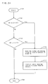
control unit 30 ofexternal storage system 20 will be described.Command processing section 34 usually independently executes processes such as sector writing and block erasing. It receives the command and data fromhost CPU 10 by interruption. The normal processing is outlined in Figures 7 - 8. - First, in the first step of Figure 7 (Figure 7A - 7C), the initialization of the block managing table and address conversion table is done (702). Then, it is determined whether or not file recovery is required for disconnection of the power supply or the like, and the process therefore is executed if necessary (704, 706). Next, it is checked whether there is any command sent from
host CPU 10 to buffer 37 (708). If there is a write command, the existence of blank sectors inmemory block 40 is checked (total number B (, 1) > 0), and a writing is performed if there is a blank sector (710 - 714). If it is a sector erase command, the erasing process of the corresponding sector is done (716, 718). If a certain memory block is determined to be a memory block ie to be erased, the block erasing process (later described in detail) is started. In the block erasing process, the sector copy to other memory blocks is undertaken to save valid sectors as described later. When the sector copy is terminated, the command processing section holds the number of times the memory block was erased and thereafter commandsblock erasing section 43 to execute block erasing of the correspond- ing memory block ie (720 - 724). The number of erasing times is stored and managed in the first four bytes of the sector managing table, and it is incremented by one after completion of the erasure and written back (728). Then, the erased block ie is made to be blank block ib (730), the records of the sector managing table and block managing table 35 are updated. That is, the number B (i, 1) of empty sectors in the memory block i is made to be M and the number B (i, 2) of effective sectors is made to be 0 (732, 734). - However, if the number of erasing times of a certain memory block i to be collectively erased is smaller than that of a memory block ie, an erase candidate, by a certain value, the memory block i is selected as the memory block ie which is the erase candidate used to make uniform the number of erasing times, regardless of whether the number of the "valid" sectors is large or small (736). If there is no further memory block ie to be erased in all the memory blocks and no blank sector iw exists, the request for memory replacement is displayed on CRT 25 (Figure 1) (738, 740). This display may be done earlier so as to leave time to spare.
- The request for processing from
host CPU 10 toexternal storage system 20 is accepted by the previously mentioned interruption in the normal processing. As shown in Figure 8, whencommand processing section 34 accepts a command from host CPU 10 (802), it executes the processing required for a sector reading (804, 806), a sector writing (808, 810) or sector erasing (812, 814). To execute each command,command processing section 34 looks up address conversion table 36 for the logical (sector) address 66 in the command and obtains the correspondingphysical address 68. Thephysical address 68 consists of a block address (i) specifying a particular memory block 32i offlash memory 32, and a sector address (j) specifying a particular sector j in that block. - The details of each processing of the
command processing section 34 will now be described. First, the initialization of the block managing table and address conversion table (Figure 7A, step 702) is described. Figure 9 (Figures 9A, 9B) shows the details of the initialization process of the block managing table and address conversion table. The block number i and sector number j are initialized, the number of empty sectors B (i, 1) and the number of valid sectors B (i, 2) are both set to zero (902, 904), and the status of the j-th sector in block i and data S (i, j) of pointer L are obtained from sector managing table 60 (906). If the sector is vacant, add one to the number of blank sectors B (i, 1) in block i. If the sector is not vacant, then the sector is checked for validity, and if it is valid,physical address 68 is stored in L-th A (L) of address conversion table 36 (914) and one is added to the number of valid sectors B (i, 2) (916). A similar processing is executed until sector number j reaches the total number of sectors M in block i (920). Further, a similar processing is repeated for all blocks N (922 - 924). The number iw of the block in which a sector writing is performed, the number ie of the candidate block for erasure, and the number ib of the blank block in which data is to be saved for the erasure are determined (926). - The file recovery (Figure 7A, step 706) is described below. In the conventional magnetic disk file, data is overwritten on the sector when the sector is rewritten, and thus, if a power failure occurs in the course of rewriting a file for instance, both old and new files would be lost. On the other hand, in the present invention, a new sector is found for the sector rewriting without overwriting the old sector, and thus the old data continues to be valid until the block including the data is erased (however, the status flag of the sector has already been rewritten to invalid). Accordingly, if a file writing has failed, it is possible in most cases to find
old sector 66 from the value of L in S (i, j) and reproduce the file regardless ofstatus flag 64. - Figure 10 shows details of the file recovery. If the power supply is disconnected during a file writing by an accident or the like, the data in
buffer 37 orRAM 54 is lost. Then, the old file is recovered when the power is turned on again. First, the directory information and file allocation information are read out to obtain the leading sector number K of the file (1002, 1004). As the sectors corresponding to the sector numbers written until the power was turned off, both invalid sectors having old data and valid sectors having new data exist. Then, an invalid sector having the sector number K is searched, and if there is one present, the data of the sector is moved to a new blank sector after obtaining the user's confirmation to make it valid. The existing valid sector is made invalid (1010). The user's confirmation is obtained because, if the old data comprises plural versions, confirmation is obtained as to which one should be selected. A similar processing is done for all the sectors constituting the file (1014). The old file is reconstructed by gathering the data of invalid sectors in this way. - Figure 11 is a detailed flow of the sector reading (step 806 of Figure 8), in which a physical address A (L) 68 corresponding to a given
logical address L 66 is obtained from address conversion table 36, thepositions sectors 70A - 70N are found, and data (AL) is set indata reading section 40 and DMA-transferred toCPU 10. - Now, the sector write processing (step 714 of Figure 7A) is described. In Figures 2 and 12,
command processing section 34 first obtains the logical address L given byhost CPU 10 frombuffer 37, and then looks up address conversion table 36 to obtain physical address A (L). Further, it traverses block managing table 35 to find the position of theblank sector 70N indata region 70. And, it reads out the data received fromhost CPU 10 frombuffer 37, writes this new data into theblank sector 70N, and rewrites itsstatus flag 64N from "blank" to "valid" and thestatus flag 64A of theold sector 70A from "valid" to "invalid." Then, it stores the correspondence between thelogical address 66 and the physical address of thenew sector 70N specified byhost CPU 10 in address conversion table 36, and the record of the block managing table is renewed as to the number of blank sectors (i, 1), the number of valid sectors (i, 2) and the total number of empty sectors B (, 1). Incidentally, the memory block iw containing thenew sector 70N may exist in thesame memory block 320 as theold sector 70A or in another memory block. - Figure 13 (13A - 13C) shows details of the above sector write processing.
- First, the logical address L included in the command given from
host CPU 10 is obtained (1302). And, if the processing of the later described file allocation information is required, that processing is done (1304, 1306) and then the physical address A (L) is obtained from address conversion table 36 (1308). Further, the old memory number i and sector number j are obtained for the A (L) (1314). Then, the memory address P of the blank sector in the memory block iw in which the writing is done is obtained, and this P is set indata writing section 41 and the sector data is written (1316 - 1320). In addition, the sector number k of the writing destination is obtained from P, the data S (iw, k) of the pointer is made valid, L is stored, and P is made to be the physical address A (L) (1322 - 1326). Then, in order to logically erase the old data at the same logical address, the value S (i, j) of the old pointer L of the memory block is made invalid (1330) and the number of valid sectors B (i, 2) is decreased by one (1332). Moreover, it is determined whether or not the block i is that to be erased next (1334), and the number of blank sectors B (iw, 1) is reduced by one (1336). And, if the number of blank sectors becomes 0, the memory block having blank sectors is renewed as the memory block iw in which next writing is done (1340). However, the blank memory block selected as the copying memory block for saving the sector data is excluded. Finally, the determination of the block erasing and the processing are done (1342). - The procedure of sector erasing (step 718 of Figure 7B) is now described in detail according to Figures 14 - 15.
- In Figure 15, each time the status flag of the sectors of a certain memory block i changes from "valid" to "invalid",
command processing section 34 invalidates the value S (i, j) of the pointer (1508) and decrements the number of "valid" sectors B (i, 2) in the memory block i in the block managing table by one (1510). This logically erases the sector data, and physically holds it as it is valid. And, the physical address A (L) of the address conversion table is made to be zero, and the number of the remaining "valid" sectors is compared with the erase candidate memory block ie. If the number is smaller, this memory block i is selected as a candidate ie of the memory block to be erased next (1514). - In this embodiment, the number of "blank" sectors is always kept greater than a fixed value by the block erasing processing based on the block managing table and sector managing table. The "blank" sectors are used as destinations at which data is written or copied at the time of data writing or erasing. As shown in Figure 14, there are many "empty" sectors initially existing in one
memory block 321, but "valid" sectors and "invalid" sectors gradually increase. And, when the number of "valid"sectors 70 remaining in thememory block 321 becomes smaller than the predetermined value, the "valid"sectors 70 are copied into "empty" sectors in anothermemory block 322, and then the content of thememory block 321 is erased in bulk to make them all "blank" sectors. - The command from
CPU 10 is executed by interruption even during the processing of copying sectors or erasing memory blocks. For instance, if the command ofCPU 10 is for data writing, amemory block 323 other than thememory block 322 which is currently copying data is selected, and a writing process is done in parallel with the copying. Consequently, the interrupt function (parallel processing) is executed as long as blank sectors are secured, and thus the execution of the command fromCPU 10 is not to wait. - Incidentally, since it takes time to copy the data of valid sectors prior to block erasure, the number of copying times is preferably as small as possible. Accordingly, in step 1334 of Figure 13C and step 1514 of Figure 15, a processing is done to minimize the number of valid sectors of the memory block to be erased, thereby suppressing the amount of copying to a small value. For this, if a certain sector now becomes invalid, the number of valid sectors of the memory block i including that sector is compared with the number of valid sectors of the erasing candidate memory block ie to determine the next erasing candidate. The details of this are shown in Figure 16. First, the number of erasing times E (i) of a memory block i in which a sector has now become invalid is compared with the upper allowance value X of the number of erasing times of that memory. This upper limit value X is set to, for instance, 10,000 times or 100,000 times depending on the specification of the memory block. If X is exceeded or there are blank sectors B (i, j) in the memory block i, it is not necessary to change the erasing candidate and the determination terminates (1602, 1610). If E (i) has not yet reached the upper limit X, then it is checked whether or not the difference between the memory block having the largest number of erasing times Q among the all memory blocks and the number of erasing times E (ie) of the erasing candidate memory block ie is equal to or smaller than the maximum allowed value R for deviation of the number of erasing times (1604). R, an appropriate value between 100-1000 is selected for instance. If the deviation is larger than R, the examination of the memory block i is not required and the determination terminates. If, conversely, it is smaller than R, comparison of the number of valid sectors B (i, 2) is done (1606). If the memory block i has only valid sectors B (i,2) less than the erasing candidate memory block ie, the memory block i is newly replaced as the next erasing candidate memory block ie (1608). Incidentally, since the total number of sectors in the memory block i is known, it will be understood that the comparison of i and ie may be done by the number of invalid sectors instead of the number of valid sectors. Referring to Figure 17, the detail of the determination processing of block erasing (
step 1342 of Figure 13 C and step 1516 of Figure 15) is described. First, the number of valid sectors B (ie, 2) of the erasing candidate memory block ie is compared with a predetermined value S (1702), and if the number of valid sectors becomes smaller,sector copying section 42 is instructed to copy and save the valid sectors in the block ie to the memory block ib for copying (1706). The next writing or copying processing is hindered if the number of the blank sectors in all the memory blocks is small though there are many valid sectors. Thus, if the total number of blank sectors B(, 1) is smaller than a predetermined value T, sector copying processing is similarly performed for erasing (1704, 1706). - To efficiently reproduce blank sectors, it is needed to know the sectors erased by the host CPU as early as possible. However, the conventional file system only updates the file allocation information when a file is erased by
CPU 10, and it does not inform the external storage of which sectors were erased. In accordance with the embodiment of the present invention, when the file system was rewritten (step 1304 of Figure 13A), this problem can be solved by comparing the file allocation information as shown in Figs. 18 and 19 without rewriting the file system. That is,command processing section 34 has a function which compares the new and old file allocation information FAT. For this, the file allocation information is utilized for whichCPU 10 manages the logical address L. When the file system is rewritten byCPU 10, that information is stored at a specific logical address L by the operating system OS. Then, the old file allocation information FATO on the external storage side is read out (1902) and compared with each entry U of the new file allocation information FATN at theCPU 10 side (1908), and if there is asector 70N which was newly freed, sector erasing processing of thesector 70N is done (1912). A similar processing is performed for all entries to update the sector status on the external storage side. - In accordance with the above described embodiment of the present invention, all the sectors are substantially uniformly used and a high-speed sector writing is enabled. Figure 20 shows a comparison of the processing times for sector writing in the conventional scheme (A) and the scheme of the present invention (B). In the conventional scheme, a block is erased after all the data in the block are saved in the main memory or buffer at the beginning, and thereafter the data are written back to the memory block along with the newly updated data. Usually there are about 64-256 sectors in a block, and it takes a considerable amount of time to read out and write back all of them. The processing in the host CPU is interrupted during that time. On the other hand, in the scheme of the present invention (B), as the processing by
CPU 10 for sector writing, it is only needed to write one sector, which eliminates the need for the data saving processing that has conventionally been required, and the block erasing is independently executed incommand processing section 34 in parallel with the (other) processing ofCPU 10. Accordingly, a fairly high speed sector writing as compared with the conventional scheme, in other words, the shortening of the binding time ofCPU 10 is allowed. The reason for this is that the present invention manages memory blocks and sectors so as to always separately prepare a memory block in which sectors are written a memory block to be erased and a blank memory block. This allows the parallel execution of a sector writing and a memory block erasing, and a sector writing and a memory block erasing. - Figure 21 shows another embodiment of the present invention, which is different in that
command processing function 34 is provided byhost CPU 10, as compared with the example of Figure 2. Also, block managing table 35 and address conversion table 36 are located on main memory 15 (including a buffer) and referenced by the host CPU.Host CPU 10 sends an instruction tomemory controller 80 via I/O bus 18 for a sector reading or writing. The memory controller is formed as an integrated circuit on a silicon substrate which is separate from the host CPU, and provides the functions of data reading 40, data writing 41,sector copying 42 and block erasing in addition tobuffer 37.Memory controller 80 can access toflash memory 32 independently ofhost CPU 10, and notify the host CPU of the end of a task via I/O bus 18. Since the other operations are the same as the embodiment of Figure 2, the explanation thereof is omitted. - Further, Figure 22 shows another embodiment of the present invention which uses a sector erase type flash memory as
memory block 32. The sector erase type is a type in which the size of a memory block erased in bulk is equal to the physical size of the file sector. Since the erasing is performed for each sector in this example, the sector saving prior to block erasure is not necessary as compared with the example of Figure 2, and accordingly there is nosector copying section 42, and instead ofblock erasing section 43,sector erasing section 82 is formed on a microprocessor to perform the saving and recovery of the number of erasing times of sectors. In addition, sector managing table 60 is provided for each unit ofmemory block 320, orsector 70. The status and the number of erasing times of sectors are recorded in sector managing table 60, and empty sectors for writing are secured in consideration of the number of erasing times of all the sectors. The normal processing of the command processing section is used to check the buffer, and if there is a command, executes a sector writing or erasing as shown in Figure 7. However, as shown in Figure 23, the processing performing a sector copying prior to n sector erasing is unnecessary, and the erasing of invalid sectors is immediately executed (727-733). Further, as shown in Figure 24, processing is required to save the number of erasing times of a sector prior to the erasing of the sector and for writing it back (1705-1707). - Also in this embodiment, as shown in Figure 25, all sectors are almost evenly used and high-speed sector writing is enabled. In this example, since the erasing is done on a sector basis, the saving of data and the copying of sectors are not necessary. In the conventional scheme (A), the host CPU also needs to do the erasing of a sector each time the sector is written. In the scheme of the present invention (B), the processing of the host CPU is only used to write a sector and the other processings, for instance, sector erasing is independently processed by the memory controller, and thus the processing time of the host CPU may be short and a high-spreed sector writing is made possible.
- Incidentally, if the semiconductor has a large capacity, the semiconductor memory may be divided into a plurality of groups each having a plurality of memory blocks, and the above described managing and control of blocks and sectors may be performed for each group.
- In accordance with the present invention, a semiconductor external storage system using a flash memory is used which can process data reading and writing at high speed in response to the command of the host CPU. In addition, an external storage system is obtained in which, even if the command of the host CPU frequently rewrites a particular sector of the flash memory, the number of erasing times of sectors are not biased on the actual flash memory and the whole can be effectively utilized.
- In a computer system comprising a host processor, a semiconductor memory is used as an external storage device consisting of a flash memory and comprised of a plurality of memory blocks each including at least one sector, and a control section performing control over said memory blocks, a method has been described for controlling the external storage device of a computer system wherein said control section converts the logical address included in the command of said host processor to a physical address indicating the sector in a particular memory block by address conversion means, selects a memory block for data writing and a memory block for erasure to be erased next to acquire said memory block for data writing, respectively, on the basis of the record of block managing means which has sequentially recorded therein the number of times each memory block was erased and the status of each sector and memory block, writes the data to be written received from said host processor into said memory block for writing, and erases said selected memory block for erasure.
- To provide an external storage system using a semiconductor memory in which the data reading and writing between the host CPU can be processed faster than the conventional magnetic disk, and only a particular sector is not frequently written and erased so that the whole memory is effectively used over a long period of time. An address control scheme was introduced in which flexibility is given to the address relation between the host CPU and the external storage and the physical address of the semiconductor memory is not one-sidedly determined by the logical address possessed by the command of the host CPU.
Command processing section 34 always prepares memory blocks and sectors for writing or erasing and copying in preparation for the command processing of the host CPU, and records and holds the correspondence relation between the physical address of the selected memory block 32i or sector and the command of the host CPU in address conversion table 36. The status of memory blocks and sectors is recorded in respective managing tables 35 and 60, and used for control of processings such as writing, erasing and copying in preparation for or in response to the command of the host CPU.
Claims (4)
- A memory control system (30, 60) for controlling a flash memory (32), said flash memory being comprised of a plurality of blocks with each block being comprised of at least one sector, said system comprising:command processing means (34) for receiving a write command from an external central processing unit and controlling said memory control system to execute said write command to write data into said flash memory;sector management means (60) for, under control of said command processing means (34), keeping track of information concerning the contents of each sector, such information including whether a sector contains valid data, or no data; andaddress conversion means (36) for, under control of said command processing means (34), keeping track of which logical sector addresses, addresses used by said central processing unit, correspond to which physical sector addresses of said flash memory;wherein said command processing means (34) includes:means for re-directing said write instruction to a physical sector address of said flash memory which said sector management means indicates as containing no data; andmeans for selecting an erase candidate block wherein a block which has been previously erased a least number of times is selected;means for performing bulk erasing of said erase candidate block if the number of valid sectors in said block becomes smaller than a threshold value in order to create more sectors containing no data for use in future write operations; andmeans for updating said sector management means (60) and said address conversion means (36) in response to re-direction of said data and/or said bulk-erasing.
- The system of claim 2 wherein said bulk erasing is performed by said command processing means (34) in parallel with said re-directing of said write instruction by said means for re-directing.
- The system of claim 1 or 3 wherein said sector management means also keeps track of the number of times (62) a block has been bulk-erased, and said command processing means (34) checks said number of times (62) to determine which block should be bulk-erased next.
- The system of claims 1, 3 or 4 further comprising:block management means (35) for, under control of said command processing means (34), summarizing said information stored in said sector management means (60) on a block-by-block basis, including keeping track of, for each block, how many (74) sectors contain valid data and how many (72) sectors contain no data; andwherein said command processing means (34), using said block management means (35) checks the number (74), in said block management means (35), of sectors containing valid data and designates a block candidate for bulk-erasure based on which block has the least number of valid data sectors.
Applications Claiming Priority (2)
| Application Number | Priority Date | Filing Date | Title |
|---|---|---|---|
| JP19731891A JP2582487B2 (en) | 1991-07-12 | 1991-07-12 | External storage system using semiconductor memory and control method thereof |
| JP197318/91 | 1991-07-12 |
Publications (3)
| Publication Number | Publication Date |
|---|---|
| EP0522780A2 EP0522780A2 (en) | 1993-01-13 |
| EP0522780A3 EP0522780A3 (en) | 1993-07-28 |
| EP0522780B1 true EP0522780B1 (en) | 1997-11-26 |
Family
ID=16372465
Family Applications (1)
| Application Number | Title | Priority Date | Filing Date |
|---|---|---|---|
| EP92306064A Expired - Lifetime EP0522780B1 (en) | 1991-07-12 | 1992-07-01 | Control method for a computer memory device |
Country Status (4)
| Country | Link |
|---|---|
| US (1) | US5524230A (en) |
| EP (1) | EP0522780B1 (en) |
| JP (1) | JP2582487B2 (en) |
| DE (1) | DE69223287T2 (en) |
Cited By (16)
| Publication number | Priority date | Publication date | Assignee | Title |
|---|---|---|---|---|
| US6397314B1 (en) | 1995-07-31 | 2002-05-28 | Lexar Media, Inc. | Increasing the memory performance of flash memory devices by writing sectors simultaneously to multiple flash memory devices |
| US7681057B2 (en) | 2001-09-28 | 2010-03-16 | Lexar Media, Inc. | Power management of non-volatile memory systems |
| US7725628B1 (en) | 2004-04-20 | 2010-05-25 | Lexar Media, Inc. | Direct secondary device interface by a host |
| US7734862B2 (en) | 2000-07-21 | 2010-06-08 | Lexar Media, Inc. | Block management for mass storage |
| US7743290B2 (en) | 2004-08-27 | 2010-06-22 | Lexar Media, Inc. | Status of overall health of nonvolatile memory |
| US7774576B2 (en) | 1995-07-31 | 2010-08-10 | Lexar Media, Inc. | Direct logical block addressing flash memory mass storage architecture |
| US7865659B2 (en) | 2004-04-30 | 2011-01-04 | Micron Technology, Inc. | Removable storage device |
| US7908426B2 (en) | 1995-07-31 | 2011-03-15 | Lexar Media, Inc. | Moving sectors within a block of information in a flash memory mass storage architecture |
| US7917709B2 (en) | 2001-09-28 | 2011-03-29 | Lexar Media, Inc. | Memory system for data storage and retrieval |
| US7944762B2 (en) | 2001-09-28 | 2011-05-17 | Micron Technology, Inc. | Non-volatile memory control |
| US7949822B2 (en) | 2004-08-27 | 2011-05-24 | Micron Technology, Inc. | Storage capacity status |
| US8031536B2 (en) | 1991-11-26 | 2011-10-04 | S4, Inc. | Storage device employing a flash memory |
| US8078797B2 (en) | 1995-07-31 | 2011-12-13 | Micron Technology, Inc. | Increasing the memory performance of flash memory devices by writing sectors simultaneously to multiple flash memory devices |
| US8166488B2 (en) | 2002-02-22 | 2012-04-24 | Micron Technology, Inc. | Methods of directly accessing a mass storage data device |
| US8171203B2 (en) | 1995-07-31 | 2012-05-01 | Micron Technology, Inc. | Faster write operations to nonvolatile memory using FSInfo sector manipulation |
| US8386695B2 (en) | 2001-09-28 | 2013-02-26 | Micron Technology, Inc. | Methods and apparatus for writing data to non-volatile memory |
Families Citing this family (191)
| Publication number | Priority date | Publication date | Assignee | Title |
|---|---|---|---|---|
| US7190617B1 (en) | 1989-04-13 | 2007-03-13 | Sandisk Corporation | Flash EEprom system |
| US6230233B1 (en) | 1991-09-13 | 2001-05-08 | Sandisk Corporation | Wear leveling techniques for flash EEPROM systems |
| TW261687B (en) * | 1991-11-26 | 1995-11-01 | Hitachi Seisakusyo Kk | |
| JP3587204B2 (en) * | 1991-11-28 | 2004-11-10 | 株式会社日立製作所 | Storage device |
| JP4086083B2 (en) * | 1991-11-28 | 2008-05-14 | 株式会社日立製作所 | Information equipment with flash memory |
| JP3407317B2 (en) * | 1991-11-28 | 2003-05-19 | 株式会社日立製作所 | Storage device using flash memory |
| JPH05151097A (en) * | 1991-11-28 | 1993-06-18 | Fujitsu Ltd | Data control system for rewriting frequency limited type memory |
| US6256642B1 (en) * | 1992-01-29 | 2001-07-03 | Microsoft Corporation | Method and system for file system management using a flash-erasable, programmable, read-only memory |
| JPH05233426A (en) * | 1992-02-20 | 1993-09-10 | Fujitsu Ltd | Flash memory using method |
| JP3485938B2 (en) * | 1992-03-31 | 2004-01-13 | 株式会社東芝 | Nonvolatile semiconductor memory device |
| JP3390482B2 (en) * | 1992-06-12 | 2003-03-24 | 株式会社リコー | Facsimile machine |
| US6549974B2 (en) | 1992-06-22 | 2003-04-15 | Hitachi, Ltd. | Semiconductor storage apparatus including a controller for sending first and second write commands to different nonvolatile memories in a parallel or time overlapped manner |
| JP3328604B2 (en) * | 1992-06-22 | 2002-09-30 | 株式会社日立製作所 | Semiconductor storage device |
| JP3328605B2 (en) * | 1992-06-22 | 2002-09-30 | 株式会社日立製作所 | Semiconductor storage device |
| JP3328321B2 (en) * | 1992-06-22 | 2002-09-24 | 株式会社日立製作所 | Semiconductor storage device |
| US5740395A (en) * | 1992-10-30 | 1998-04-14 | Intel Corporation | Method and apparatus for cleaning up a solid state memory disk storing floating sector data |
| US5822781A (en) * | 1992-10-30 | 1998-10-13 | Intel Corporation | Sector-based storage device emulator having variable-sized sector |
| JP3641280B2 (en) * | 1992-10-30 | 2005-04-20 | インテル・コーポレーション | Method for determining blocks to be cleaned up in a flash EEPROM array |
| US5835933A (en) * | 1993-02-19 | 1998-11-10 | Intel Corporation | Method and apparatus for updating flash memory resident firmware through a standard disk drive interface |
| US5740349A (en) * | 1993-02-19 | 1998-04-14 | Intel Corporation | Method and apparatus for reliably storing defect information in flash disk memories |
| JPH06250799A (en) * | 1993-02-26 | 1994-09-09 | Toshiba Corp | Semiconductor disk device and computer system using the same |
| US5404485A (en) * | 1993-03-08 | 1995-04-04 | M-Systems Flash Disk Pioneers Ltd. | Flash file system |
| JP3078946B2 (en) * | 1993-03-11 | 2000-08-21 | インターナショナル・ビジネス・マシーンズ・コーポレ−ション | Managing method of batch erase nonvolatile memory and semiconductor disk device |
| JPH06266587A (en) * | 1993-03-16 | 1994-09-22 | Nec Corp | File management system for flash memory |
| US5479638A (en) * | 1993-03-26 | 1995-12-26 | Cirrus Logic, Inc. | Flash memory mass storage architecture incorporation wear leveling technique |
| US5485595A (en) * | 1993-03-26 | 1996-01-16 | Cirrus Logic, Inc. | Flash memory mass storage architecture incorporating wear leveling technique without using cam cells |
| US5388083A (en) * | 1993-03-26 | 1995-02-07 | Cirrus Logic, Inc. | Flash memory mass storage architecture |
| JPH06282484A (en) * | 1993-03-29 | 1994-10-07 | Sharp Corp | Data writing control unit for nonvolatile semiconductor memory |
| KR970008188B1 (en) * | 1993-04-08 | 1997-05-21 | 가부시끼가이샤 히다찌세이사꾸쇼 | Control method of flash memory and information processing apparatus using the same |
| US6078520A (en) * | 1993-04-08 | 2000-06-20 | Hitachi, Ltd. | Flash memory control method and information processing system therewith |
| JPH0757481A (en) * | 1993-08-06 | 1995-03-03 | Brother Ind Ltd | Storage device |
| JP3215237B2 (en) * | 1993-10-01 | 2001-10-02 | 富士通株式会社 | Storage device and method for writing / erasing storage device |
| JPH07219720A (en) * | 1993-10-01 | 1995-08-18 | Hitachi Maxell Ltd | Semiconductor memory device and its control method |
| SG49632A1 (en) * | 1993-10-26 | 1998-06-15 | Intel Corp | Programmable code store circuitry for a nonvolatile semiconductor memory device |
| JPH07153285A (en) * | 1993-11-29 | 1995-06-16 | Sansei Denshi Japan Kk | Control method for non-volatile flash memory and its device |
| GB9326499D0 (en) * | 1993-12-24 | 1994-03-02 | Deas Alexander R | Flash memory system with arbitrary block size |
| JP3999822B2 (en) * | 1993-12-28 | 2007-10-31 | 株式会社東芝 | Storage system |
| JP3539752B2 (en) * | 1994-03-02 | 2004-07-07 | 沖電気工業株式会社 | Semiconductor storage device and memory control method |
| JP3784844B2 (en) * | 1994-03-30 | 2006-06-14 | 沖電気工業株式会社 | Semiconductor memory device |
| JPH07281842A (en) * | 1994-04-11 | 1995-10-27 | Hitachi Ltd | Semiconductor memory device |
| JP3065481B2 (en) * | 1994-04-22 | 2000-07-17 | インターナショナル・ビジネス・マシーンズ・コーポレ−ション | Disk array device and data storage method |
| JPH07319744A (en) * | 1994-05-24 | 1995-12-08 | Nec Corp | File system using flush memory |
| JP3507132B2 (en) * | 1994-06-29 | 2004-03-15 | 株式会社日立製作所 | Storage device using flash memory and storage control method thereof |
| JP3439838B2 (en) | 1994-08-10 | 2003-08-25 | 富士通株式会社 | Software metering / reproduction device |
| JPH0877066A (en) * | 1994-08-31 | 1996-03-22 | Tdk Corp | Flash memory controller |
| JP3444988B2 (en) * | 1994-10-18 | 2003-09-08 | 沖電気工業株式会社 | Nonvolatile semiconductor disk device and control method therefor |
| JPH08137763A (en) * | 1994-11-04 | 1996-05-31 | Fujitsu Ltd | Flash memory controller |
| JPH08137634A (en) * | 1994-11-09 | 1996-05-31 | Mitsubishi Electric Corp | Flash disk card |
| JP3464836B2 (en) * | 1995-01-19 | 2003-11-10 | 富士通株式会社 | Memory management device for storage device |
| JPH08212019A (en) * | 1995-01-31 | 1996-08-20 | Mitsubishi Electric Corp | Semiconductor disk device |
| JP3706167B2 (en) * | 1995-02-16 | 2005-10-12 | 株式会社ルネサステクノロジ | Semiconductor disk device |
| KR100271701B1 (en) * | 1995-03-15 | 2000-11-15 | 가나이 쓰도무 | Semiconductor memory device having deterioration determining function |
| US6223311B1 (en) | 1995-03-15 | 2001-04-24 | Hitachi, Ltd. | Semiconductor memory device having deterioration determining function |
| US5724592A (en) * | 1995-03-31 | 1998-03-03 | Intel Corporation | Method and apparatus for managing active power consumption in a microprocessor controlled storage device |
| US5799140A (en) * | 1995-04-21 | 1998-08-25 | International Business Machines Corporation | Disk array system and method for storing data |
| EP0741415A1 (en) * | 1995-05-05 | 1996-11-06 | STMicroelectronics S.r.l. | Flash-EEPROM memory with contactless memory cells |
| EP0741387B1 (en) * | 1995-05-05 | 2000-01-12 | STMicroelectronics S.r.l. | Nonvolatile memory device with sectors of preselectable size and number |
| EP0745995B1 (en) * | 1995-05-05 | 2001-04-11 | STMicroelectronics S.r.l. | Nonvolatile, in particular flash-EEPROM, memory device |
| US5930815A (en) * | 1995-07-31 | 1999-07-27 | Lexar Media, Inc. | Moving sequential sectors within a block of information in a flash memory mass storage architecture |
| US6757800B1 (en) | 1995-07-31 | 2004-06-29 | Lexar Media, Inc. | Increasing the memory performance of flash memory devices by writing sectors simultaneously to multiple flash memory devices |
| US5907856A (en) * | 1995-07-31 | 1999-05-25 | Lexar Media, Inc. | Moving sectors within a block of information in a flash memory mass storage architecture |
| US5838614A (en) | 1995-07-31 | 1998-11-17 | Lexar Microsystems, Inc. | Identification and verification of a sector within a block of mass storage flash memory |
| US6801979B1 (en) | 1995-07-31 | 2004-10-05 | Lexar Media, Inc. | Method and apparatus for memory control circuit |
| DE29512593U1 (en) * | 1995-08-04 | 1995-10-12 | Franck Peter Heinz | Hybrid data storage |
| JPH0954726A (en) * | 1995-08-18 | 1997-02-25 | Mitsubishi Electric Corp | Memory device |
| US5835935A (en) * | 1995-09-13 | 1998-11-10 | Lexar Media, Inc. | Method of and architecture for controlling system data with automatic wear leveling in a semiconductor non-volatile mass storage memory |
| JP3604466B2 (en) * | 1995-09-13 | 2004-12-22 | 株式会社ルネサステクノロジ | Flash disk card |
| US6125435A (en) * | 1995-09-13 | 2000-09-26 | Lexar Media, Inc. | Alignment of cluster address to block addresses within a semiconductor non-volatile mass storage memory |
| GB2291991A (en) * | 1995-09-27 | 1996-02-07 | Memory Corp Plc | Disk drive emulation with a block-erasable memory |
| JP3703181B2 (en) * | 1995-09-28 | 2005-10-05 | キヤノン株式会社 | Flash ROM management method and apparatus |
| JP3727982B2 (en) * | 1995-09-28 | 2005-12-21 | キヤノン株式会社 | Flash ROM management method and apparatus |
| US5933847A (en) * | 1995-09-28 | 1999-08-03 | Canon Kabushiki Kaisha | Selecting erase method based on type of power supply for flash EEPROM |
| JPH0997218A (en) * | 1995-09-28 | 1997-04-08 | Canon Inc | Method and device for managing flash rom and computer control equipment |
| JPH0997199A (en) * | 1995-09-28 | 1997-04-08 | Canon Inc | Method and device for flash rom management and computer controller |
| JP3727983B2 (en) * | 1995-09-28 | 2005-12-21 | キヤノン株式会社 | Electronic camera |
| JPH0997205A (en) * | 1995-09-28 | 1997-04-08 | Canon Inc | Method, device for managing flash rom and computer control equipment |
| JPH0997206A (en) * | 1995-09-28 | 1997-04-08 | Canon Inc | Method, device for managing flash rom and computer control equipment |
| JPH0997314A (en) * | 1995-09-28 | 1997-04-08 | Canon Inc | Ic card device |
| JPH0997207A (en) * | 1995-09-28 | 1997-04-08 | Canon Inc | Method, device for managing flash rom and computer control equipment |
| US6170066B1 (en) * | 1995-09-29 | 2001-01-02 | Intel Corporation | Power-off recovery management for sector based flash media managers |
| US6014724A (en) * | 1995-10-27 | 2000-01-11 | Scm Microsystems (U.S.) Inc. | Flash translation layer block indication map revision system and method |
| US5987478A (en) * | 1995-10-31 | 1999-11-16 | Intel Corporation | Virtual small block file manager for flash memory array |
| US5802553A (en) * | 1995-12-19 | 1998-09-01 | Intel Corporation | File system configured to support variable density storage and data compression within a nonvolatile memory |
| JP3289101B2 (en) * | 1996-01-25 | 2002-06-04 | 東京エレクトロン株式会社 | Method and apparatus for initializing flash disk system |
| KR100359414B1 (en) * | 1996-01-25 | 2003-01-24 | 동경 엘렉트론 디바이스 주식회사 | Data reading method and memory controlling apparatus |
| JPH09212411A (en) * | 1996-02-06 | 1997-08-15 | Tokyo Electron Ltd | Memory system |
| JP3197815B2 (en) * | 1996-04-15 | 2001-08-13 | インターナショナル・ビジネス・マシーンズ・コーポレ−ション | Semiconductor memory device and control method thereof |
| GB9613088D0 (en) * | 1996-06-21 | 1996-08-28 | Memory Corp Plc | Memory device |
| KR980013092A (en) | 1996-07-29 | 1998-04-30 | 김광호 | File management apparatus and method of exchange system |
| KR100260028B1 (en) * | 1996-08-13 | 2000-06-15 | 윤종용 | Data recovery method in a file system |
| WO1998008166A1 (en) * | 1996-08-16 | 1998-02-26 | Tokyo Electron Limited | Semiconductor memory device having error detection and correction |
| JPH10124381A (en) * | 1996-10-21 | 1998-05-15 | Mitsubishi Electric Corp | Semiconductor storage device |
| JPH10134559A (en) * | 1996-10-31 | 1998-05-22 | Sony Corp | Semiconductor storage |
| US5928370A (en) * | 1997-02-05 | 1999-07-27 | Lexar Media, Inc. | Method and apparatus for verifying erasure of memory blocks within a non-volatile memory structure |
| US6034897A (en) * | 1999-04-01 | 2000-03-07 | Lexar Media, Inc. | Space management for managing high capacity nonvolatile memory |
| US6411546B1 (en) | 1997-03-31 | 2002-06-25 | Lexar Media, Inc. | Nonvolatile memory using flexible erasing methods and method and system for using same |
| US6122195A (en) * | 1997-03-31 | 2000-09-19 | Lexar Media, Inc. | Method and apparatus for decreasing block write operation times performed on nonvolatile memory |
| JP3070524B2 (en) * | 1997-05-16 | 2000-07-31 | 日本電気株式会社 | Storage device |
| JP3721725B2 (en) * | 1997-07-09 | 2005-11-30 | ソニー株式会社 | Information processing method and information processing apparatus |
| US6694460B2 (en) | 1997-09-11 | 2004-02-17 | Renesas Technology Corporation | Semiconductor memory device having deterioration determining function |
| JP3534585B2 (en) * | 1997-10-21 | 2004-06-07 | 株式会社日立製作所 | Data storage control method and apparatus for external storage device using a plurality of flash memories |
| JP3898305B2 (en) * | 1997-10-31 | 2007-03-28 | 富士通株式会社 | Semiconductor storage device, control device and control method for semiconductor storage device |
| JPH11203191A (en) * | 1997-11-13 | 1999-07-30 | Seiko Epson Corp | Nonvolatile storage device, control method of nonvolatile storage device and information recording medium recorded with program for controlling nonvolatile storage device |
| EP0973097A4 (en) * | 1997-12-05 | 2000-04-12 | Tokyo Electron Ltd | Memory and access method |
| US6076137A (en) | 1997-12-11 | 2000-06-13 | Lexar Media, Inc. | Method and apparatus for storing location identification information within non-volatile memory devices |
| WO1999031592A1 (en) | 1997-12-16 | 1999-06-24 | Tdk Corporation | Flash memory system |
| WO1999032977A1 (en) | 1997-12-22 | 1999-07-01 | Tdk Corporation | Flash memory system |
| GB9801373D0 (en) | 1998-01-22 | 1998-03-18 | Memory Corp Plc | Memory system |
| JP3600008B2 (en) * | 1998-04-17 | 2004-12-08 | シャープ株式会社 | Recording / reproducing device for batch erase type memory |
| JP3421581B2 (en) * | 1998-06-29 | 2003-06-30 | 株式会社日立製作所 | Storage device using nonvolatile semiconductor memory |
| JP3616948B2 (en) * | 1998-08-18 | 2005-02-02 | シャープ株式会社 | Information recording / reproducing apparatus using collective erasure type memory |
| JP3544476B2 (en) * | 1998-09-11 | 2004-07-21 | 富士通株式会社 | Creating a memory management table |
| JP4146006B2 (en) * | 1998-09-28 | 2008-09-03 | 富士通株式会社 | Electronic device having flash memory |
| AU1729100A (en) | 1998-11-17 | 2000-06-05 | Lexar Media, Inc. | Method and apparatus for memory control circuit |
| JP3511916B2 (en) * | 1998-11-17 | 2004-03-29 | 松下電器産業株式会社 | Recording / playback device |
| JP4314702B2 (en) * | 1998-11-26 | 2009-08-19 | セイコーエプソン株式会社 | Printing apparatus, writing method, and printer |
| GB9903490D0 (en) * | 1999-02-17 | 1999-04-07 | Memory Corp Plc | Memory system |
| KR100716576B1 (en) * | 1999-02-22 | 2007-05-11 | 가부시키가이샤 히타치세이사쿠쇼 | Memory card, method for allotting logical address, and method for writing data |
| US6141249A (en) * | 1999-04-01 | 2000-10-31 | Lexar Media, Inc. | Organization of blocks within a nonvolatile memory unit to effectively decrease sector write operation time |
| WO2000060605A1 (en) | 1999-04-01 | 2000-10-12 | Lexar Media, Inc. | Space management for managing high capacity nonvolatile memory |
| US6148354A (en) | 1999-04-05 | 2000-11-14 | M-Systems Flash Disk Pioneers Ltd. | Architecture for a universal serial bus-based PC flash disk |
| US6591327B1 (en) * | 1999-06-22 | 2003-07-08 | Silicon Storage Technology, Inc. | Flash memory with alterable erase sector size |
| JP2001051904A (en) | 1999-08-11 | 2001-02-23 | Hitachi Ltd | External storage device using non-volatile semiconductor memory |
| FI109620B (en) | 1999-10-26 | 2002-09-13 | Tellabs Oy | Method and arrangement for implementing atomic updates using a logical flash memory device |
| CN1088218C (en) * | 1999-11-14 | 2002-07-24 | 邓国顺 | Electronic flash storage method and device for data processing system |
| US6532514B1 (en) * | 1999-12-22 | 2003-03-11 | Texas Instruments Incorporated | System and method for handling a power supply interruption in a non-volatile memory |
| US6426893B1 (en) * | 2000-02-17 | 2002-07-30 | Sandisk Corporation | Flash eeprom system with simultaneous multiple data sector programming and storage of physical block characteristics in other designated blocks |
| US6859399B1 (en) | 2000-05-17 | 2005-02-22 | Marvell International, Ltd. | Memory architecture and system and multiport interface protocol |
| US6567307B1 (en) | 2000-07-21 | 2003-05-20 | Lexar Media, Inc. | Block management for mass storage |
| US6715036B1 (en) | 2000-08-01 | 2004-03-30 | International Business Machines Corporation | Method, system, and data structures for transferring blocks of data from a storage device to a requesting application |
| US7155559B1 (en) * | 2000-08-25 | 2006-12-26 | Lexar Media, Inc. | Flash memory architecture with separate storage of overhead and user data |
| US6772274B1 (en) | 2000-09-13 | 2004-08-03 | Lexar Media, Inc. | Flash memory system and method implementing LBA to PBA correlation within flash memory array |
| JP3573706B2 (en) * | 2000-11-15 | 2004-10-06 | 富士通株式会社 | Method for writing / erasing storage device |
| US7020739B2 (en) * | 2000-12-06 | 2006-03-28 | Tdk Corporation | Memory controller, flash memory system having memory controller and method for controlling flash memory device |
| JP3692313B2 (en) * | 2001-06-28 | 2005-09-07 | 松下電器産業株式会社 | Nonvolatile memory control method |
| GB0123412D0 (en) | 2001-09-28 | 2001-11-21 | Memquest Ltd | Memory system sectors |
| GB0123417D0 (en) * | 2001-09-28 | 2001-11-21 | Memquest Ltd | Improved data processing |
| US6711663B2 (en) * | 2001-11-15 | 2004-03-23 | Key Technology Corporation | Algorithm of flash memory capable of quickly building table and preventing improper operation and control system thereof |
| US6704852B2 (en) * | 2001-11-16 | 2004-03-09 | Key Technology Corporation | Control device applicable to flash memory card and method for building partial lookup table |
| DE10163342A1 (en) * | 2001-12-21 | 2003-07-10 | Elektro Beckhoff Gmbh Unterneh | Data transmission method, serial bus system and connection unit for a passive bus device |
| JP3793464B2 (en) * | 2002-01-21 | 2006-07-05 | 株式会社日立製作所 | Semiconductor memory device |
| JP2003234000A (en) * | 2002-02-08 | 2003-08-22 | Matsushita Electric Ind Co Ltd | Semiconductor integrated circuit device, ic card, and test device |
| CN101231618B (en) * | 2002-10-02 | 2012-06-13 | 松下电器产业株式会社 | Control method of a non-volatile memory apparatus |
| AU2003282544A1 (en) | 2002-10-28 | 2004-05-25 | Sandisk Corporation | Automated wear leveling in non-volatile storage systems |
| JP2003242788A (en) * | 2003-02-10 | 2003-08-29 | Toshiba Corp | Nonvolatile semiconductor memory device and control method therefor |
| US7353323B2 (en) * | 2003-03-18 | 2008-04-01 | American Megatrends, Inc. | Method, system, and computer-readable medium for updating memory devices in a computer system |
| US6973519B1 (en) | 2003-06-03 | 2005-12-06 | Lexar Media, Inc. | Card identification compatibility |
| US20050041453A1 (en) * | 2003-08-22 | 2005-02-24 | Brazis Paul W. | Method and apparatus for reading and writing to solid-state memory |
| JP3793540B2 (en) * | 2004-04-12 | 2006-07-05 | 株式会社日立製作所 | Semiconductor memory device |
| EP1729218A4 (en) | 2004-04-20 | 2007-07-18 | Matsushita Electric Ind Co Ltd | Nonvolatile storage system |
| US7644239B2 (en) | 2004-05-03 | 2010-01-05 | Microsoft Corporation | Non-volatile memory cache performance improvement |
| WO2006011186A1 (en) | 2004-07-23 | 2006-02-02 | Spansion Llc | Controller, data storage system, data rewrite method, and computer program product |
| JP4684587B2 (en) * | 2004-07-28 | 2011-05-18 | ルネサスエレクトロニクス株式会社 | Memory card |
| WO2006024328A1 (en) * | 2004-09-02 | 2006-03-09 | Hyperstone Ag | Method for managing memory data |
| US7490197B2 (en) | 2004-10-21 | 2009-02-10 | Microsoft Corporation | Using external memory devices to improve system performance |
| JP3793542B2 (en) * | 2004-12-28 | 2006-07-05 | 株式会社日立製作所 | Semiconductor memory device |
| US7702846B2 (en) | 2005-03-15 | 2010-04-20 | Panasonic Corporation | Memory controller, nonvolatile storage device, nonvolatile storage system, and data writing method |
| US7692682B2 (en) | 2005-04-28 | 2010-04-06 | Apple Inc. | Video encoding in a video conference |
| US20060277359A1 (en) * | 2005-06-06 | 2006-12-07 | Faber Robert W | Blank memory location detection mechanism |
| JP4688584B2 (en) | 2005-06-21 | 2011-05-25 | 株式会社日立製作所 | Storage device |
| JP4158934B2 (en) * | 2005-08-08 | 2008-10-01 | ソリッド ステート ストレージ ソリューションズ エルエルシー | Semiconductor storage medium |
| JP4895262B2 (en) * | 2005-12-09 | 2012-03-14 | 株式会社メガチップス | Information processing apparatus, controller, and file reading method |
| US8914557B2 (en) | 2005-12-16 | 2014-12-16 | Microsoft Corporation | Optimizing write and wear performance for a memory |
| KR100755702B1 (en) * | 2005-12-27 | 2007-09-05 | 삼성전자주식회사 | Storage apparatus using non volatile memory as cache and method for operating the same |
| US7689807B2 (en) * | 2006-02-09 | 2010-03-30 | Sigmatel, Inc. | Mass storage device, mass storage controller and methods for use therewith |
| WO2007105688A1 (en) * | 2006-03-16 | 2007-09-20 | Matsushita Electric Industrial Co., Ltd. | Memory controller, nonvolatile storage device, and nonvolatile storage system |
| JP2008015769A (en) | 2006-07-05 | 2008-01-24 | Hitachi Ltd | Storage system and writing distribution method |
| JP5137413B2 (en) * | 2006-11-28 | 2013-02-06 | 株式会社日立製作所 | Semiconductor memory device |
| JP5042660B2 (en) * | 2007-02-15 | 2012-10-03 | 株式会社日立製作所 | Storage system |
| JP2008204041A (en) | 2007-02-19 | 2008-09-04 | Hitachi Ltd | Storage device and data arrangement control method |
| FR2915829A1 (en) * | 2007-05-02 | 2008-11-07 | St Microelectronics Sa | Data writing method for e.g. flash memory in chip card, involves writing data and target page address in erased auxiliary page, invalidating target page and updating table based on writing command of data in target page |
| EP1988548B1 (en) * | 2007-05-02 | 2010-08-25 | Stmicroelectronics Sa | Non-volatile memory with quick writing |
| KR101336258B1 (en) * | 2007-05-29 | 2013-12-03 | 삼성전자 주식회사 | Apparatus and method of processing data of non-volatile memory |
| US8631203B2 (en) | 2007-12-10 | 2014-01-14 | Microsoft Corporation | Management of external memory functioning as virtual cache |
| JP4382131B2 (en) * | 2008-01-10 | 2009-12-09 | ソリッド ステート ストレージ ソリューションズ エルエルシー | Semiconductor disk device |
| US8417893B2 (en) | 2008-02-04 | 2013-04-09 | Apple Inc. | Memory mapping techniques |
| US9032151B2 (en) | 2008-09-15 | 2015-05-12 | Microsoft Technology Licensing, Llc | Method and system for ensuring reliability of cache data and metadata subsequent to a reboot |
| US8032707B2 (en) | 2008-09-15 | 2011-10-04 | Microsoft Corporation | Managing cache data and metadata |
| US7953774B2 (en) | 2008-09-19 | 2011-05-31 | Microsoft Corporation | Aggregation of write traffic to a data store |
| GB2488480B (en) * | 2009-12-03 | 2017-07-19 | Hitachi Ltd | Storage device and memory controller |
| FR2954572B1 (en) * | 2009-12-23 | 2020-04-17 | Thales | METHOD FOR MANAGING ROTATING DATA. |
| FR2954538B1 (en) * | 2009-12-23 | 2020-04-17 | Thales | SECURING THE ERASURE OF A FLASHPROM MEMORY. |
| JP2012123499A (en) | 2010-12-07 | 2012-06-28 | Toshiba Corp | Memory system |
| US9733907B2 (en) | 2012-10-30 | 2017-08-15 | Oracle International Corporation | System and method for testing compiler implementation using dynamic combinatorial test generation |
| US9483397B2 (en) * | 2013-07-16 | 2016-11-01 | Intel Corporation | Erase management in memory systems |
| JP6421042B2 (en) * | 2015-01-16 | 2018-11-07 | ルネサスエレクトロニクス株式会社 | Information processing device |
| US9811276B1 (en) * | 2015-09-24 | 2017-11-07 | EMC IP Holding Company LLC | Archiving memory in memory centric architecture |
| US10101925B2 (en) * | 2015-12-23 | 2018-10-16 | Toshiba Memory Corporation | Data invalidation acceleration through approximation of valid data counts |
| CN110580228A (en) * | 2018-06-11 | 2019-12-17 | 北京忆恒创源科技有限公司 | De-allocation command processing method and storage device thereof |
| CN111078122B (en) * | 2018-10-18 | 2024-01-12 | 阿里巴巴集团控股有限公司 | Data processing method, device and equipment |
| CN112347002B (en) * | 2020-11-13 | 2023-07-28 | 杭州芯炬视人工智能科技有限公司 | flash data storage method, system, computer equipment and storage medium |
Family Cites Families (21)
| Publication number | Priority date | Publication date | Assignee | Title |
|---|---|---|---|---|
| DE3200872A1 (en) * | 1982-01-14 | 1983-07-21 | Sartorius GmbH, 3400 Göttingen | Electronic balance |
| JPS5971179A (en) * | 1982-10-16 | 1984-04-21 | Dainippon Printing Co Ltd | Edition processing method of ic card |
| US4511964A (en) * | 1982-11-12 | 1985-04-16 | Hewlett-Packard Company | Dynamic physical memory mapping and management of independent programming environments |
| JPS60177498A (en) * | 1984-02-23 | 1985-09-11 | Fujitsu Ltd | Semiconductor storage device |
| JPH065500B2 (en) * | 1984-09-07 | 1994-01-19 | キヤノン株式会社 | Information recording / reproducing device |
| JPS61113102A (en) * | 1984-11-07 | 1986-05-31 | Canon Inc | Information recording reproducing device |
| JPS61283097A (en) * | 1985-06-07 | 1986-12-13 | Matsushita Electric Ind Co Ltd | Non-volatile memory device |
| JP2685173B2 (en) * | 1986-05-31 | 1997-12-03 | キヤノン株式会社 | Memory write control method |
| JPH07109717B2 (en) * | 1986-05-31 | 1995-11-22 | キヤノン株式会社 | Memory write control method |
| JPS636600U (en) * | 1986-06-30 | 1988-01-16 | ||
| JPS6398889A (en) * | 1986-10-14 | 1988-04-30 | Oki Electric Ind Co Ltd | Optical disk file device |
| JPS6460896A (en) * | 1987-08-31 | 1989-03-07 | Pfu Ltd | System for controlling rewrite of data of non-volatile memory device |
| JPH01220300A (en) * | 1988-02-29 | 1989-09-01 | Nec Corp | Nonvolatile semiconductor memory |
| US5268870A (en) * | 1988-06-08 | 1993-12-07 | Eliyahou Harari | Flash EEPROM system and intelligent programming and erasing methods therefor |
| US5218691A (en) * | 1988-07-26 | 1993-06-08 | Disk Emulation Systems, Inc. | Disk emulation system |
| DE69033438T2 (en) * | 1989-04-13 | 2000-07-06 | Sandisk Corp | Exchange of faulty memory cells of an EEprom matrix |
| US5226168A (en) * | 1989-04-25 | 1993-07-06 | Seiko Epson Corporation | Semiconductor memory configured to emulate floppy and hard disk magnetic storage based upon a determined storage capacity of the semiconductor memory |
| JPH0748320B2 (en) * | 1989-07-24 | 1995-05-24 | セイコー電子工業株式会社 | Semiconductor non-volatile memory |
| US5291584A (en) * | 1991-07-23 | 1994-03-01 | Nexcom Technology, Inc. | Methods and apparatus for hard disk emulation |
| US5263003A (en) * | 1991-11-12 | 1993-11-16 | Allen-Bradley Company, Inc. | Flash memory circuit and method of operation |
| US5224070A (en) * | 1991-12-11 | 1993-06-29 | Intel Corporation | Apparatus for determining the conditions of programming circuitry used with flash EEPROM memory |
-
1991
- 1991-07-12 JP JP19731891A patent/JP2582487B2/en not_active Expired - Lifetime
-
1992
- 1992-07-01 EP EP92306064A patent/EP0522780B1/en not_active Expired - Lifetime
- 1992-07-01 DE DE69223287T patent/DE69223287T2/en not_active Expired - Fee Related
-
1995
- 1995-03-27 US US08/410,589 patent/US5524230A/en not_active Expired - Fee Related
Cited By (35)
| Publication number | Priority date | Publication date | Assignee | Title |
|---|---|---|---|---|
| US8031536B2 (en) | 1991-11-26 | 2011-10-04 | S4, Inc. | Storage device employing a flash memory |
| US8171203B2 (en) | 1995-07-31 | 2012-05-01 | Micron Technology, Inc. | Faster write operations to nonvolatile memory using FSInfo sector manipulation |
| US8793430B2 (en) | 1995-07-31 | 2014-07-29 | Micron Technology, Inc. | Electronic system having memory with a physical block having a sector storing data and indicating a move status of another sector of the physical block |
| US8554985B2 (en) | 1995-07-31 | 2013-10-08 | Micron Technology, Inc. | Memory block identified by group of logical block addresses, storage device with movable sectors, and methods |
| US7774576B2 (en) | 1995-07-31 | 2010-08-10 | Lexar Media, Inc. | Direct logical block addressing flash memory mass storage architecture |
| US8397019B2 (en) | 1995-07-31 | 2013-03-12 | Micron Technology, Inc. | Memory for accessing multiple sectors of information substantially concurrently |
| US7908426B2 (en) | 1995-07-31 | 2011-03-15 | Lexar Media, Inc. | Moving sectors within a block of information in a flash memory mass storage architecture |
| US8078797B2 (en) | 1995-07-31 | 2011-12-13 | Micron Technology, Inc. | Increasing the memory performance of flash memory devices by writing sectors simultaneously to multiple flash memory devices |
| US6397314B1 (en) | 1995-07-31 | 2002-05-28 | Lexar Media, Inc. | Increasing the memory performance of flash memory devices by writing sectors simultaneously to multiple flash memory devices |
| US9026721B2 (en) | 1995-07-31 | 2015-05-05 | Micron Technology, Inc. | Managing defective areas of memory |
| US8032694B2 (en) | 1995-07-31 | 2011-10-04 | Micron Technology, Inc. | Direct logical block addressing flash memory mass storage architecture |
| US7734862B2 (en) | 2000-07-21 | 2010-06-08 | Lexar Media, Inc. | Block management for mass storage |
| US8250294B2 (en) | 2000-07-21 | 2012-08-21 | Micron Technology, Inc. | Block management for mass storage |
| US8019932B2 (en) | 2000-07-21 | 2011-09-13 | Micron Technology, Inc. | Block management for mass storage |
| US8135925B2 (en) | 2001-09-28 | 2012-03-13 | Micron Technology, Inc. | Methods of operating a memory system |
| US7681057B2 (en) | 2001-09-28 | 2010-03-16 | Lexar Media, Inc. | Power management of non-volatile memory systems |
| US9489301B2 (en) | 2001-09-28 | 2016-11-08 | Micron Technology, Inc. | Memory systems |
| US9032134B2 (en) | 2001-09-28 | 2015-05-12 | Micron Technology, Inc. | Methods of operating a memory system that include outputting a data pattern from a sector allocation table to a host if a logical sector is indicated as being erased |
| US8694722B2 (en) | 2001-09-28 | 2014-04-08 | Micron Technology, Inc. | Memory systems |
| US7944762B2 (en) | 2001-09-28 | 2011-05-17 | Micron Technology, Inc. | Non-volatile memory control |
| US8208322B2 (en) | 2001-09-28 | 2012-06-26 | Micron Technology, Inc. | Non-volatile memory control |
| US7917709B2 (en) | 2001-09-28 | 2011-03-29 | Lexar Media, Inc. | Memory system for data storage and retrieval |
| US8386695B2 (en) | 2001-09-28 | 2013-02-26 | Micron Technology, Inc. | Methods and apparatus for writing data to non-volatile memory |
| US8166488B2 (en) | 2002-02-22 | 2012-04-24 | Micron Technology, Inc. | Methods of directly accessing a mass storage data device |
| US9213606B2 (en) | 2002-02-22 | 2015-12-15 | Micron Technology, Inc. | Image rescue |
| US8316165B2 (en) | 2004-04-20 | 2012-11-20 | Micron Technology, Inc. | Direct secondary device interface by a host |
| US7725628B1 (en) | 2004-04-20 | 2010-05-25 | Lexar Media, Inc. | Direct secondary device interface by a host |
| US8090886B2 (en) | 2004-04-20 | 2012-01-03 | Micron Technology, Inc. | Direct secondary device interface by a host |
| US7865659B2 (en) | 2004-04-30 | 2011-01-04 | Micron Technology, Inc. | Removable storage device |
| US8612671B2 (en) | 2004-04-30 | 2013-12-17 | Micron Technology, Inc. | Removable devices |
| US8151041B2 (en) | 2004-04-30 | 2012-04-03 | Micron Technology, Inc. | Removable storage device |
| US9576154B2 (en) | 2004-04-30 | 2017-02-21 | Micron Technology, Inc. | Methods of operating storage systems including using a key to determine whether a password can be changed |
| US8296545B2 (en) | 2004-08-27 | 2012-10-23 | Micron Technology, Inc. | Storage capacity status |
| US7743290B2 (en) | 2004-08-27 | 2010-06-22 | Lexar Media, Inc. | Status of overall health of nonvolatile memory |
| US7949822B2 (en) | 2004-08-27 | 2011-05-24 | Micron Technology, Inc. | Storage capacity status |
Also Published As
| Publication number | Publication date |
|---|---|
| JPH0527924A (en) | 1993-02-05 |
| EP0522780A2 (en) | 1993-01-13 |
| DE69223287D1 (en) | 1998-01-08 |
| JP2582487B2 (en) | 1997-02-19 |
| DE69223287T2 (en) | 1998-05-28 |
| US5524230A (en) | 1996-06-04 |
| EP0522780A3 (en) | 1993-07-28 |
Similar Documents
| Publication | Publication Date | Title |
|---|---|---|
| EP0522780B1 (en) | Control method for a computer memory device | |
| US5953737A (en) | Method and apparatus for performing erase operations transparent to a solid state storage system | |
| US6202138B1 (en) | Increasing the memory performance of flash memory devices by writing sectors simultaneously to multiple flash memory devices | |
| US6034897A (en) | Space management for managing high capacity nonvolatile memory | |
| US6728851B1 (en) | Increasing the memory performance of flash memory devices by writing sectors simultaneously to multiple flash memory devices | |
| US7475185B2 (en) | Nonvolatile memory system, nonvolatile memory device, memory controller, access device, and method for controlling nonvolatile memory device | |
| EP1729304B1 (en) | Space management for managing high capacity nonvolatile memory | |
| US6757800B1 (en) | Increasing the memory performance of flash memory devices by writing sectors simultaneously to multiple flash memory devices | |
| EP0770959B1 (en) | Flash translation layer clean-up method | |
| US5717886A (en) | Semiconductor disk device and memory management method | |
| US5812814A (en) | Alternative flash EEPROM semiconductor memory system | |
| US6898662B2 (en) | Memory system sectors | |
| US6779045B2 (en) | System and apparatus for increasing the number of operations per transmission for a media management system | |
| US6477632B1 (en) | Storage device and accessing method | |
| US20010048121A1 (en) | Semiconductor memory device with block alignment function | |
| US7133976B2 (en) | Disk array device, method for controlling the disk array device and storage system | |
| JP2000181784A (en) | Non-volatile storage device which can be rewritten | |
| JP2582487C (en) |
Legal Events
| Date | Code | Title | Description |
|---|---|---|---|
| PUAI | Public reference made under article 153(3) epc to a published international application that has entered the european phase |
Free format text: ORIGINAL CODE: 0009012 |
|
| AK | Designated contracting states |
Kind code of ref document: A2 Designated state(s): DE FR GB |
|
| PUAL | Search report despatched |
Free format text: ORIGINAL CODE: 0009013 |
|
| 17P | Request for examination filed |
Effective date: 19930519 |
|
| AK | Designated contracting states |
Kind code of ref document: A3 Designated state(s): DE FR GB |
|
| 17Q | First examination report despatched |
Effective date: 19960628 |
|
| GRAG | Despatch of communication of intention to grant |
Free format text: ORIGINAL CODE: EPIDOS AGRA |
|
| GRAH | Despatch of communication of intention to grant a patent |
Free format text: ORIGINAL CODE: EPIDOS IGRA |
|
| GRAH | Despatch of communication of intention to grant a patent |
Free format text: ORIGINAL CODE: EPIDOS IGRA |
|
| GRAA | (expected) grant |
Free format text: ORIGINAL CODE: 0009210 |
|
| AK | Designated contracting states |
Kind code of ref document: B1 Designated state(s): DE FR GB |
|
| REF | Corresponds to: |
Ref document number: 69223287 Country of ref document: DE Date of ref document: 19980108 |
|
| ET | Fr: translation filed | ||
| PLBE | No opposition filed within time limit |
Free format text: ORIGINAL CODE: 0009261 |
|
| STAA | Information on the status of an ep patent application or granted ep patent |
Free format text: STATUS: NO OPPOSITION FILED WITHIN TIME LIMIT |
|
| 26N | No opposition filed | ||
| PGFP | Annual fee paid to national office [announced via postgrant information from national office to epo] |
Ref country code: FR Payment date: 19990715 Year of fee payment: 8 |
|
| PG25 | Lapsed in a contracting state [announced via postgrant information from national office to epo] |
Ref country code: FR Free format text: LAPSE BECAUSE OF NON-PAYMENT OF DUE FEES Effective date: 20010330 |
|
| REG | Reference to a national code |
Ref country code: FR Ref legal event code: ST |
|
| PGFP | Annual fee paid to national office [announced via postgrant information from national office to epo] |
Ref country code: GB Payment date: 20010702 Year of fee payment: 10 |
|
| PGFP | Annual fee paid to national office [announced via postgrant information from national office to epo] |
Ref country code: DE Payment date: 20010723 Year of fee payment: 10 |
|
| REG | Reference to a national code |
Ref country code: GB Ref legal event code: IF02 |
|
| PG25 | Lapsed in a contracting state [announced via postgrant information from national office to epo] |
Ref country code: GB Free format text: LAPSE BECAUSE OF NON-PAYMENT OF DUE FEES Effective date: 20020701 |
|
| PG25 | Lapsed in a contracting state [announced via postgrant information from national office to epo] |
Ref country code: DE Free format text: LAPSE BECAUSE OF NON-PAYMENT OF DUE FEES Effective date: 20030201 |
|
| GBPC | Gb: european patent ceased through non-payment of renewal fee |
Effective date: 20020701 |