EP0627817A1 - Direct current sum bandgap voltage comparator - Google Patents
Direct current sum bandgap voltage comparator Download PDFInfo
- Publication number
- EP0627817A1 EP0627817A1 EP94303084A EP94303084A EP0627817A1 EP 0627817 A1 EP0627817 A1 EP 0627817A1 EP 94303084 A EP94303084 A EP 94303084A EP 94303084 A EP94303084 A EP 94303084A EP 0627817 A1 EP0627817 A1 EP 0627817A1
- Authority
- EP
- European Patent Office
- Prior art keywords
- current
- circuit
- voltage
- power supply
- summing node
- Prior art date
- Legal status (The legal status is an assumption and is not a legal conclusion. Google has not performed a legal analysis and makes no representation as to the accuracy of the status listed.)
- Granted
Links
Images


Classifications
-
- G—PHYSICS
- G05—CONTROLLING; REGULATING
- G05F—SYSTEMS FOR REGULATING ELECTRIC OR MAGNETIC VARIABLES
- G05F3/00—Non-retroactive systems for regulating electric variables by using an uncontrolled element, or an uncontrolled combination of elements, such element or such combination having self-regulating properties
- G05F3/02—Regulating voltage or current
- G05F3/08—Regulating voltage or current wherein the variable is dc
- G05F3/10—Regulating voltage or current wherein the variable is dc using uncontrolled devices with non-linear characteristics
- G05F3/16—Regulating voltage or current wherein the variable is dc using uncontrolled devices with non-linear characteristics being semiconductor devices
- G05F3/20—Regulating voltage or current wherein the variable is dc using uncontrolled devices with non-linear characteristics being semiconductor devices using diode- transistor combinations
- G05F3/30—Regulators using the difference between the base-emitter voltages of two bipolar transistors operating at different current densities
-
- G—PHYSICS
- G01—MEASURING; TESTING
- G01R—MEASURING ELECTRIC VARIABLES; MEASURING MAGNETIC VARIABLES
- G01R19/00—Arrangements for measuring currents or voltages or for indicating presence or sign thereof
- G01R19/165—Indicating that current or voltage is either above or below a predetermined value or within or outside a predetermined range of values
- G01R19/16533—Indicating that current or voltage is either above or below a predetermined value or within or outside a predetermined range of values characterised by the application
- G01R19/16538—Indicating that current or voltage is either above or below a predetermined value or within or outside a predetermined range of values characterised by the application in AC or DC supplies
-
- G—PHYSICS
- G05—CONTROLLING; REGULATING
- G05F—SYSTEMS FOR REGULATING ELECTRIC OR MAGNETIC VARIABLES
- G05F3/00—Non-retroactive systems for regulating electric variables by using an uncontrolled element, or an uncontrolled combination of elements, such element or such combination having self-regulating properties
- G05F3/02—Regulating voltage or current
- G05F3/08—Regulating voltage or current wherein the variable is dc
- G05F3/10—Regulating voltage or current wherein the variable is dc using uncontrolled devices with non-linear characteristics
- G05F3/16—Regulating voltage or current wherein the variable is dc using uncontrolled devices with non-linear characteristics being semiconductor devices
- G05F3/20—Regulating voltage or current wherein the variable is dc using uncontrolled devices with non-linear characteristics being semiconductor devices using diode- transistor combinations
- G05F3/24—Regulating voltage or current wherein the variable is dc using uncontrolled devices with non-linear characteristics being semiconductor devices using diode- transistor combinations wherein the transistors are of the field-effect type only
-
- G—PHYSICS
- G11—INFORMATION STORAGE
- G11C—STATIC STORES
- G11C5/00—Details of stores covered by group G11C11/00
- G11C5/14—Power supply arrangements, e.g. power down, chip selection or deselection, layout of wirings or power grids, or multiple supply levels
- G11C5/141—Battery and back-up supplies
-
- G—PHYSICS
- G11—INFORMATION STORAGE
- G11C—STATIC STORES
- G11C5/00—Details of stores covered by group G11C11/00
- G11C5/14—Power supply arrangements, e.g. power down, chip selection or deselection, layout of wirings or power grids, or multiple supply levels
- G11C5/143—Detection of memory cassette insertion or removal; Continuity checks of supply or ground lines; Detection of supply variations, interruptions or levels ; Switching between alternative supplies
-
- G—PHYSICS
- G05—CONTROLLING; REGULATING
- G05F—SYSTEMS FOR REGULATING ELECTRIC OR MAGNETIC VARIABLES
- G05F3/00—Non-retroactive systems for regulating electric variables by using an uncontrolled element, or an uncontrolled combination of elements, such element or such combination having self-regulating properties
- G05F3/02—Regulating voltage or current
- G05F3/08—Regulating voltage or current wherein the variable is dc
- G05F3/10—Regulating voltage or current wherein the variable is dc using uncontrolled devices with non-linear characteristics
- G05F3/16—Regulating voltage or current wherein the variable is dc using uncontrolled devices with non-linear characteristics being semiconductor devices
- G05F3/20—Regulating voltage or current wherein the variable is dc using uncontrolled devices with non-linear characteristics being semiconductor devices using diode- transistor combinations
- G05F3/26—Current mirrors
- G05F3/262—Current mirrors using field-effect transistors only
Definitions
- the present invention relates to integrated circuits and in particular to MOS integrated circuits. Still more particularly, the present invention relates to bandgap reference circuits in insulated gate FET semiconductor integrated circuits.
- a number of circuits are commercially available for retaining data in SRAMS when power is removed. These devices are often known as "zero power circuits".
- zero power circuits the contents of the circuit are protected in the event that the power supply voltage to that circuit drops below some predetermined or preselected threshold voltage. This protection may be accomplished by switching the circuit from the primary power supply to a secondary power supply, typically an integral battery, when the voltage of the primary power supply drops below the selected threshold voltage.
- Secondary or backup power supplies are well known, as may be seen in United States Patent Nos. 4,381,458 and 4,645,943.
- Power controller circuits exist, which provide automatic sensing of a primary power source voltage. These power controller circuits provide automatic switching to a secondary power source when the primary power source voltage drops below a predetermined threshold voltage.
- An example of one such system may be found in United States Patent No. 5,121,359, which describes a programmable logic device with a backup power supply that is automatically provided when a power loss at an input pin is detected.
- United States Patent No. 4,654,829 discloses a portable non-volatile memory module, using a comparator and switching circuitry to switch between a primary power supply and a secondary power supply, such as a battery power supply.
- a bandgap reference circuit is one circuit that may be used to set that voltage level.
- One drawback with a typical bandgap reference circuit is that a large number of devices are needed for implementation. As a result, a large amount of area on a semiconductor chip is required.
- typical bandgap reference circuits also are fairly sensitive to noise within the circuit. For example, active memory circuits are usually noisy and known bandgap circuits used with active memories circuits are usually sensitive to the noise generated.
- the present invention provides a direct current sum bandgap voltage comparator for detecting voltage changes in a power supply.
- the direct current sum bandgap voltage comparator includes a summing node, current sources, and an indicator circuit.
- the current sources are connected to the summing node and each current source supplies a current to the summing node.
- the current sources also are connected to a power supply voltage, wherein the current at the summing node is equal to zero when the power supply voltage is equal to a reference voltage.
- the indicator circuit has an input connected to the summing node and generates a logical signal at an output that is responsive to changes in the summing node.
- the direct current sum bandgap voltage comparator may be used in a zero power circuit also including a circuit, in which power is to be maintained, and a switching circuit for providing power to the first circuit from a primary power supply and a secondary power supply.
- the switching circuit is connected to the output of the indicator circuit, wherein power from the primary power supply is supplied to the first circuit if the logical signal indicates that the power supply voltage is equal to or greater than the preselected voltage, and power from the secondary power supply is supplied to the first circuit if the power supply voltage is less than the preselected voltage.
- Zero power circuit 2 is connected to a primary power supply 4 and has a secondary power supply 6 , located within an integral package.
- Secondary power supply 6 is typically a battery constructed in the plastic package housing the chip. Other secondary power supplies, such as, for example, a battery located outside the package may also be used.
- Zero power circuit 2 includes a switching circuit 8 , a memory 10 , and a direct current sum bandgap voltage (DCSBV) comparator 12 constructed according to the present invention.
- Switching circuit 8 is connected to primary power supply 4 and secondary power supply 6 .
- This circuit controls the power supplied to memory 10 and may include logic to provide for continuous supply of power to memory 10 during switching back and forth between primary power supply 4 and secondary power supply 6 .
- DCSBV comparator 12 has an input connected to primary power supply 4 and output connected to switching circuit 8 .
- DCSBV comparator 12 has an output connected to switching circuit 8 to indicate when the primary power supply voltage is at or above a preselected voltage or drops below the preselected voltage.
- the zero power circuit 2 may include additional circuits and that various circuits may be used in place of memory 10 .
- Switching circuit 8 may be implemented with a number different designs known to those of ordinary skill in the art.
- the four current sources may be provided using current mirrors A-D , as illustrated in the schematic diagram of a current sum bandgap voltage (DCSBV) comparator in Figure 2 .
- Current mirror A generates a current: (2) I A ⁇ kT q 1 R 1
- Current mirror B generates a current: (3) I B ⁇ V BE q 1 R 2
- Current mirror C generates a current: (4) I c ⁇ V T 1 R 3 while current mirror D generates a current: (5) I D ⁇ ( V CC -V T ) 1 R 4
- the constants K1-K3 from equation (1) may be set by resistors and scaled transistors in the current mirrors.
- Node VSUM The currents contributed by each of the current mirrors, A-D , are summed at a summing node, referred to as node VSUM . If the currents do not sum or add up to zero at node VSUM , the node will swing to the edge of saturation on the current mirrors supplying the larger current.
- Node VSUM is connected to two complementary metal-oxide semiconductor (CMOS) inverters 20 and 22 formed by transistors C1-C4 , where transistors C1 and C3 are p-channel metal-oxide semiconductor field effect transistors (MOSFETs) and transistors C2 and C4 are n-channel MOSFETs. Inverters 20 and 22 are used as detectors for node VSUM and provide for a rail-to-rail voltage swing at output 24 of the DCSBV comparator.
- CMOS complementary metal-oxide semiconductor
- Transistors M1-M4, and T1 are MOSFETs.
- Transistors M1 and M2 are p-channel MOSFETs, while transistors M3, M4 , and T1 are n-channel MOSFETs.
- Transistors B1 and B2 are bipolar junction transistors. The collectors and bases of transistors B1 and B2 are connected to power supply voltage V CC ; the sources of transistors M3 and M4 are connected to power supply voltage GND , which is connected to ground.
- Resistor R1 has a one end connected to the emitter of transistor B2 and the other end connected to the source of transistor M2 .
- Transistors M1-M4, T1, B1 , and B2 are sized transistors and are employed to obtain different current densities in different parts of current mirror circuit A .
- Transistors M1 and M3 are sized to provide a current flow that is ten times the current generated by transistors M2 and M4 .
- the emitter area of transistor B2 is twice that of transistors B1 .
- the voltage across resistor R1 provides a current.
- Transistor T1 is designed to generate a current that is N times the current flowing through transistor M4 .
- the current contributed by current mirror A is: (7)
- I A NkT q ⁇ s r 1 ln( J 1 J 2 ) where R1 has been replaced by sheet resistance ⁇ s and the number of squares r1.
- Current mirror circuit B includes transistors M5-M8 , transistor B3 , and resistor R2 .
- Transistors M5 and M6 are p-channel MOSFETs, while transistors M7 and M8 are n-channel MOSFETs.
- Transistor B3 is a bipolar junction transistor.
- Resistor R2 has one end connected to the drain of transistor M5 and a second end connected to power supply voltage V CC .
- the base and collector of transistor B3 also are connected to power supply voltage V CC while the sources of transistors M7 and M8 are connected to power supply voltage GND .
- Transistors M5-M8 and T2 are sized MOSFETs. Transistors M6 and M8 are scaled to generate a current flow that is one tenth of the current flowing through transistors M5 and M7 . The current flowing through transistors M5 and M7 is equal to the current flowing through transistors M2 and M4 in current mirror A . Transistor T2 is constructed to provide a current flow that is M times the current flowing through transistor M7 . The voltage V BE is set up by transistor B3 and resistor R2 sets up the current; the voltage drop across R2 is V BE .
- current mirror C includes transistors M9-M15 , and T3 and resistor R3 .
- Resistor R3 has one end connected to the source of transistor M11 and another end connected to power supply voltage V CC .
- Transistor M9 has its source connected to power supply voltage V CC , while the sources of transistors M12, M13 , and M14 are connected to ground power supply voltage GND .
- the voltage V T is set up by transistor M9 , while resistor R3 sets up the current.
- the voltage drop across R3 is V T
- Transistors M9-M11, M15, and T3 are p-channel MOSFETs, while transistors M12-M14 are n-channel MOSFETs. These transistors are sized transistors. The current flowing through transistors M11 and M13 is the same as the current flowing through transistors M14 and M15 . The current flowing through transistors M11 and M13-M15 is the same as the current flowing through transistor M5 and M7 in current mirror B .
- Transistors M9, M10 , and M12 are sized to provide a current flow that is one tenth of the current flowing through transistors, M11, M13, M14 , and M15.
- Transistor T3 is designed to provide a current flow that is L times the current flowing through transistor M14 .
- Current mirror D includes transistor M16 , transistor T4 , and resistor R4 .
- Both transistors M16 and T4 are p-channel MOSFETs with their sources connected power supply voltage V CC .
- Resistor R4 has one end connected to the drain of transistor M16 and a second end connected to power supply voltage GND.
- Transistor M16 sets up the voltage V CC - V T
- resistor R4 sets up the current.
- the voltage drop across R4 is V CC -V T .
- Transistors M16 and T4 are scaled transistors.
- Transistor M16 is designed to provide a current flow that is equal to the current flowing through transistors M14 and M15 ;
- transistor T4 is constructed to generate a current that is J times the current flowing through transistor M16 .
- the sum of the currents at node VSUM may be set equal to zero by the selection of the sizes and properties of the devices involved in constants K1-K3 .
- the voltage at node OUT is set to V CC /2 in the depicted circuit when the voltage at VSUM is equal to V CC /2, and the power supply voltage V CC is equal to selected or threshold voltage. If the current from transistors T1 and T2 is greater than the current from transistors T3 and T4 , the voltage at node OUT will swing up to that of power supply voltage V CC . This situation occurs when the power supply voltage V CC is greater than the selected voltage.
- the threshold voltage may be set at a value slightly less than the desired power supply voltage according to the present invention. For example, in a five volt power supply system, the threshold voltage may be set at 4.8 volts such that when the power supply is at 5 volts, the output at node OUT will swing up to power supply voltage V CC , 5 volts. If the power supply voltage drops below 4.8 volts, the output node OUT will swing down to the ground power supply voltage.
- K1-K3 a voltage may be selected, wherein fluctuations of the power supply voltage V CC below the selected voltage will cause the comparator to indicate that a secondary or backup power supply should be switched to the circuit associated with the comparator.
- the MOSFETs used in the current mirrors in the depicted circuit may have longer channels than the base technology.
- the transistors used in the current mirrors may have channel lengths from 3 to 6 microns. These longer channels may be used improve the precision of the current supplied by the current mirrors.
- the scaling of currents in current mirrors A-D may be done in a variety of ways.
- one of the transistors is selected as unity.
- a transistor that is to provide a current N times the current of the unity transistor is replaced with N unity transistors connected in parallel.
- Those of ordinary skill in the art will realize other methods of scaling currents may be employed.
- the value of the resistors must match preset ratios when specified, but the actual magnitude of the resistors affects only the power consumption of the circuit.
- Current mirrors A-D in Figure 1 are an example of one layout of a DCSBV comparator in accordance with a preferred embodiment of the present invention. Other configurations for the current mirrors will be apparent to those of ordinary skill in the art. Other numbers of current mirror layouts may be employed to satisfy equation (1).
- FIG. 3 a schematic diagram of a DCSBV comparator is illustrated. This comparator is similar to the comparator depicted in Figure 1 with a few additional circuits. Drain impedance of the current sources may limit the voltage swing in some cases in which the current is limited to low or small changes. Additionally, small current changes may have problems in driving the node capacitance at node VSUM, resulting in a slow response.
- Cascode stage 24 may be added the DCSBV comparator between the current sources and node VSUM, as depicted in Figure 2 , to improve the switching speed of the circuit.
- Cascode stage 24 includes transistors E1-E6 and resistor R x .
- Transistors E1-E3 are p-channel MOSFETs, while transistors E4-E6 are n-channel MOSFETs.
- Transistor E2 has its source connected to power supply voltage V CC
- transistor E6 has its source connected to power supply voltage GND .
- Transistor E1 has its source connected to the drains of transistors T3 and T4 ; transistor E4 has its source connected to the drains of transistor T1 and T2 . Transistors E1 and E4 have their drains connected to node VSUM .
- a clamping circuit 26 may be added to provide a bias to set the voltage swing at node VSUM between selected or preset voltages.
- Clamping circuit 26 includes transistors D1-D4 and inverter 30 .
- Transistors D1 and D2 are n-channel MOSFETs, while transistors D3 and D4 are p-channel MOSFETs.
- Transistors D1 and D2 have their drains connected to power supply voltage V CC ; transistors D3 and D4 have their drains connected to ground power supply voltage GND .
- the sources of transistors D2 and D3 are connected to node VSUM .
- Other clamping circuits other than the one depicted also may be used with the comparator of the present invention.
- Hysteresis circuit 28 may be used to reduce the susceptibility of the comparator to noise from other components.
- Hysteresis circuit 28 includes transistors H1- H3.
- Transistors H1 and H2 are p-channel MOSFETs, and transistor H3 is an n-channel MOSFET.
- Transistor H1 has its source connected to power supply voltage V CC .
- the gate of transistor H1 is connected to the gate and source of transistor M16 .
- the gate of transistor H2 is controlled by the output of inverter 34 ; the gate of transistor H3 is controlled by the output of inverter 32 .
- Inverters 32 and 33 are the same as inverters 10 and 12 .
- a DCSBV comparator provides an indicator for switching between a primary and secondary power supply without requiring a large number of devices for implementation as compared to a typical bandgap reference circuit.
- the present invention eliminates the need for using a large number of bipolar devices, large resistors, oscillators, switch capacitors, auto zero devices, etc. Through the use of current mirrors, the number of bipolar devices required are reduced. Additionally, sensitivity to noise also may be reduced by using a DCSBV comparator according to the present invention.
Abstract
Description
- The present invention relates to integrated circuits and in particular to MOS integrated circuits. Still more particularly, the present invention relates to bandgap reference circuits in insulated gate FET semiconductor integrated circuits.
- In some situations it is desirable to provide retention of data in integrated circuits such as memory devices. A number of circuits are commercially available for retaining data in SRAMS when power is removed. These devices are often known as "zero power circuits". Typically, in a zero power circuit, the contents of the circuit are protected in the event that the power supply voltage to that circuit drops below some predetermined or preselected threshold voltage. This protection may be accomplished by switching the circuit from the primary power supply to a secondary power supply, typically an integral battery, when the voltage of the primary power supply drops below the selected threshold voltage. Secondary or backup power supplies are well known, as may be seen in United States Patent Nos. 4,381,458 and 4,645,943.
- Power controller circuits exist, which provide automatic sensing of a primary power source voltage. These power controller circuits provide automatic switching to a secondary power source when the primary power source voltage drops below a predetermined threshold voltage. An example of one such system may be found in United States Patent No. 5,121,359, which describes a programmable logic device with a backup power supply that is automatically provided when a power loss at an input pin is detected. United States Patent No. 4,654,829 discloses a portable non-volatile memory module, using a comparator and switching circuitry to switch between a primary power supply and a secondary power supply, such as a battery power supply.
- Past approaches in setting or selecting the voltage level in a zero power circuit has involved the use of many bipolar devices, large resistors, oscillators, switched capacitors, autozero devices, etc. A bandgap reference circuit is one circuit that may be used to set that voltage level. One drawback with a typical bandgap reference circuit is that a large number of devices are needed for implementation. As a result, a large amount of area on a semiconductor chip is required. In addition to the area problem, typical bandgap reference circuits also are fairly sensitive to noise within the circuit. For example, active memory circuits are usually noisy and known bandgap circuits used with active memories circuits are usually sensitive to the noise generated.
- Therefore it would be desirable to have a circuit that is smaller, simpler, and less sensitive to noise.
- The present invention provides a direct current sum bandgap voltage comparator for detecting voltage changes in a power supply. The direct current sum bandgap voltage comparator includes a summing node, current sources, and an indicator circuit. The current sources are connected to the summing node and each current source supplies a current to the summing node. The current sources also are connected to a power supply voltage, wherein the current at the summing node is equal to zero when the power supply voltage is equal to a reference voltage. The indicator circuit has an input connected to the summing node and generates a logical signal at an output that is responsive to changes in the summing node.
- The direct current sum bandgap voltage comparator may be used in a zero power circuit also including a circuit, in which power is to be maintained, and a switching circuit for providing power to the first circuit from a primary power supply and a secondary power supply. The switching circuit is connected to the output of the indicator circuit, wherein power from the primary power supply is supplied to the first circuit if the logical signal indicates that the power supply voltage is equal to or greater than the preselected voltage, and power from the secondary power supply is supplied to the first circuit if the power supply voltage is less than the preselected voltage.
- The novel features believed characteristic of the invention are set forth in the appended claims. The invention itself however, as well as a preferred mode of use, and further objects and advantages thereof, will best be understood by reference to the following detailed description of an illustrative embodiment when read in conjunction with the accompanying drawings, wherein:
- Figure 1 is a block diagram of a zero power circuit according to the present invention;
- Figure 2 is a schematic diagram of a direct current sum bandgap voltage comparator according to the present invention; and
- Figure 3 is a schematic diagram of an alternative direct current sum bandgap voltage comparator according to the present invention.
- Referring now to Figure 1, a block diagram of a zero power circuit 2 on a chip is illustrated. Zero power circuit 2 is connected to a
primary power supply 4 and has asecondary power supply 6, located within an integral package.Secondary power supply 6 is typically a battery constructed in the plastic package housing the chip. Other secondary power supplies, such as, for example, a battery located outside the package may also be used. - Zero power circuit 2 includes a switching circuit 8, a
memory 10, and a direct current sum bandgap voltage (DCSBV)comparator 12 constructed according to the present invention. Switching circuit 8 is connected toprimary power supply 4 andsecondary power supply 6. This circuit controls the power supplied tomemory 10 and may include logic to provide for continuous supply of power tomemory 10 during switching back and forth betweenprimary power supply 4 andsecondary power supply 6. -
DCSBV comparator 12 has an input connected toprimary power supply 4 and output connected to switching circuit 8.DCSBV comparator 12 has an output connected to switching circuit 8 to indicate when the primary power supply voltage is at or above a preselected voltage or drops below the preselected voltage. - Those of ordinary skill in the art will realize that the zero power circuit 2 may include additional circuits and that various circuits may be used in place of
memory 10. Switching circuit 8 may be implemented with a number different designs known to those of ordinary skill in the art. - A DCSBV comparator may be constructed using four current sources generating currents representing the terms of a bandgap circuit:

where VCC is the power supply voltage, VT is the absolute value of the threshold voltage, and VBE is the base emitter voltage. kT/q is equal to the thermal voltage, where k is Boltzman's constant, T is the temperature in kelvin, and q is the electronic charge. Voltages (VCC - VT), VT, VBE, and kT/q may be converted to currents in four current mirror circuits. Other equivalent forms of this equation may be implemented according to other embodiments of the present invention. - The four current sources may be provided using current mirrors A-D, as illustrated in the schematic diagram of a current sum bandgap voltage (DCSBV) comparator in Figure 2. Current mirror A generates a current:

Current mirror B generates a current:
Current mirror C generates a current:
while current mirror D generates a current:
The constants K₁-K₃ from equation (1) may be set by resistors and scaled transistors in the current mirrors. - The currents contributed by each of the current mirrors, A-D, are summed at a summing node, referred to as node VSUM. If the currents do not sum or add up to zero at node VSUM, the node will swing to the edge of saturation on the current mirrors supplying the larger current. Node VSUM is connected to two complementary metal-oxide semiconductor (CMOS)
inverters 20 and 22 formed by transistors C1-C4, where transistors C1 and C3 are p-channel metal-oxide semiconductor field effect transistors (MOSFETs) and transistors C2 and C4 are n-channel MOSFETs.Inverters 20 and 22 are used as detectors for node VSUM and provide for a rail-to-rail voltage swing atoutput 24 of the DCSBV comparator. - Current mirror circuit A is constructed from sized transistors M1-M4, T1, B1, and B2 and resistor R₁. Transistors M1-M4, and T1 are MOSFETs. Transistors M1 and M2 are p-channel MOSFETs, while transistors M3, M4, and T1 are n-channel MOSFETs. Transistors B1 and B2 are bipolar junction transistors. The collectors and bases of transistors B1 and B2 are connected to power supply voltage V CC ; the sources of transistors M3 and M4 are connected to power supply voltage GND, which is connected to ground. Resistor R₁ has a one end connected to the emitter of transistor B2 and the other end connected to the source of transistor M2.
- Transistors M1-M4, T1, B1, and B2 are sized transistors and are employed to obtain different current densities in different parts of current mirror circuit A. Transistors M1 and M3 are sized to provide a current flow that is ten times the current generated by transistors M2 and M4. The emitter area of transistor B2 is twice that of transistors B1. The voltage across resistor R₁ provides a current. The sizing of the transistors and the resistor R₁ is selected to generate a current of:
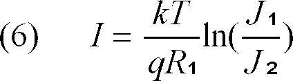
through transistor M4, where J₁ is the current density of transistor B1 and J₂ is the current density of transistor B2. - Transistor T1 is designed to generate a current that is N times the current flowing through transistor M4. As a result, the current contributed by current mirror A is:

where R₁ has been replaced by sheet resistance ρs and the number of squares r₁. In the preferred embodiment, the sheet resistance ρs for all of the resistors in the circuit will be the same. Therefore, the constant K₃ in equation (1) is as follows:
By scaling the current in the left and right legs of current mirror A, the need for a large number of bipolar structures (i.e., 30 or more) is eliminated. - Current mirror circuit B includes transistors M5-M8, transistor B3, and resistor R₂. Transistors M5 and M6 are p-channel MOSFETs, while transistors M7 and M8 are n-channel MOSFETs. Transistor B3 is a bipolar junction transistor.
- Resistor R₂ has one end connected to the drain of transistor M5 and a second end connected to power supply voltage V CC . The base and collector of transistor B3 also are connected to power supply voltage V CC while the sources of transistors M7 and M8 are connected to power supply voltage GND.
- Transistors M5-M8 and T2 are sized MOSFETs. Transistors M6 and M8 are scaled to generate a current flow that is one tenth of the current flowing through transistors M5 and M7. The current flowing through transistors M5 and M7 is equal to the current flowing through transistors M2 and M4 in current mirror A. Transistor T2 is constructed to provide a current flow that is M times the current flowing through transistor M7. The voltage VBE is set up by transistor B3 and resistor R₂ sets up the current; the voltage drop across R₂ is VBE. As a result, current mirror B generates a current:

where ρs is the sheet resistance of resistor R₂ and r₂ is the number of squares in resistor R₂. The constant K₂ from equation (1) is defined as:
- Next, current mirror C includes transistors M9-M15, and T3 and resistor R₃. Resistor R₃ has one end connected to the source of transistor M11 and another end connected to power supply voltage V CC . Transistor M9 has its source connected to power supply voltage V CC , while the sources of transistors M12, M13, and M14 are connected to ground power supply voltage GND. The voltage VT is set up by transistor M9, while resistor R₃ sets up the current. The voltage drop across R₃ is VT
- Transistors M9-M11, M15, and T3 are p-channel MOSFETs, while transistors M12-M14 are n-channel MOSFETs. These transistors are sized transistors. The current flowing through transistors M11 and M13 is the same as the current flowing through transistors M14 and M15. The current flowing through transistors M11 and M13-M15 is the same as the current flowing through transistor M5 and M7 in current mirror B. Transistors M9, M10, and M12 are sized to provide a current flow that is one tenth of the current flowing through transistors, M11, M13, M14, and M15. Transistor T3 is designed to provide a current flow that is L times the current flowing through transistor M14. Thus, current mirror C generates a current:

where ρ is the sheet resistance of resistor R₃ and r₃ is the number of squares in resistor R₃. The coefficient K₁ in equation (1) is defined as:
for current mirror C. - Current mirror D includes transistor M16, transistor T4, and resistor R₄. Both transistors M16 and T4 are p-channel MOSFETs with their sources connected power supply voltage V CC . Resistor R₄ has one end connected to the drain of transistor M16 and a second end connected to power supply voltage GND. Transistor M16 sets up the voltage V CC - VT, while resistor R₄ sets up the current. The voltage drop across R₄ is V CC -VT.
- Transistors M16 and T4 are scaled transistors. Transistor M16 is designed to provide a current flow that is equal to the current flowing through transistors M14 and M15; transistor T4 is constructed to generate a current that is J times the current flowing through transistor M16. Thus, the current generated by current mirror D is:

where the coefficient K₁ in the current mirror is set as:
Since both current mirrors C and D create current contributions that are related to the coefficient K₁, the current mirrors must be sized according the following relationship:
- As a result, the sum of the currents at node VSUM may be set equal to zero by the selection of the sizes and properties of the devices involved in constants K₁-K₃. The voltage at node OUT is set to VCC/2 in the depicted circuit when the voltage at VSUM is equal to VCC/2, and the power supply voltage V CC is equal to selected or threshold voltage. If the current from transistors T1 and T2 is greater than the current from transistors T3 and T4, the voltage at node OUT will swing up to that of power supply voltage V CC . This situation occurs when the power supply voltage V CC is greater than the selected voltage. On the other hand, if the current from transistors T1 and T2 is less than the current from transistors T3 and T4, the voltage at node OUT will swing down to that of power supply voltage GND. This situation occurs when the power supply voltage V CC is less than the selected or threshold voltage.
- The threshold voltage may be set at a value slightly less than the desired power supply voltage according to the present invention. For example, in a five volt power supply system, the threshold voltage may be set at 4.8 volts such that when the power supply is at 5 volts, the output at node OUT will swing up to power supply voltage V CC , 5 volts. If the power supply voltage drops below 4.8 volts, the output node OUT will swing down to the ground power supply voltage. Thus, through the selection of constants K₁-K₃, a voltage may be selected, wherein fluctuations of the power supply voltage V CC below the selected voltage will cause the comparator to indicate that a secondary or backup power supply should be switched to the circuit associated with the comparator.
- The MOSFETs used in the current mirrors in the depicted circuit may have longer channels than the base technology. For example, in a 0.8 micron device, the transistors used in the current mirrors may have channel lengths from 3 to 6 microns. These longer channels may be used improve the precision of the current supplied by the current mirrors.
- The scaling of currents in current mirrors A-D may be done in a variety of ways. In accordance with a preferred embodiment of the present invention, one of the transistors is selected as unity. A transistor that is to provide a current N times the current of the unity transistor is replaced with N unity transistors connected in parallel. Those of ordinary skill in the art will realize other methods of scaling currents may be employed.
- Next, the value of the resistors must match preset ratios when specified, but the actual magnitude of the resistors affects only the power consumption of the circuit.
- Current mirrors A-D in Figure 1 are an example of one layout of a DCSBV comparator in accordance with a preferred embodiment of the present invention. Other configurations for the current mirrors will be apparent to those of ordinary skill in the art. Other numbers of current mirror layouts may be employed to satisfy equation (1).
- Referring next to Figure 3, a schematic diagram of a DCSBV comparator is illustrated. This comparator is similar to the comparator depicted in Figure 1 with a few additional circuits. Drain impedance of the current sources may limit the voltage swing in some cases in which the current is limited to low or small changes. Additionally, small current changes may have problems in driving the node capacitance at node VSUM, resulting in a slow response.
- To solve these problems, a
cascode stage 24, well known to those of ordinary skill in the art, may be added the DCSBV comparator between the current sources and node VSUM, as depicted in Figure 2, to improve the switching speed of the circuit.Cascode stage 24 includes transistors E1-E6 and resistor R x . Transistors E1-E3 are p-channel MOSFETs, while transistors E4-E6 are n-channel MOSFETs. Transistor E2 has its source connected to power supply voltage V CC , while transistor E6 has its source connected to power supply voltage GND. Transistor E1 has its source connected to the drains of transistors T3 and T4; transistor E4 has its source connected to the drains of transistor T1 and T2. Transistors E1 and E4 have their drains connected to node VSUM. - In some instances, a selected voltage swing having a range other than that between the power supply voltage V CC and power supply voltage GND may be desired. A clamping
circuit 26, well known to those of ordinary skill in the art, may be added to provide a bias to set the voltage swing at node VSUM between selected or preset voltages. Clampingcircuit 26 includes transistors D1-D4 andinverter 30. Transistors D1 and D2 are n-channel MOSFETs, while transistors D3 and D4 are p-channel MOSFETs. Transistors D1 and D2 have their drains connected to power supply voltage V CC ; transistors D3 and D4 have their drains connected to ground power supply voltage GND. The sources of transistors D2 and D3 are connected to node VSUM. Other clamping circuits other than the one depicted also may be used with the comparator of the present invention. - In addition, a
hysteresis circuit 28, known to those of ordinary skill in the art, may be used to reduce the susceptibility of the comparator to noise from other components.Hysteresis circuit 28 includes transistors H1- H3. Transistors H1 and H2 are p-channel MOSFETs, and transistor H3 is an n-channel MOSFET. Transistor H1 has its source connected to power supply voltage V CC . The gate of transistor H1 is connected to the gate and source of transistor M16. The gate of transistor H2 is controlled by the output of inverter 34; the gate of transistor H3 is controlled by the output ofinverter 32.Inverters inverters - As a result, a DCSBV comparator provides an indicator for switching between a primary and secondary power supply without requiring a large number of devices for implementation as compared to a typical bandgap reference circuit. The present invention eliminates the need for using a large number of bipolar devices, large resistors, oscillators, switch capacitors, auto zero devices, etc. Through the use of current mirrors, the number of bipolar devices required are reduced. Additionally, sensitivity to noise also may be reduced by using a DCSBV comparator according to the present invention.
- Although the depicted embodiment employs for current mirrors, other numbers of current mirrors and current mirrors of other designs may be used as long as the implementation of the current mirrors performs the function of summing currents at a node. Additionally, more than one node may be used for summing currents.
- An example of typical values which can be used to fabricate an operational device are as follows. These numbers assume a typical processing technology, and a desired trip point for the comparator of approximately 4.4 volts. The constants K₁, K₂, and K₃, respectively, can be set to the values 2, 7, and 46 by proper selection of the various components and transistor sizes. Transistor design to give current densities of J₁ = 1.0 A/cm² and J² = 0.05 A/cm² provides for operation as described above.
- While the invention has been particularly shown and described with reference to a preferred embodiment, it will be understood by those skilled in the art that various changes in form and detail may be made therein without departing from the spirit and scope of the invention.
Claims (17)
a summing node;
a plurality of current sources connected to the summing node, each current source supplying a current to the summing node and being connected to a power supply voltage, wherein the current at the summing node is equal to zero when the power supply voltage is equal to a preselected voltage; and
an indicator circuit having an input connected to the summing node and generating a logical signal at an output, responsive to voltage changes in the summing node.
a first circuit;
a direct current sum bandgap voltage comparator comprising:
a summing node;
a plurality of current sources connected to the summing node, each current source supplying a current to the summing node and being connected to a power supply voltage, wherein the current at the summing node is equal to zero when the power supply voltage is equal to a preselected voltage; and
an indicator circuit having an input connected to the summing node and generating a logical signal at an output, responsive to changes in the summing node; and
a switching circuit for providing power to the first circuit from a primary power supply and a secondary power supply, the switching circuit being connected to the output of the indicator circuit, wherein power from the primary power supply is supplied to the first circuit if the logical signal indicates that the power supply voltage is equal to or greater than the preselected voltage and power from the secondary power supply is supplied to the first circuit if the power supply voltage is less than the preselected voltage.
Applications Claiming Priority (2)
| Application Number | Priority Date | Filing Date | Title |
|---|---|---|---|
| US5630193A | 1993-04-30 | 1993-04-30 | |
| US56301 | 1993-04-30 |
Publications (2)
| Publication Number | Publication Date |
|---|---|
| EP0627817A1 true EP0627817A1 (en) | 1994-12-07 |
| EP0627817B1 EP0627817B1 (en) | 1999-04-07 |
Family
ID=22003501
Family Applications (1)
| Application Number | Title | Priority Date | Filing Date |
|---|---|---|---|
| EP94303084A Expired - Lifetime EP0627817B1 (en) | 1993-04-30 | 1994-04-28 | Voltage comparator with bandgap based direct current summing and power supply switch using it |
Country Status (4)
| Country | Link |
|---|---|
| US (2) | US5781043A (en) |
| EP (1) | EP0627817B1 (en) |
| JP (1) | JPH0778481A (en) |
| DE (1) | DE69417622T2 (en) |
Cited By (2)
| Publication number | Priority date | Publication date | Assignee | Title |
|---|---|---|---|---|
| WO1997007409A1 (en) * | 1995-08-17 | 1997-02-27 | Advanced Micro Devices, Inc. | Vcc level detection circuit |
| WO1998057329A1 (en) * | 1997-06-12 | 1998-12-17 | Enable Semiconductor, Inc. | Voltage source and memory-voltage switch in a memory chip |
Families Citing this family (31)
| Publication number | Priority date | Publication date | Assignee | Title |
|---|---|---|---|---|
| DE19638087C2 (en) * | 1996-09-18 | 1999-09-02 | Siemens Ag | CMOS comparator |
| US5894423A (en) * | 1996-12-26 | 1999-04-13 | Motorola Inc. | Data processing system having an auto-ranging low voltage detection circuit |
| US5936392A (en) * | 1997-05-06 | 1999-08-10 | Vlsi Technology, Inc. | Current source, reference voltage generator, method of defining a PTAT current source, and method of providing a temperature compensated reference voltage |
| US6037833A (en) * | 1997-11-10 | 2000-03-14 | Philips Electronics North America Corporation | Generator for generating voltage proportional to absolute temperature |
| JP3954245B2 (en) | 1999-07-22 | 2007-08-08 | 株式会社東芝 | Voltage generation circuit |
| US6281734B1 (en) * | 1999-12-31 | 2001-08-28 | Stmicroelectronics, Inc. | Reference voltage adjustment |
| US6268764B1 (en) * | 2000-02-18 | 2001-07-31 | Microchip Technology Incorporated | Bandgap voltage comparator used as a low voltage detection circuit |
| TW479904U (en) * | 2000-10-09 | 2002-03-11 | Sunplus Technology Co Ltd | Diode circuit to simulate zero cutoff voltage and the rectifying circuit having zero cutoff voltage characteristics |
| US7665063B1 (en) | 2004-05-26 | 2010-02-16 | Pegasystems, Inc. | Integration of declarative rule-based processing with procedural programming |
| DE102004038552B4 (en) * | 2004-08-06 | 2006-05-11 | Atmel Germany Gmbh | voltage |
| US7116588B2 (en) * | 2004-09-01 | 2006-10-03 | Micron Technology, Inc. | Low supply voltage temperature compensated reference voltage generator and method |
| US20060164128A1 (en) * | 2005-01-21 | 2006-07-27 | Miller Ira G | Low current power supply monitor circuit |
| US8335704B2 (en) | 2005-01-28 | 2012-12-18 | Pegasystems Inc. | Methods and apparatus for work management and routing |
| US7633334B1 (en) * | 2005-01-28 | 2009-12-15 | Marvell International Ltd. | Bandgap voltage reference circuit working under wide supply range |
| KR100746293B1 (en) * | 2006-02-01 | 2007-08-03 | 삼성전자주식회사 | Cascode-type current mode comparator, receiver and semiconductor device having the same |
| US8924335B1 (en) | 2006-03-30 | 2014-12-30 | Pegasystems Inc. | Rule-based user interface conformance methods |
| US20090174392A1 (en) * | 2006-04-25 | 2009-07-09 | Nxp B.V. | Circuit arrangement and corresponding method for voltage reference and/or for current reference |
| US8250525B2 (en) | 2007-03-02 | 2012-08-21 | Pegasystems Inc. | Proactive performance management for multi-user enterprise software systems |
| FI20075322A0 (en) * | 2007-05-07 | 2007-05-07 | Nokia Corp | Power supplies for RF power amplifier |
| CN101557215B (en) * | 2008-07-07 | 2012-06-13 | 西安民展微电子有限公司 | Voltage comparator |
| US20100026375A1 (en) * | 2008-07-29 | 2010-02-04 | Texas Instruments Incorporated | Circuit to generate cmos level signal to track core supply voltage (vdd) level |
| US8027187B2 (en) * | 2008-09-12 | 2011-09-27 | Micron Technology, Inc. | Memory sensing devices, methods, and systems |
| US8843435B1 (en) | 2009-03-12 | 2014-09-23 | Pegasystems Inc. | Techniques for dynamic data processing |
| US8468492B1 (en) | 2009-03-30 | 2013-06-18 | Pegasystems, Inc. | System and method for creation and modification of software applications |
| US8880487B1 (en) | 2011-02-18 | 2014-11-04 | Pegasystems Inc. | Systems and methods for distributed rules processing |
| US9195936B1 (en) | 2011-12-30 | 2015-11-24 | Pegasystems Inc. | System and method for updating or modifying an application without manual coding |
| US10469396B2 (en) | 2014-10-10 | 2019-11-05 | Pegasystems, Inc. | Event processing with enhanced throughput |
| US10698599B2 (en) | 2016-06-03 | 2020-06-30 | Pegasystems, Inc. | Connecting graphical shapes using gestures |
| US10698647B2 (en) | 2016-07-11 | 2020-06-30 | Pegasystems Inc. | Selective sharing for collaborative application usage |
| US11048488B2 (en) | 2018-08-14 | 2021-06-29 | Pegasystems, Inc. | Software code optimizer and method |
| US11567945B1 (en) | 2020-08-27 | 2023-01-31 | Pegasystems Inc. | Customized digital content generation systems and methods |
Citations (12)
| Publication number | Priority date | Publication date | Assignee | Title |
|---|---|---|---|---|
| US4110677A (en) * | 1977-02-25 | 1978-08-29 | Beckman Instruments, Inc. | Operational amplifier with positive and negative feedback paths for supplying constant current to a bandgap voltage reference circuit |
| US4381458A (en) * | 1980-08-06 | 1983-04-26 | Racal Microelectronic Systems Limited | Back-up electrical power supplies |
| US4645943A (en) * | 1984-10-15 | 1987-02-24 | Dallas Semiconductor Corporation | Space-saving back-up power supply |
| US4654829A (en) * | 1984-12-17 | 1987-03-31 | Dallas Semiconductor Corporation | Portable, non-volatile read/write memory module |
| US4906863A (en) * | 1988-02-29 | 1990-03-06 | Texas Instruments Incorporated | Wide range power supply BiCMOS band-gap reference voltage circuit |
| US4935690A (en) * | 1988-10-31 | 1990-06-19 | Teledyne Industries, Inc. | CMOS compatible bandgap voltage reference |
| US5013941A (en) * | 1989-08-17 | 1991-05-07 | National Semiconductor Corporation | TTL to ECL/CML translator circuit |
| US5029295A (en) * | 1990-07-02 | 1991-07-02 | Motorola, Inc. | Bandgap voltage reference using a power supply independent current source |
| US5049807A (en) * | 1991-01-03 | 1991-09-17 | Bell Communications Research, Inc. | All-NPN-transistor voltage regulator |
| US5087831A (en) * | 1990-03-30 | 1992-02-11 | Texas Instruments Incorporated | Voltage as a function of temperature stabilization circuit and method of operation |
| US5103159A (en) * | 1989-10-20 | 1992-04-07 | Sgs-Thomson Microelectronics S.A. | Current source with low temperature coefficient |
| US5121539A (en) * | 1991-07-17 | 1992-06-16 | Trumpf Gmbh & Company | Apparatus and method for cutting stacked sheet-like workpieces |
Family Cites Families (16)
| Publication number | Priority date | Publication date | Assignee | Title |
|---|---|---|---|---|
| US3617859A (en) * | 1970-03-23 | 1971-11-02 | Nat Semiconductor Corp | Electrical regulator apparatus including a zero temperature coefficient voltage reference circuit |
| US4350904A (en) * | 1980-09-22 | 1982-09-21 | Bell Telephone Laboratories, Incorporated | Current source with modified temperature coefficient |
| US4473758A (en) * | 1983-02-07 | 1984-09-25 | Motorola Inc. | Substrate bias control circuit and method |
| US4556804A (en) * | 1983-11-17 | 1985-12-03 | Motorola, Inc. | Power multiplexer switch and method |
| US4617473A (en) * | 1984-01-03 | 1986-10-14 | Intersil, Inc. | CMOS backup power switching circuit |
| JPS63245236A (en) * | 1987-03-31 | 1988-10-12 | 株式会社東芝 | Electric source switching circuit |
| US5272393A (en) * | 1987-11-24 | 1993-12-21 | Hitachi, Ltd. | Voltage converter of semiconductor device |
| US4958123A (en) * | 1987-12-23 | 1990-09-18 | U.S. Philips Corporation | Circuit arrangement for processing sampled analogue electrical signals |
| US5121359A (en) | 1989-09-29 | 1992-06-09 | Sgs-Thomson Microelectronics, Inc. | Configuration memory for programmable logic device |
| US5111071A (en) * | 1989-10-19 | 1992-05-05 | Texas Instruments Incorporated | Threshold detection circuit |
| US5053640A (en) * | 1989-10-25 | 1991-10-01 | Silicon General, Inc. | Bandgap voltage reference circuit |
| US5034626A (en) * | 1990-09-17 | 1991-07-23 | Motorola, Inc. | BIMOS current bias with low temperature coefficient |
| US5336986A (en) * | 1992-02-07 | 1994-08-09 | Crosspoint Solutions, Inc. | Voltage regulator for field programmable gate arrays |
| JP3322685B2 (en) * | 1992-03-02 | 2002-09-09 | 日本テキサス・インスツルメンツ株式会社 | Constant voltage circuit and constant current circuit |
| US5373227A (en) * | 1993-03-26 | 1994-12-13 | Micron Semiconductor, Inc. | Control circuit responsive to its supply voltage level |
| US5774013A (en) * | 1995-11-30 | 1998-06-30 | Rockwell Semiconductor Systems, Inc. | Dual source for constant and PTAT current |
-
1994
- 1994-04-28 JP JP6092324A patent/JPH0778481A/en active Pending
- 1994-04-28 DE DE69417622T patent/DE69417622T2/en not_active Expired - Fee Related
- 1994-04-28 EP EP94303084A patent/EP0627817B1/en not_active Expired - Lifetime
-
1997
- 1997-09-18 US US08/932,930 patent/US5781043A/en not_active Ceased
-
2000
- 2000-07-14 US US09/616,821 patent/USRE39918E1/en not_active Expired - Lifetime
Patent Citations (13)
| Publication number | Priority date | Publication date | Assignee | Title |
|---|---|---|---|---|
| US4110677A (en) * | 1977-02-25 | 1978-08-29 | Beckman Instruments, Inc. | Operational amplifier with positive and negative feedback paths for supplying constant current to a bandgap voltage reference circuit |
| US4381458B1 (en) * | 1980-08-06 | 1995-04-11 | Dallas Semiconductor | Back-up electrical power supplies. |
| US4381458A (en) * | 1980-08-06 | 1983-04-26 | Racal Microelectronic Systems Limited | Back-up electrical power supplies |
| US4645943A (en) * | 1984-10-15 | 1987-02-24 | Dallas Semiconductor Corporation | Space-saving back-up power supply |
| US4654829A (en) * | 1984-12-17 | 1987-03-31 | Dallas Semiconductor Corporation | Portable, non-volatile read/write memory module |
| US4906863A (en) * | 1988-02-29 | 1990-03-06 | Texas Instruments Incorporated | Wide range power supply BiCMOS band-gap reference voltage circuit |
| US4935690A (en) * | 1988-10-31 | 1990-06-19 | Teledyne Industries, Inc. | CMOS compatible bandgap voltage reference |
| US5013941A (en) * | 1989-08-17 | 1991-05-07 | National Semiconductor Corporation | TTL to ECL/CML translator circuit |
| US5103159A (en) * | 1989-10-20 | 1992-04-07 | Sgs-Thomson Microelectronics S.A. | Current source with low temperature coefficient |
| US5087831A (en) * | 1990-03-30 | 1992-02-11 | Texas Instruments Incorporated | Voltage as a function of temperature stabilization circuit and method of operation |
| US5029295A (en) * | 1990-07-02 | 1991-07-02 | Motorola, Inc. | Bandgap voltage reference using a power supply independent current source |
| US5049807A (en) * | 1991-01-03 | 1991-09-17 | Bell Communications Research, Inc. | All-NPN-transistor voltage regulator |
| US5121539A (en) * | 1991-07-17 | 1992-06-16 | Trumpf Gmbh & Company | Apparatus and method for cutting stacked sheet-like workpieces |
Cited By (2)
| Publication number | Priority date | Publication date | Assignee | Title |
|---|---|---|---|---|
| WO1997007409A1 (en) * | 1995-08-17 | 1997-02-27 | Advanced Micro Devices, Inc. | Vcc level detection circuit |
| WO1998057329A1 (en) * | 1997-06-12 | 1998-12-17 | Enable Semiconductor, Inc. | Voltage source and memory-voltage switch in a memory chip |
Also Published As
| Publication number | Publication date |
|---|---|
| DE69417622D1 (en) | 1999-05-12 |
| DE69417622T2 (en) | 1999-09-09 |
| EP0627817B1 (en) | 1999-04-07 |
| USRE39918E1 (en) | 2007-11-13 |
| JPH0778481A (en) | 1995-03-20 |
| US5781043A (en) | 1998-07-14 |
Similar Documents
| Publication | Publication Date | Title |
|---|---|---|
| EP0627817A1 (en) | Direct current sum bandgap voltage comparator | |
| KR920005257B1 (en) | Stable current source circuit | |
| EP0360333B1 (en) | Temperature threshold sensing circuit | |
| US4477737A (en) | Voltage generator circuit having compensation for process and temperature variation | |
| US6329871B2 (en) | Reference voltage generation circuit using source followers | |
| US6894544B2 (en) | Brown-out detector | |
| US5481179A (en) | Voltage reference circuit with a common gate output stage | |
| US4849684A (en) | CMOS bandgap voltage reference apparatus and method | |
| US7208998B2 (en) | Bias circuit for high-swing cascode current mirrors | |
| US7994849B2 (en) | Devices, systems, and methods for generating a reference voltage | |
| US5280198A (en) | Power supply level detector | |
| EP0680048B1 (en) | Bandgap reference circuit | |
| US6476669B2 (en) | Reference voltage adjustment | |
| JP2001510609A (en) | Reference voltage source with temperature compensated output reference voltage | |
| US5627456A (en) | All FET fully integrated current reference circuit | |
| EP0786810B1 (en) | Substrate potential detecting circuit | |
| GB2265478A (en) | Reference voltage generating circuit | |
| EP0367578A1 (en) | CMOS compatible bandgap voltage reference | |
| KR100723474B1 (en) | Current mode comparator having hysteresis voltage | |
| JP2913428B2 (en) | Temperature sensor | |
| JP2000056846A (en) | Reference voltage generating circuit and semiconductor integrated circuit | |
| JP3263434B2 (en) | Constant voltage circuit | |
| JPH03222195A (en) | Sense amplification circuit | |
| JP2003015754A (en) | Reference voltage generating circuit | |
| JPH0869695A (en) | Semiconductor integrated circuit device |
Legal Events
| Date | Code | Title | Description |
|---|---|---|---|
| PUAI | Public reference made under article 153(3) epc to a published international application that has entered the european phase |
Free format text: ORIGINAL CODE: 0009012 |
|
| AK | Designated contracting states |
Kind code of ref document: A1 Designated state(s): DE FR GB IT |
|
| 17P | Request for examination filed |
Effective date: 19950513 |
|
| 17Q | First examination report despatched |
Effective date: 19961114 |
|
| GRAG | Despatch of communication of intention to grant |
Free format text: ORIGINAL CODE: EPIDOS AGRA |
|
| GRAG | Despatch of communication of intention to grant |
Free format text: ORIGINAL CODE: EPIDOS AGRA |
|
| GRAG | Despatch of communication of intention to grant |
Free format text: ORIGINAL CODE: EPIDOS AGRA |
|
| GRAH | Despatch of communication of intention to grant a patent |
Free format text: ORIGINAL CODE: EPIDOS IGRA |
|
| GRAH | Despatch of communication of intention to grant a patent |
Free format text: ORIGINAL CODE: EPIDOS IGRA |
|
| GRAA | (expected) grant |
Free format text: ORIGINAL CODE: 0009210 |
|
| RAP3 | Party data changed (applicant data changed or rights of an application transferred) |
Owner name: STMICROELECTRONICS, INC. |
|
| AK | Designated contracting states |
Kind code of ref document: B1 Designated state(s): DE FR GB IT |
|
| REF | Corresponds to: |
Ref document number: 69417622 Country of ref document: DE Date of ref document: 19990512 |
|
| ET | Fr: translation filed | ||
| PLBE | No opposition filed within time limit |
Free format text: ORIGINAL CODE: 0009261 |
|
| STAA | Information on the status of an ep patent application or granted ep patent |
Free format text: STATUS: NO OPPOSITION FILED WITHIN TIME LIMIT |
|
| 26N | No opposition filed | ||
| PGFP | Annual fee paid to national office [announced via postgrant information from national office to epo] |
Ref country code: DE Payment date: 20010423 Year of fee payment: 8 |
|
| REG | Reference to a national code |
Ref country code: GB Ref legal event code: IF02 |
|
| PG25 | Lapsed in a contracting state [announced via postgrant information from national office to epo] |
Ref country code: DE Free format text: LAPSE BECAUSE OF NON-PAYMENT OF DUE FEES Effective date: 20021101 |
|
| PGFP | Annual fee paid to national office [announced via postgrant information from national office to epo] |
Ref country code: FR Payment date: 20040408 Year of fee payment: 11 |
|
| PGFP | Annual fee paid to national office [announced via postgrant information from national office to epo] |
Ref country code: GB Payment date: 20040428 Year of fee payment: 11 |
|
| PG25 | Lapsed in a contracting state [announced via postgrant information from national office to epo] |
Ref country code: IT Free format text: LAPSE BECAUSE OF NON-PAYMENT OF DUE FEES;WARNING: LAPSES OF ITALIAN PATENTS WITH EFFECTIVE DATE BEFORE 2007 MAY HAVE OCCURRED AT ANY TIME BEFORE 2007. THE CORRECT EFFECTIVE DATE MAY BE DIFFERENT FROM THE ONE RECORDED. Effective date: 20050428 Ref country code: GB Free format text: LAPSE BECAUSE OF NON-PAYMENT OF DUE FEES Effective date: 20050428 |
|
| GBPC | Gb: european patent ceased through non-payment of renewal fee |
Effective date: 20050428 |
|
| PG25 | Lapsed in a contracting state [announced via postgrant information from national office to epo] |
Ref country code: FR Free format text: LAPSE BECAUSE OF NON-PAYMENT OF DUE FEES Effective date: 20051230 |
|
| REG | Reference to a national code |
Ref country code: FR Ref legal event code: ST Effective date: 20051230 |