EP0681235A2 - Device for summing up products of two equal or different signals - Google Patents
Device for summing up products of two equal or different signals Download PDFInfo
- Publication number
- EP0681235A2 EP0681235A2 EP95106093A EP95106093A EP0681235A2 EP 0681235 A2 EP0681235 A2 EP 0681235A2 EP 95106093 A EP95106093 A EP 95106093A EP 95106093 A EP95106093 A EP 95106093A EP 0681235 A2 EP0681235 A2 EP 0681235A2
- Authority
- EP
- European Patent Office
- Prior art keywords
- clock frequency
- signal
- adder
- output
- arrangement according
- Prior art date
- Legal status (The legal status is an assumption and is not a legal conclusion. Google has not performed a legal analysis and makes no representation as to the accuracy of the status listed.)
- Granted
Links
Images

Classifications
-
- G—PHYSICS
- G06—COMPUTING; CALCULATING OR COUNTING
- G06G—ANALOGUE COMPUTERS
- G06G7/00—Devices in which the computing operation is performed by varying electric or magnetic quantities
- G06G7/12—Arrangements for performing computing operations, e.g. operational amplifiers
- G06G7/16—Arrangements for performing computing operations, e.g. operational amplifiers for multiplication or division
- G06G7/161—Arrangements for performing computing operations, e.g. operational amplifiers for multiplication or division with pulse modulation, e.g. modulation of amplitude, width, frequency, phase or form
-
- G—PHYSICS
- G01—MEASURING; TESTING
- G01R—MEASURING ELECTRIC VARIABLES; MEASURING MAGNETIC VARIABLES
- G01R21/00—Arrangements for measuring electric power or power factor
- G01R21/133—Arrangements for measuring electric power or power factor by using digital technique
-
- G—PHYSICS
- G06—COMPUTING; CALCULATING OR COUNTING
- G06F—ELECTRIC DIGITAL DATA PROCESSING
- G06F7/00—Methods or arrangements for processing data by operating upon the order or content of the data handled
- G06F7/60—Methods or arrangements for performing computations using a digital non-denominational number representation, i.e. number representation without radix; Computing devices using combinations of denominational and non-denominational quantity representations, e.g. using difunction pulse trains, STEELE computers, phase computers
- G06F7/602—Methods or arrangements for performing computations using a digital non-denominational number representation, i.e. number representation without radix; Computing devices using combinations of denominational and non-denominational quantity representations, e.g. using difunction pulse trains, STEELE computers, phase computers using delta-sigma sequences
-
- G—PHYSICS
- G06—COMPUTING; CALCULATING OR COUNTING
- G06J—HYBRID COMPUTING ARRANGEMENTS
- G06J1/00—Hybrid computing arrangements
Landscapes
- Engineering & Computer Science (AREA)
- Physics & Mathematics (AREA)
- Theoretical Computer Science (AREA)
- General Physics & Mathematics (AREA)
- Mathematical Physics (AREA)
- Power Engineering (AREA)
- Software Systems (AREA)
- Computer Hardware Design (AREA)
- Mathematical Analysis (AREA)
- Computing Systems (AREA)
- Computational Mathematics (AREA)
- Mathematical Optimization (AREA)
- Pure & Applied Mathematics (AREA)
- General Engineering & Computer Science (AREA)
- Automation & Control Theory (AREA)
- Evolutionary Computation (AREA)
- Fuzzy Systems (AREA)
- Compression, Expansion, Code Conversion, And Decoders (AREA)
- Container Filling Or Packaging Operations (AREA)
- Beverage Vending Machines With Cups, And Gas Or Electricity Vending Machines (AREA)
Abstract
Description
Die Erfindung bezieht sich auf eine Anordnung zum Summieren von Produkten zweier gleichen oder unterschiedlichen Signale gemäss dem Oberbegriff des Anspruchs 1.The invention relates to an arrangement for summing products of two identical or different signals according to the preamble of
Die Anordnung wird verwendet, z. B. in Elektrizitätszählern, zum Ermitteln von Strom- und/oder Spannungs-Effektivwerten, Korrelationen, gemittelten elektrischen Leistungen und/oder Energiewerten. Die letzteren sind bekanntlich gleich einer Summe momentaner Leistungswerte, die ihrerseits jeweils gleich einem Produkt eines momentanen Spannungswertes und eines zugehörigen momentanen Stromwertes sind.The arrangement is used e.g. B. in electricity meters, for determining current and / or voltage rms values, correlations, averaged electrical powers and / or energy values. As is known, the latter are equal to a sum of instantaneous power values, which in turn are each a product of an instantaneous voltage value and an associated instantaneous current value.
Bekannt ist eine klassische Multiplikation, in der in einer langsamem Taktfrequenz zwei Operanden von je R Bits miteinander multipliziert werden, die z. B. zuerst vorher durch Filterung in einer schnelleren Taktfrequenz mit anschliessender Dezimation gewonnen wurden.A classic multiplication is known in which two operands of R bits each are multiplied with one another in a slow clock frequency. B. were first obtained beforehand by filtering in a faster clock frequency with subsequent decimation.
Der Erfindung liegt die Aufgabe zugrunde, unter mindestens annähernder Beibehaltung der mit der klassischen Multiplikation erreichbaren Genauigkeit, eine Anordnung der eingangs genannten Art zu realisieren, welche keine Multiplikation zweier R-Bit Operanden, sondern nur einfache Verschiebe- und algebraische Additions-Operationen in der schnelleren Taktfrequenz erfordern, wobei z. B. eine Berechnung eines Effektivwertes eines Stromes in einem Dynamikbereich von 1:1000 mit einer Genauigkeit von 0.5% ohne grossen Aufwand möglich ist. Die erfindungsgemässe Anordnung ist besonders vorteilhaft, wenn die Multiplikationen auf einem speziellen Halbleiter-Chip realisiert werden sollen.The invention is based, with at least approximately maintaining the accuracy achievable with classic multiplication, to realize an arrangement of the type mentioned at the outset which does not multiply two R-bit operands, but only simple shifting and algebraic addition operations in the faster Require clock frequency, z. B. a calculation of an effective value of a current in a dynamic range of 1: 1000 with an accuracy of 0.5% is possible with little effort. The arrangement according to the invention is particularly advantageous if the multiplications are to be implemented on a special semiconductor chip.
Die genannte Aufgabe wird erfindungsgemäss durch die im Kennzeichen des Anspruchs 1 angegebenen Merkmale gelöst. Vorteilhafte Ausgestaltungen der Erfindung ergeben sich aus den abhängigen Ansprüchen.According to the invention, this object is achieved by the features specified in the characterizing part of
Ausführungsbeispiele der Erfindung sind in der Zeichnung dargestellt und werden im folgenden näher beschrieben.Embodiments of the invention are shown in the drawing and are described in more detail below.
Es zeigen:
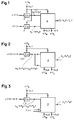
- Fig. 1
- ein Blockschaltbild einer ersten Variante einer erfindungsgemässen Anordnung,
- Fig. 2
- ein Blockschaltbild einer zweiten Variante der erfindungsgemässen Anordnung,
- Fig. 3
- ein Blockschaltbild einer dritten Variante der erfindungsgemässen Anordnung,
- Fig. 4
- ein Blockschaltbild eines bekannten Sigma-Delta-Modulators zweiter Ordnung und
- Fig. 5
- ein Blockschaltbild eines erfindungsgemässen Multiplizier/Addier-Gliedes.
- Fig. 1
- 2 shows a block diagram of a first variant of an arrangement according to the invention,
- Fig. 2
- 2 shows a block diagram of a second variant of the arrangement according to the invention,
- Fig. 3
- 2 shows a block diagram of a third variant of the arrangement according to the invention,
- Fig. 4
- a block diagram of a known second order sigma-delta modulator and
- Fig. 5
- a block diagram of an inventive multiplier / adder.
In den erfindungsgemässen Anordnungen wird jeweils ein erstes Signal u[t] bzw. i[t] mit einem zweiten gleichen oder unterschiedlichen Signal u[t] oder i[t] oder f[t] multipliziert. Dabei ist mindestens eines der Signale u[t] bzw. i[t] auf einen Signaleingang eines mit einer ersten Taktfrequenz 1/TS betriebenen Sigma-Delta-Modulators 1 bzw. 2 geführt, dessen Ausgang mit mindestens einem von zwei Signaleingängen eines Multiplizier/Addier-Gliedes 3 verbunden ist. Das Signal u[t] ist z. B. eine elektrische Spannung, während das Signal i[t] vorzugsweise eine elektrische Spannung darstellt, die proportional einem elektrischen Strom ist. Gehört letzterer zur Spannung u[t], dann ist das Produkt beider Signale u[t] und i[t] proportional der zugehörigen Momentanleistung ![]()
![]()
In der in der Fig. 1 dargestellten ersten Variante der erfindungsgemässen Anordnung sind die beiden Signale unterschiedliche zeitfunktionale Signale u[t] und i[t], die auf einen Signaleingang je eines zugehörigen, mit der ersten Taktfrequenz 1/TS betriebenen Sigma-Delta-Modulators 1 bzw. 2 geführt sind. Die Ausgänge der beiden Sigma-Delta-Modulatoren 1 und 2 sind dabei mit je einem der beiden Signaleingänge des Multiplizier/Addier-Gliedes 3 verbunden. Das zeitfunktionale Signal u[t] ist somit über den Sigma-Delta-Modulator 1 auf einen ersten der beiden Signaleingänge und das zeitfunktionale Signal i[t] über den Sigma-Delta-Modulator 2 auf einen zweiten der beiden Signaleingänge des Multiplizier/Addier-Gliedes 3 geführt.In the first variant of the arrangement according to the invention shown in FIG. 1, the two signals are different time-functional signals u [t] and i [t], which each have an associated sigma-delta operated at the
In der in der Fig. 2 dargestellten zweiten Variante der erfindungsgemässen Anordnung sind die beiden Signale gleiche zeitfunktionale Signale u[t] und u[t] bzw. i[t] und i[t], wovon eines auf den Signaleingang des Sigma-Delta-Modulators 1 bzw. 2 geführt ist. Der Ausgang des letzteren ist mit den beiden Signaleingängen des Multiplizier/Addier-Gliedes 3 verbunden. Die beiden gleichen zeitfunktionalen Signale u[t] und u[t] bzw. i[t] und i[t] werden in der erfindungsgemässen Anordnung so miteinander multipliziert, dass das Quadrat u²[t] bzw. i²[t] des betreffenden zeitfunktionalen Signals u[t] bzw. i[t] erzeugt wird.In the second variant of the arrangement according to the invention shown in FIG. 2, the two signals are the same time-functional signals u [t] and u [t] or i [t] and i [t], one of which relates to the signal input of the sigma-delta -
In der in der Fig. 3 dargestellten dritten Variante der erfindungsgemässen Anordnung ist das erste Signal ein im voraus nicht bekanntes zeitfunktionales Signal u[t] bzw. i[t] und das zweite Signal eine im voraus bekannte zeitvariable Funktion f[t]. Das erste Signal u[t] bzw. i[t] ist dabei auf den Signaleingang des zugehörigen Sigma-Delta-Modulators 1 bzw. 2 geführt. Der Ausgang des letzteren ist mit einem der beiden Signaleingänge des Multiplizier/Addier-Gliedes 3 verbunden. Einbit- oder Mehrbit-Digitalwerte der bekannten zeitvariablen Funktion f[t] sind ihrerseits auf den anderen der beiden Signaleingänge des Multiplizier/Addier-Gliedes 3 geführt. Die Werte der bekannten zeitvariablen Funktion f[t] stehen nicht immer in Gestalt eines 1-Bit Stromes zur Verfügung und werden dann über eine Busverbindung als Mehrbit-Digitalwerte dem betreffenden Signaleingang des Multiplizier/Addier-Gliedes 3 zugeführt, der dann als Bus-Eingang ausgebildet ist. In der Fig. 3 wird das Signal u[t] bzw. i[t] über den Sigma-Delta-Modulator 1 bzw. 2 als 1-Bit Strom dem ersten Signaleingang des Multiplizier/Addier-Gliedes 3 zugeführt, während z. B. Mehrbit-Digitalwerte der Funktion f[t] dem zweiten Signaleingang zugeführt sind. In der dritten Variante dient die Multiplikation/Addition z. B. der Ermittlung von Korrelationen.In the third variant of the arrangement according to the invention shown in FIG. 3, the first signal is a previously known time-functional signal u [t] or i [t] and the second signal is a previously known time-variable function f [t]. The first signal u [t] or i [t] is fed to the signal input of the associated sigma-
Das Multiplizier/Addier-Glied 3 ist in allen Varianten über getrennte Takteingänge mit drei Taktsignalen CL1, CL2 und CL3 gespeist. Die Sigma-Delta-Modulatoren 1 und 2 sind jeweils mit dem Taktsignal CL1 gespeist, dessen Frequenz die erste Taktfrequenz 1/TS ist. Die zeitfunktionalen Signale u[t] und i[t] werden im zugehörigen Sigma-Delta-Modulator 1 bzw. 2 mit der ersten Taktfrequenz 1/TS abgetastet. Die Frequenz von CL2 ist die zweite Taktfrequenz 1/TM und diejenige von CL3 die dritte Taktfrequenz 1/TL. Es gilt TS < TM < TL, mit ![]()
![]()
![]()
![]()
![]()
![]()
![]()
![]()
Nachfolgend bezeichnen hTS, kTM und jTL die zu der Taktfrequenz 1/TS bzw. 1/TM bzw. 1/TL gehörigen Abtastzeitpunkte, wobei h, k und j laufende Abtastnummem n = 0, 1, 2, 3, ..., usw. darstellen. Signale der Taktfrequenz 1/TS besitzen nachfolgend einen Index S, Signale der Taktfrequenz 1/TM einen Index M und ein Signal der Taktfrequenz 1/TL einen Index L. Dementsprechend sind die Ausgangssignale der Sigma-Delta-Modulatoren 1 und 2 mit xS[hTS] bzw. yS[hTS] und das Ausgangssignal des Multiplizier/Addier-Gliedes 3 mit zL[jTL] bezeichnet (Siehe Fig. 1 bis Fig. 3).In the following, hT S , kT M and jT L denote the sampling times belonging to the
Der Aufbau und die Arbeitsweise der Sigma-Delta-Modulatoren 1 und 2 sind aus der Druckschrift tm, Technisches Messen 59 (1992) Hefte 1,2,6 und 7/8, Seiten 262 bis 268, Anwendung von Oversampling-Verfahren zur Erhöhung der Auflösung digital erfasster Signale, M. Barmettler und P. Gruber, R. Oldenbourg Verlag, bekannt, welche nachfolgend als Barmettler et al bezeichnet wird.The structure and mode of operation of the sigma-
Jeder Sigma-Delta-Modulator 1 bzw. 2 der drei erfindungsgemässen Varianten ist vorzugsweise ein Sigma-Delta-Modulator zweiter Ordnung. In der Fig. 4 ist ein solcher, an sich bekannter Sigma-Delta-Modulator 1 bzw. 2 zweiter Ordnung dargestellt, dessen Vorwärtspfad in der angegebenen Reihenfolge aus einer Reihenschaltung eines ersten Differenzbildungs-Gliedes 4, eines ersten Verstärkungsgliedes 5, eines ersten Integrators 6, eines zweiten Differenzbildungs-Gliedes 7, eines zweiten Verstärkungsgliedes 8, eines zweiten Integrators 9 und eines 1-Bit Analog/Digital-Wandlers 10 besteht, wobei letzterer vorzugsweise ein getasteter Komparator ist und bei den beiden Differenzbildungs-Gliedern 4 und 7 für die Reihenschaltung jeweils der Plus-Eingang verwendet wird. Der Ausgang des 1-Bit Analog/Digital-Wandlers 10, der gleichzeitig der Ausgang des Sigma-Delta-Modulators 1 bzw. 2 ist, ist über einen 1-Bit Digital/Analog-Wandler 11, z. B. ein Halteglied nullter Ordnung ("Zero order hold" ZOH) mit den Minus-Eingängen der beiden Differenzbildungs-Glieder 4 und 7 verbunden. Ein Takteingang des 1-Bit Analog/Digital-Wandlers 10 wird vom Taktsignal CL1 mit der ersten Taktfrequenz 1/TS gespeist. In den Verstärkungsgliedern 5 und 8 werden deren Eingangssignale mit einem Faktor K₁ bzw. K₂ gewichtet.Each sigma-
Für das Ausgangssignal xS[hTS] des Sigma-Delta Modulators 1 gilt:![]()

![]()
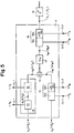
Wie in der Fig. 5 dargestellt ist innerhalb des Multiplizier/Addier-Gliedes 3 der eine, z. B. zweite Signaleingang über ein mit der ersten Taktfrequenz 1/TS betriebenes erstes Dezimationsfilter 12 auf einen ersten Eingang eines Additionsgliedes 13 und der andere, z. B. erste Signaleingang über eine mit der ersten Taktfrequenz 1/TS betriebene Verzögerungsanordnung 14 auf einen zweiten Eingang des Additionsgliedes 13 geführt. Bei der Multiplikation der Spannung u[t] mit dem zugehörigen Strom i[t] zwecks Ermittlung der Summe entsprechender Momentanleistungen (Siehe Fig. 1) wird das Signal i[t], welches in der Regel einen grösseren Dynamikbereich besitzt als die Spannung u[t], vorzugsweise dem zweiten Signaleingang des Multiplizier/Addier-Gliedes 3 und damit dem Dezimationsfilter 12 zugeführt, während die Spannung u[t] vorzugsweise dem ersten Signaleingang, d. h. der Verzögerungsanordnung 14 zugeführt wird. Die Genauigkeit ist dabei besser als diejenige bei der Ermittlung der Effektivwerte des Stromes i[t] (Siehe Fig. 2), da die grosse Dynamik nur bei einem Operanden, nämlich dem Strom i[t] vorhanden ist. In der dritten Variante (Siehe Fig. 3) wird das Signal u[t] bzw. i[t] vorzugsweise dem ersten Signaleingang des Multiplizier/Addier-Gliedes 3 und damit der Verzögerungsanordnung 14 zugeführt, während die z. B. Mehrbit-Digitalwerte der Funktion f[t] vorzugsweise dem zweiten Signaleingang und damit dem Dezimationsfilter 12 zugeführt werden.As shown in Fig. 5 is within the multiplier /
Das Additionsglied 13 dient der Realisation algebraischer Additionen und sein Ausgang ist über ein Dividierglied 17 auf einen Signaleingang eines mit der zweiten Taktfrequenz 1/TM betriebenen zweiten Dezimationsfilters 18 geführt, dessen Ausgang einen Ausgang des Multiplizier/Addier-Gliedes 3 bildet. Der Teilungsfaktor des Dividiergliedes 17 ist gleich dem Verhältnis TM/TS der schnellen ersten Taktfrequenz 1/TS des Taktsignals CL1 zur mittelschnellen zweiten Taktfrequenz 1/TM des Taktsignals CL2, d. h. gleich der ersten Überabtastrate N.The
Die Dezimationsfilter 12 und 18 sind definitionsgemäss Digitalfilter, deren Ausgangssignal mit einer niedrigeren Taktfrequenz ausgelesen wird als mit welcher ihr Eingangssignal im eigentlichen Digitalfilter verarbeitet wird. Dies ist in der Fig. 5 symbolisch angedeutet, indem dort die Dezimationsfilter 12 und 18 jeweils durch einen Eingangs-Funktionsblock 12a bzw. 18a und einen nachgeschalteten Ausgangs-Funktionsblock 12b bzw. 18b dargestellt sind. Die Eingangs-Funktionsblöcke 12a und 18a stellen jeweils das eigentliche Digitalfilter dar, während die Ausgangs-Funktionsblöcke 12b und 18b den Auslesevorgang andeuten, der jeweils durch einen Lese-Schaltkontakt 12c bzw. 18c symbolisch dargestellt ist. Der Eingangs-Funktionsblock 12a besitzt einen Takteingang, der vom Taktsignal CL1 mit der schnellen ersten Taktfrequenz 1/TS gespeist ist, während der Ausgangs-Funktionsblock 12b einen Takteingang aufweist, der vom Taktsignal CL2 mit einer langsameren, nämlich der mittelschnellen zweiten Taktfrequenz 1/TM gespeist ist. Der Eingangs-Funktionsblock 18a besitzt einen Takteingang, der vom Taktsignal CL2 mit der mittelschnellen zweiten Taktfrequenz 1/TM gespeist ist, während der Ausgangs-Funktionsblock 18b einen Takteingang aufweist, der vom Taktsignal CL3 mit der langsamen dritten Taktfrequenz 1/TL gespeist ist. Die Ausgangs-Funktionsblöcke 12b und 18b der Dezimationsfilter 12 und 18 werden somit mit einer niedrigeren Taktfrequenz 1/TM bzw. 1/TL betrieben als der zugehörige Eingangs-Funktionsblock 12a bzw. 18a, welcher mit der Taktfrequenz 1/TS bzw. 1/TM betrieben wird, wobei die zweite Taktfrequenz 1/TM und die dritte Taktfrequenz 1/TL jeweils dem Lesen des Ausgangssignals des ersten bzw. zweiten Dezimationsfilters 12 bzw. 18 dienen.By definition, the decimation filters 12 and 18 are digital filters, the output signal of which is read out with a lower clock frequency than the one with which their input signal is processed in the actual digital filter. This is indicated symbolically in FIG. 5 in that the decimation filters 12 and 18 are each represented by an
Das Dezimationsfilter 12 ist vorzugsweise ein Sinc-Filter der Ordnung K und der Länge N, d. h. seine Länge ist vorzugsweise gleich der ersten Überabtastrate N, also gleich dem Verhältnis TM/TS der schnellen ersten Taktfrequenz 1/TS zur mittelschnellen zweiten Taktfrequenz 1/TM. Es gelten z. B. K = 3 und N = 128. Das Dezimationsfilter 18 ist vorzugsweise ein Sinc-Filter erster Ordnung der Länge W, d. h. seine Länge ist vorzugsweise gleich der zweiten Überabtastrate W, also gleich dem Verhältnis TL/TM der mittelschnellen zweiten Taktfrequenz 1/TM zur langsamen dritten Taktfrequenz 1/TL.The
Ein mit der Taktfrequenz 1/TS betriebenes Sinc-Filter der Ordnung K und der Länge N hat bekanntlich einen Frequenzgang
und ein solches Filter erster Ordnung ist vorzugsweise ein Mittelwertbildner, der z. B. aus einem N-stufigen Schieberegister besteht, dessen Eingang und dessen N Parallelausgänge auf je einen von N+1 Eingängen eines gemeinsamen Addiergliedes geführt sind, wobei der Ausgang des letzteren über ein Dividierglied, dessen Teilungsfaktor N ist, auf den Ausgang des Mittelwertbildners und damit auch auf den Ausgang des Sinc-Filters geführt ist.A Sinc filter of order K and length N operated with the
and such a first-order filter is preferably an averager, e.g. B. consists of an N-stage shift register, the input and the N parallel outputs of which are routed to one of N + 1 inputs of a common adder, the output of the latter via a divider, whose division factor is N, to the output of the averager and so that it is also led to the output of the sinc filter.
Die Verzögerungsanordnung 14 besteht entweder aus einem mit der ersten Taktfrequenz 1/TS betriebenen Verzögerungsglied 15 oder aus einer Reihenschaltung 15;16 des mit der ersten Taktfrequenz 1/TS betriebenen Verzögerungsgliedes 15 und eines nachgeschalteten, ebenfalls mit der ersten Taktfrequenz 1/TS betriebenen dezimationslosen Digitalflters 16. Je ein Takteingang des Verzögerungsgliedes 15 und, falls vorhanden, des Digitalfilters 16 wird vom Taktsignal CL1 mit der schnellen Taktfrequenz 1/TS gespeist. Das nur fakultative Vorhandensein des Digitalfilters 16 ist in der Fig. 5 symbolisch angedeutet durch seine gestrichelte Darstellung. Das dezimationslose Digitalfilter 16 ("sliding filter") ist vorzugsweise ein Sinc-Filter erster Ordnung der Länge vier.The
Das schnell getaktete Signal xS[hTS] wird im Verzögerungsglied 15 um eine Verzögerungsdauer D verzögert, so dass an dessen Ausgang ein schnell getaktetes verzögertes Signal dS[hTS] erscheint. Die Verzögerungsdauer D des Verzögerungsgliedes 15 ist vorzugsweise gleich K(N-1)/2. Wenn ein Digitalfilter 16 vorhanden ist, wird das schnell getaktete verzögerte Signal dS[hTS] ausserdem noch durch Tiefpassfilterung im Digitalfilter 16 in ein tiefpassgefiltertes verzögertes Signal vS[hTS] umgewandelt, wodurch ein gegenüber der schnellen Taktfrequenz 1/TS tieffrequentes Nutzsignal herausgefiltert und das Quantisierungsrauschen teilweise unterdrückt wird.The rapidly clocked signal x S [hT S ] is delayed in the
Im Dezimationsfilter 12 wird der 1-Bit-Strom yS[hTS] der schnellen Taktfrequenz 1/TS tiefpassgefiltert und auf die langsamere mittelschnelle Taktfrequenz ![]()
![]()
Je grösser die erste Überabtastrate N gewählt wird, desto stärker ist die Unterdrückung des Quantisierungseinflusses und desto grösser ist auch die Genauigkeit des gewandelten Signals. Wird der Quantisierungsfehler des 1-Bit Analog/Digital-Wandlers 10 als idealisiertes, im Intervall [-Q/2,Q/2] gleichverteiltes Rauschen betrachtet, so ist dessen Varianz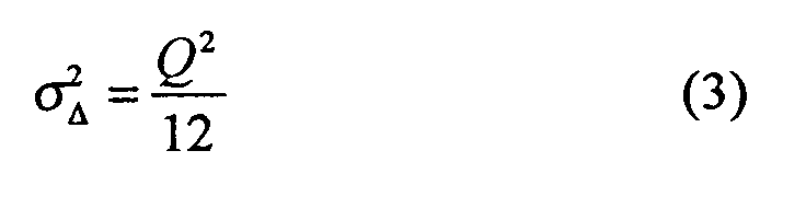
Für die linearisierte Übertragung des Quantisierungsfehlers ist die Störübertragungsfunktion des Sigma-Delta-Modulators zweiter Ordnung gleich:![]()
Die Varianz des Quantisierungsfehlers am Ausgang des Sigma-Delta-Modulators 2 ist:
Am Ausgang des Dezimationsfilters 12 ist das Signal![]()

Zu beachten ist, dass z⁻¹ die Verzögerung im schnellen Takt 1/TS ist. Für N = 4 gilt z.B.:
Die Differenzengleichungen für K = 1, K = 2 und K = 3 ergeben jeweils:![]()
![]()
in der langsameren mittelschnellen Taktfrequenz 1/TM gilt:![]()
Drei Dinge sind von Interesse:
- 1) Die Summe aller Gewichte vonist immer

gleich 1, d.h. die Gleichstrom-Verstärkung ist gleich 1. - 2) Das
Gedächtnis des Dezimationsfilters 12 ist abhängig von dessen Ordnung K. Nur im Falle von K = 1 ist das Gedächtnis gleich N-1, was bedeutet, dass in diesem Fall das Gedächtnis gerade über die Länge eines langsamen Abtastintervalls reicht. Für K > 1 gilt allgemein:

- 3) Die Gewichte haben eine spezielle Struktur, nämlich für
- K = 1:
- rechtecksförmig,
- K = 2:
- dreiecksförmig und
- K = 3:
- parabolförmig mit einem abgeflachten Mittelstück.
Dasdie mittelschnelle Taktfrequenz 1/TM aufweisende Signal yM[kTM] hat einen Quantisierungsfehler ΔMi[kTM], der sich aus der Reihenschaltung des Sigma-Delta-Modulators 2 und des Dezimationsfilters 12 ergibt (Siehe Barmettler et al). Für interessante Werte von N und K ergibt sich folgender Gewinn Ri an Bits gegenüber dem nichtdezimierten Fall:
Für N = 128, K = 2 --> Ri=12.7Bits,
für N = 128, K = 3 --> Ri=15 Bits,
für N = 256, K = 2 --> Ri=14.7Bits und
für N = 256, K = 3--> Ri=17.5Bits.
For the linearized transmission of the quantization error, the interference transfer function of the second-order sigma-delta modulator is the same:
The variance of the quantization error at the output of the sigma-
The signal is at the output of the decimation filter 12
It should be noted that the delay in the fast cycle is 1 / T S. For example, for N = 4:
The difference equations for K = 1, K = 2 and K = 3 each result in:
in the slower medium-
Three things are of interest:
- 1) The sum of all weights of is always equal to 1, ie the direct current gain is equal to 1.
- 2) The memory of the
decimation filter 12 depends on its order K. Only in the case of K = 1 is the memory equal to N-1, which means that in this case that Memory extends just over the length of a slow sampling interval. The following generally applies for K> 1: - 3) The weights have a special structure, namely for
- K = 1:
- rectangular,
- K = 2:
- triangular and
- K = 3:
- parabolic with a flattened middle section.
The signal y M [kT M ] having the medium-fast clock frequency 1 / T M has a quantization error Δ Mi [kT M ], which results from the series connection of the sigma-delta modulator 2 and the decimation filter 12 (see Barmettler et al). For interesting values of N and K, the following gain R i of bits results compared to the non-decimated case:
For N = 128, K = 2 -> R i = 12.7 bits,
for N = 128, K = 3 -> R i = 15 bits,
for N = 256, K = 2 -> R i = 14.7 bits and
for N = 256, K = 3 -> R i = 17.5 bits.
Das heisst, dass die statistisch ermittelten, als gleichverteilt angenommenen Fehleramplituden am Ausgang des Dezimationsfilters 12 um den Faktor![]()
kleiner sind.
Beispiel: Bei N = 128 und K = 3 gilt![]()
![]()
![]()
are smaller.
Example: With N = 128 and K = 3 applies ![]()
![]()
Die Verzögetung der Reihenschaltung 15;16 sollte möglichst gut der durch das Dezimationsfilter 12 verursachten Verzögerung angepasst sein. Eine möglichst kleine Verzögerung ist vom Implementationsaufwand her von Vorteil. Das Signal am Ausgang des Verzögerungsgliedes 15 ist:![]()
![]()
Die Reihenschaltung 15;16 des Verzögerungsgliedes 15 und des Digitalfilters 16 arbeitet immer im schnellen Takt 1/TS. Zu bemerken ist, dass das Digitalfilter 16 als sogenanntes "Sliding filter" arbeitet und keine Dezimation auf die langsamere mittelschnelle Taktfrequenz 1/TM durchgeführt wird.The delay of the ![]()
![]()
The
Für das Nutzsignal gilt in der Reihenschaltung 15;16 ähnliches wie im Falle des Dezimationsfilters 12. Es sind aber andere Verzerrungen vorhanden. Der zu erwartende Quantisierungsfehler ist nicht nur verschieden, sondern auch viel grösser, da nur eine bescheidene Filterung des Quantisierungsrauschens erfolgt.The same applies to the useful signal in the
Wenn das Digitalfilter 16 z.B. ein "Sliding"-Sinc-Filter erster Ordnung der Länge vier ist, ist die Ausgangssequenz v S [hT S ] des Digitalfilters 16 sehr einfach, obwohl eine günstige Filterwirkung erzielt wird. Für die Übertragung gilt:![]()
![]()
Für die linearisierte Übertragung des Quantisierungsfehlers![]()
zum Ausgang des Digitalfilters 16 ergibt sich:
Daraus berechnet sich die Rauschleistung des Quantisierungsfehlers![]()
am Ausgang des Digitalfilters 16 zu
Für den Bitgewinn ergibt sich in diesem Fall
Die maximale Fehleramplitude bei angenommener Gleichverteilung reduziert sich somit nur um einen Faktor 2.
Das am Ausgang des Dezimationsfilters 12 erhaltene mittelschnelle Signal yM[kTM] wird im Additionsglied 13 mit dem schnellen Signal v S [hT S ] der Taktfrequenz 1/TS angesteuert. Da letzteres im gewählten Beispiel nur die Werte +1, +1/2, 0, -1/2 und -1 annehmen kann, müssen im Additionsglied 13 nur die Operationen "Verschieben", "Addiere/Subtrahiere (+1/2, -1/2)" und "Addiere/Subtrahiere (+1, -1)" durchgeführt werden. Im Additionsglied 13 werden somit Verschiebungen und algebraische Additionen mit anschliessender Dezimation auf die langsame Taktfrequenz 1/TM durchgeführt. Das Additionsglied 13 hat dabei die Aufgabe, das während N schnellen Takten der Frequenz 1/TS konstante, vom Dezimationsfilter 12 herkommende Signal yM[kTM] richtig anzusteuern. Anhand von zwei Beispielen soll der Vorgang erläutert werden.
- a) Beispiel 1: Multiplikation von u[t] mit sich selber, d. h.


Unter Berücksichtigung der Gleichung (9a) für yM[kTM] ergibt sich:
im Dividierglied 17 durch N geteilt, so dass am Ausgang des letzteren folgendes Signal zM[kTM] ansteht:
- b) Beispiel 2: Multiplikation von u[t] mit sich selber, d. h.

for the output of the digital filter 16:
The noise power of the quantization error is calculated from this
at the output of the
In this case, the bit gain results
The maximum error amplitude with assumed equal distribution is therefore reduced by a factor of 2.
The medium-fast signal y M [kT M ] obtained at the output of the
- a) Example 1 : Multiplication of u [t] with itself, ie
digital filter 16, ie with
Taking into account the equation (9a) for y M [kT M ], the following results:adder 13 in thedivider 17 is divided by N, so that the following signal z M [kT M ] is present at the output of the latter: - b) Example 2 : Multiplication of u [t] with itself, ie
digital filter 16, which is a first order sliding filter of length four.
Unter Berücksichtigung der Gleichung (9b) für yM[kTM] und der Gleichung (9a) für vS[hTS] ergibt sich:
Nach N Operationen wird das Ausgangssignal des Additionsgliedes 13 wiederum im Dividierglied 17 durch N geteilt, so dass am Ausgang des letzteren folgendes Signal zM[kTM] ansteht:
Es ist ersichtlich, dass die Wirkung des Additionsgliedes 13 wiederum eine Quadrierung des Ausgangssignals yM[kTM] des Dezimationsfilters 12 ist.After N operations, the output signal of the
It can be seen that the effect of the
Das Ausgangssignal zM[kTM] des Dividiergliedes 17 ist somit, wenn ![]()
![]()
![]()
![]()
Falls das Signal u[t] oder i[t] mit sich selber multipliziert wird, erscheint am Ausgang des Multiplizer/Addier-Gliedes 3 das Quadrat des Effektivwertes des betreffenden Signals u[t] bzw. i[t]. Falls nicht das Quadrat des Effektivwertes, sondern der Effektivwert selber ermittelt werden soll, ist der Ausgang des Multiplizier/Addier-Gliedes 3 mit einem Eingang eines Quadratwurzelziehungs-Gliedes 19 (Siehe Fig. 5) verbunden. Anschliessend an die Dezimierung auf die langsame Taktfrequenz 1/TL im zweiten Dezimationsfilter 18 wird im Quadratwurzelziehungs-Glied 19 aus dem Ausgangssignal zL[jTL] des zweiten Dezimationsfilters 18 durch Quadratwurzelziehen z. B. der Effektivwert Ueff des zeitfunktionalen Signals u[t] ermittelt. Das Quadratwurzelziehen im Quadratwurzelziehungs-Glied 19 erfolgt mit der langsamen Taktfrequenz 1/TL.If the signal u [t] or i [t] is multiplied by itself, the square of the effective value of the relevant signal u [t] or i [t] appears at the output of the multiplier /
Claims (14)
Applications Claiming Priority (3)
| Application Number | Priority Date | Filing Date | Title |
|---|---|---|---|
| CH01411/94A CH689471A5 (en) | 1994-05-05 | 1994-05-05 | Summer for products of similar or different signals e.g. for electricity meter |
| CH141194 | 1994-05-05 | ||
| CH1411/94 | 1994-05-05 |
Publications (3)
| Publication Number | Publication Date |
|---|---|
| EP0681235A2 true EP0681235A2 (en) | 1995-11-08 |
| EP0681235A3 EP0681235A3 (en) | 1995-12-27 |
| EP0681235B1 EP0681235B1 (en) | 2001-12-05 |
Family
ID=4209825
Family Applications (1)
| Application Number | Title | Priority Date | Filing Date |
|---|---|---|---|
| EP95106093A Expired - Lifetime EP0681235B1 (en) | 1994-05-05 | 1995-04-24 | Device for summing up products of two equal or different signals |
Country Status (5)
| Country | Link |
|---|---|
| US (1) | US5745063A (en) |
| EP (1) | EP0681235B1 (en) |
| AT (1) | ATE210312T1 (en) |
| CH (1) | CH689471A5 (en) |
| DE (1) | DE59509893D1 (en) |
Cited By (6)
| Publication number | Priority date | Publication date | Assignee | Title |
|---|---|---|---|---|
| EP0782035A1 (en) | 1995-12-29 | 1997-07-02 | Xerox Corporation | Method of forming array of light active cells and array |
| EP0782036A1 (en) | 1995-12-29 | 1997-07-02 | Xerox Corporation | Array of cells with light active circuitry |
| WO1998002838A1 (en) * | 1996-07-12 | 1998-01-22 | Analog Devices, Inc. | A four quadrant multiplying apparatus and method |
| DE19630605A1 (en) * | 1996-07-29 | 1998-02-05 | Tech Gmbh Antriebstechnik Und | Multiplication circuit for power measuring device |
| WO1998013699A1 (en) * | 1996-09-25 | 1998-04-02 | Siemens Aktiengesellschaft | Electrical power measuring device and method |
| CN103091550A (en) * | 2013-01-08 | 2013-05-08 | 北京优科利尔能源设备有限公司 | Synchronous isolation sampling direct-current power meter of wide voltage and large current |
Families Citing this family (7)
| Publication number | Priority date | Publication date | Assignee | Title |
|---|---|---|---|---|
| US6396877B1 (en) * | 1998-01-27 | 2002-05-28 | Agere Systems Guardian Corp. | Method and apparatus for combining serial data with a clock signal |
| EP1365515B1 (en) * | 2002-05-22 | 2006-10-18 | Freescale Semiconductor, Inc. | Analog-to-digital converter arrangement and method |
| DE10311777B4 (en) * | 2003-03-18 | 2005-10-20 | Thomas Schoch | Method, measuring system and device for electrical power measurement |
| US8180169B2 (en) * | 2008-02-27 | 2012-05-15 | Xerox Corporation | System and method for multi-scale sigma filtering using quadrature mirror filters |
| EP2263355B1 (en) * | 2008-03-31 | 2012-09-12 | Nxp B.V. | High resolution digital modulator by switching between discrete PWM or PPM values |
| US8208753B2 (en) * | 2008-04-11 | 2012-06-26 | Xerox Corporation | Method and system for noise level detection in image data |
| US9525430B1 (en) * | 2015-12-03 | 2016-12-20 | Djuro G. Zrilic | Method and apparatus for full-wave rectification of delta-sigma modulated signals |
Citations (1)
| Publication number | Priority date | Publication date | Assignee | Title |
|---|---|---|---|---|
| GB2167619A (en) * | 1984-11-24 | 1986-05-29 | Crest Energy Scan Ltd | Wattmeter circuit |
Family Cites Families (6)
| Publication number | Priority date | Publication date | Assignee | Title |
|---|---|---|---|---|
| JP3012887B2 (en) * | 1989-03-13 | 2000-02-28 | 日本テキサス・インスツルメンツ株式会社 | Signal converter |
| JP2832619B2 (en) * | 1989-09-29 | 1998-12-09 | ジーイー横河メディカルシステム株式会社 | Digital RF type ultrasonic diagnostic equipment |
| US5148167A (en) * | 1990-04-06 | 1992-09-15 | General Electric Company | Sigma-delta oversampled analog-to-digital converter network with chopper stabilization |
| US5208594A (en) * | 1991-05-02 | 1993-05-04 | Ricoh Company, Ltd. | Signal processor that uses a delta-sigma modulation |
| JP3104108B2 (en) * | 1992-09-07 | 2000-10-30 | ソニー株式会社 | Analog / digital converter |
| US5625358A (en) * | 1993-09-13 | 1997-04-29 | Analog Devices, Inc. | Digital phase-locked loop utilizing a high order sigma-delta modulator |
-
1994
- 1994-05-05 CH CH01411/94A patent/CH689471A5/en not_active IP Right Cessation
-
1995
- 1995-04-24 DE DE59509893T patent/DE59509893D1/en not_active Expired - Lifetime
- 1995-04-24 AT AT95106093T patent/ATE210312T1/en active
- 1995-04-24 EP EP95106093A patent/EP0681235B1/en not_active Expired - Lifetime
-
1997
- 1997-06-02 US US08/867,205 patent/US5745063A/en not_active Expired - Lifetime
Patent Citations (1)
| Publication number | Priority date | Publication date | Assignee | Title |
|---|---|---|---|---|
| GB2167619A (en) * | 1984-11-24 | 1986-05-29 | Crest Energy Scan Ltd | Wattmeter circuit |
Non-Patent Citations (1)
| Title |
|---|
| IEEE JOURNAL OF SOLID-STATE CIRCUITS, Bd. 26, Nr. 12, Dezember 1991 NEW YORK US, Seiten 2008-2015, XP 000272862 S. GARVERICK 'A Programmable Mixed-Signal ASIC for Power Metering' * |
Cited By (8)
| Publication number | Priority date | Publication date | Assignee | Title |
|---|---|---|---|---|
| EP0782035A1 (en) | 1995-12-29 | 1997-07-02 | Xerox Corporation | Method of forming array of light active cells and array |
| EP0782036A1 (en) | 1995-12-29 | 1997-07-02 | Xerox Corporation | Array of cells with light active circuitry |
| WO1998002838A1 (en) * | 1996-07-12 | 1998-01-22 | Analog Devices, Inc. | A four quadrant multiplying apparatus and method |
| DE19630605A1 (en) * | 1996-07-29 | 1998-02-05 | Tech Gmbh Antriebstechnik Und | Multiplication circuit for power measuring device |
| WO1998013699A1 (en) * | 1996-09-25 | 1998-04-02 | Siemens Aktiengesellschaft | Electrical power measuring device and method |
| US6239589B1 (en) | 1996-09-25 | 2001-05-29 | Siemens Aktiengesellschaft | Method and device for compensating for angle errors when measuring electrical power |
| CN103091550A (en) * | 2013-01-08 | 2013-05-08 | 北京优科利尔能源设备有限公司 | Synchronous isolation sampling direct-current power meter of wide voltage and large current |
| CN103091550B (en) * | 2013-01-08 | 2015-02-11 | 北京优科利尔能源设备有限公司 | Synchronous isolation sampling direct-current power meter of wide voltage and large current |
Also Published As
| Publication number | Publication date |
|---|---|
| EP0681235A3 (en) | 1995-12-27 |
| DE59509893D1 (en) | 2002-01-17 |
| ATE210312T1 (en) | 2001-12-15 |
| CH689471A5 (en) | 1999-04-30 |
| US5745063A (en) | 1998-04-28 |
| EP0681235B1 (en) | 2001-12-05 |
Similar Documents
| Publication | Publication Date | Title |
|---|---|---|
| EP0052847B1 (en) | Method and circuit for converting the sampling frequency of a series of samples avoiding conversion into a continuous signal | |
| DE69938338T2 (en) | DIRECT DIGITAL SYNTHETIZER FOR ANGLE MODULATION | |
| DE3120914C2 (en) | ||
| DE4203879A1 (en) | METHOD FOR CONVERTING A MEASURING SIGNAL AND A REFERENCE SIGNAL TO AN OUTPUT SIGNAL, AND CONVERTER FOR IMPLEMENTING THE METHOD | |
| EP0681235B1 (en) | Device for summing up products of two equal or different signals | |
| DE19733397B4 (en) | Feedback band-pass delta sigma converter with tunable center frequency | |
| DE2728939A1 (en) | DEVICE AND METHOD FOR SELECTIVELY MEASURING INTERMODULATION DISTORTION | |
| DE69631420T2 (en) | METHOD AND DEVICE FOR ESTIMATING NONLINEARITY | |
| DE3124924A1 (en) | RECURSIVE DIGITAL LOW-PASS FILTER | |
| DE2403233B2 (en) | ||
| DE2831059C2 (en) | Integrating code converter | |
| DE3705209C2 (en) | ||
| EP0215810B1 (en) | Circuit for obtaining an average value | |
| DE3621737C2 (en) | ||
| DE19521610B4 (en) | Decimation filter using a zero fill circuit to provide a selectable decimation ratio and decimation filtering method | |
| DE69932673T2 (en) | Digital signal synthesizer | |
| DE4303356A1 (en) | Digital phase locked loop | |
| DE102011116217A1 (en) | Use of a multilevel pulse width modulated signal for real time noise cancellation | |
| DE2804915C2 (en) | ||
| DE19510655B4 (en) | Circuit arrangement for filtering a stream of quantized electrical signals and method for filtering a stream of quantized electrical signals | |
| DE19510656B4 (en) | Circuit arrangement and method for filtering quantized electrical signals | |
| DE60205297T2 (en) | Method and apparatus for generating a random signal with controlled histogram and spectrum | |
| DE3922469C2 (en) | ||
| DE3621446A1 (en) | DEVICE FOR DIGITAL PROCESSING OF CONTINUOUS BIT FLOWS | |
| EP0339037B1 (en) | Non-recursive half-band filter |
Legal Events
| Date | Code | Title | Description |
|---|---|---|---|
| PUAI | Public reference made under article 153(3) epc to a published international application that has entered the european phase |
Free format text: ORIGINAL CODE: 0009012 |
|
| PUAL | Search report despatched |
Free format text: ORIGINAL CODE: 0009013 |
|
| AK | Designated contracting states |
Kind code of ref document: A2 Designated state(s): AT CH DE FR GB LI |
|
| AK | Designated contracting states |
Kind code of ref document: A3 Designated state(s): AT CH DE FR GB LI |
|
| 17P | Request for examination filed |
Effective date: 19960201 |
|
| RAP1 | Party data changed (applicant data changed or rights of an application transferred) |
Owner name: SIEMENS METERING AG |
|
| 17Q | First examination report despatched |
Effective date: 20000704 |
|
| GRAG | Despatch of communication of intention to grant |
Free format text: ORIGINAL CODE: EPIDOS AGRA |
|
| GRAG | Despatch of communication of intention to grant |
Free format text: ORIGINAL CODE: EPIDOS AGRA |
|
| GRAH | Despatch of communication of intention to grant a patent |
Free format text: ORIGINAL CODE: EPIDOS IGRA |
|
| GRAH | Despatch of communication of intention to grant a patent |
Free format text: ORIGINAL CODE: EPIDOS IGRA |
|
| GRAA | (expected) grant |
Free format text: ORIGINAL CODE: 0009210 |
|
| AK | Designated contracting states |
Kind code of ref document: B1 Designated state(s): AT CH DE FR GB LI |
|
| REF | Corresponds to: |
Ref document number: 210312 Country of ref document: AT Date of ref document: 20011215 Kind code of ref document: T |
|
| REG | Reference to a national code |
Ref country code: CH Ref legal event code: EP |
|
| REG | Reference to a national code |
Ref country code: GB Ref legal event code: IF02 |
|
| GBT | Gb: translation of ep patent filed (gb section 77(6)(a)/1977) |
Effective date: 20011211 |
|
| REF | Corresponds to: |
Ref document number: 59509893 Country of ref document: DE Date of ref document: 20020117 |
|
| ET | Fr: translation filed | ||
| PLBE | No opposition filed within time limit |
Free format text: ORIGINAL CODE: 0009261 |
|
| STAA | Information on the status of an ep patent application or granted ep patent |
Free format text: STATUS: NO OPPOSITION FILED WITHIN TIME LIMIT |
|
| 26N | No opposition filed | ||
| REG | Reference to a national code |
Ref country code: CH Ref legal event code: PFA Owner name: LANDIS+GYR AG Free format text: SIEMENS METERING AG#FELDSTRASSE 1#6300 ZUG (CH) -TRANSFER TO- LANDIS+GYR AG#FELDSTRASSE 1#6300 ZUG (CH) |
|
| REG | Reference to a national code |
Ref country code: CH Ref legal event code: NV Representative=s name: OK PAT AG PATENTE MARKEN LIZENZEN |
|
| REG | Reference to a national code |
Ref country code: FR Ref legal event code: CD |
|
| REG | Reference to a national code |
Ref country code: CH Ref legal event code: NV Representative=s name: RENTSCH & PARTNER |
|
| REG | Reference to a national code |
Ref country code: CH Ref legal event code: PCAR Free format text: RENTSCH & PARTNER;FRAUMUENSTERSTRASSE 9, POSTFACH 2441;8022 ZUERICH (CH) |
|
| REG | Reference to a national code |
Ref country code: CH Ref legal event code: PFA Owner name: LANDIS+GYR AG Free format text: LANDIS+GYR AG#FELDSTRASSE 1#6300 ZUG (CH) -TRANSFER TO- LANDIS+GYR AG#FELDSTRASSE 1#6300 ZUG (CH) |
|
| REG | Reference to a national code |
Ref country code: CH Ref legal event code: NV Representative=s name: WEINMANN ZIMMERLI, CH |
|
| PGFP | Annual fee paid to national office [announced via postgrant information from national office to epo] |
Ref country code: GB Payment date: 20140430 Year of fee payment: 20 |
|
| PGFP | Annual fee paid to national office [announced via postgrant information from national office to epo] |
Ref country code: AT Payment date: 20140425 Year of fee payment: 20 Ref country code: FR Payment date: 20140428 Year of fee payment: 20 Ref country code: CH Payment date: 20140425 Year of fee payment: 20 Ref country code: DE Payment date: 20140627 Year of fee payment: 20 |
|
| REG | Reference to a national code |
Ref country code: CH Ref legal event code: PCOW Free format text: NEW ADDRESS: THEILERSTRASSE 1, 6301 ZUG (CH) |
|
| REG | Reference to a national code |
Ref country code: DE Ref legal event code: R071 Ref document number: 59509893 Country of ref document: DE |
|
| REG | Reference to a national code |
Ref country code: CH Ref legal event code: PL |
|
| REG | Reference to a national code |
Ref country code: GB Ref legal event code: PE20 Expiry date: 20150423 |
|
| REG | Reference to a national code |
Ref country code: AT Ref legal event code: MK07 Ref document number: 210312 Country of ref document: AT Kind code of ref document: T Effective date: 20150424 |
|
| PG25 | Lapsed in a contracting state [announced via postgrant information from national office to epo] |
Ref country code: GB Free format text: LAPSE BECAUSE OF EXPIRATION OF PROTECTION Effective date: 20150423 |