EP1766421B1 - A method and an apparatus for measuring voltage on a conductor in a power switching device - Google Patents
A method and an apparatus for measuring voltage on a conductor in a power switching device Download PDFInfo
- Publication number
- EP1766421B1 EP1766421B1 EP05762595A EP05762595A EP1766421B1 EP 1766421 B1 EP1766421 B1 EP 1766421B1 EP 05762595 A EP05762595 A EP 05762595A EP 05762595 A EP05762595 A EP 05762595A EP 1766421 B1 EP1766421 B1 EP 1766421B1
- Authority
- EP
- European Patent Office
- Prior art keywords
- conductor
- power switching
- capacitors
- switching device
- voltage
- Prior art date
- Legal status (The legal status is an assumption and is not a legal conclusion. Google has not performed a legal analysis and makes no representation as to the accuracy of the status listed.)
- Not-in-force
Links
- 238000000034 method Methods 0.000 title claims abstract description 13
- 239000004020 conductor Substances 0.000 title claims description 26
- 239000003990 capacitor Substances 0.000 claims abstract description 47
- 239000000463 material Substances 0.000 claims description 6
- 239000000945 filler Substances 0.000 claims description 3
- 239000004593 Epoxy Substances 0.000 claims description 2
- 229910052782 aluminium Inorganic materials 0.000 claims description 2
- XAGFODPZIPBFFR-UHFFFAOYSA-N aluminium Chemical compound [Al] XAGFODPZIPBFFR-UHFFFAOYSA-N 0.000 claims description 2
- 239000011248 coating agent Substances 0.000 claims description 2
- 238000000576 coating method Methods 0.000 claims description 2
- 239000004814 polyurethane Substances 0.000 claims description 2
- 229920002635 polyurethane Polymers 0.000 claims description 2
- 238000009826 distribution Methods 0.000 description 13
- 238000004804 winding Methods 0.000 description 8
- 230000007175 bidirectional communication Effects 0.000 description 4
- 230000005611 electricity Effects 0.000 description 4
- 238000004519 manufacturing process Methods 0.000 description 4
- 230000003321 amplification Effects 0.000 description 3
- 230000006854 communication Effects 0.000 description 3
- 238000004891 communication Methods 0.000 description 3
- 238000010586 diagram Methods 0.000 description 3
- 238000003199 nucleic acid amplification method Methods 0.000 description 3
- 238000010248 power generation Methods 0.000 description 3
- CWYNVVGOOAEACU-UHFFFAOYSA-N Fe2+ Chemical group [Fe+2] CWYNVVGOOAEACU-UHFFFAOYSA-N 0.000 description 2
- 238000012423 maintenance Methods 0.000 description 2
- 238000012545 processing Methods 0.000 description 2
- 238000012546 transfer Methods 0.000 description 2
- 230000002159 abnormal effect Effects 0.000 description 1
- 238000006243 chemical reaction Methods 0.000 description 1
- 238000005520 cutting process Methods 0.000 description 1
- 238000001514 detection method Methods 0.000 description 1
- 238000009434 installation Methods 0.000 description 1
- 229910052751 metal Inorganic materials 0.000 description 1
- 239000002184 metal Substances 0.000 description 1
- 238000012544 monitoring process Methods 0.000 description 1
- 230000001681 protective effect Effects 0.000 description 1
- 238000005070 sampling Methods 0.000 description 1
- 230000001360 synchronised effect Effects 0.000 description 1
Images
Classifications
-
- G—PHYSICS
- G01—MEASURING; TESTING
- G01R—MEASURING ELECTRIC VARIABLES; MEASURING MAGNETIC VARIABLES
- G01R15/00—Details of measuring arrangements of the types provided for in groups G01R17/00 - G01R29/00, G01R33/00 - G01R33/26 or G01R35/00
- G01R15/04—Voltage dividers
- G01R15/06—Voltage dividers having reactive components, e.g. capacitive transformer
-
- G—PHYSICS
- G01—MEASURING; TESTING
- G01R—MEASURING ELECTRIC VARIABLES; MEASURING MAGNETIC VARIABLES
- G01R19/00—Arrangements for measuring currents or voltages or for indicating presence or sign thereof
- G01R19/145—Indicating the presence of current or voltage
- G01R19/15—Indicating the presence of current
-
- G—PHYSICS
- G01—MEASURING; TESTING
- G01R—MEASURING ELECTRIC VARIABLES; MEASURING MAGNETIC VARIABLES
- G01R15/00—Details of measuring arrangements of the types provided for in groups G01R17/00 - G01R29/00, G01R33/00 - G01R33/26 or G01R35/00
- G01R15/14—Adaptations providing voltage or current isolation, e.g. for high-voltage or high-current networks
- G01R15/16—Adaptations providing voltage or current isolation, e.g. for high-voltage or high-current networks using capacitive devices
-
- G—PHYSICS
- G01—MEASURING; TESTING
- G01R—MEASURING ELECTRIC VARIABLES; MEASURING MAGNETIC VARIABLES
- G01R15/00—Details of measuring arrangements of the types provided for in groups G01R17/00 - G01R29/00, G01R33/00 - G01R33/26 or G01R35/00
- G01R15/14—Adaptations providing voltage or current isolation, e.g. for high-voltage or high-current networks
- G01R15/18—Adaptations providing voltage or current isolation, e.g. for high-voltage or high-current networks using inductive devices, e.g. transformers
- G01R15/181—Adaptations providing voltage or current isolation, e.g. for high-voltage or high-current networks using inductive devices, e.g. transformers using coils without a magnetic core, e.g. Rogowski coils
Abstract
Description
- This application claims the priority of
U.S. provisional patent application Ser. No. 60/581,451 filed on June 21, 2004 - The present invention relates to a power switching device and more particularly to a method of measuring voltage potential levels in a power switching device.
- In the power generation and distribution industry, utility companies generate and distribute electricity to customers. To facilitate the process of distributing electricity, various types of power switching devices are used. In a distribution circuit, electricity flows through the power switching devices from a power generation source (a substation or the like) to the consumer. When a fault is detected in the distribution circuit, the power switching device is opened and the electrical connection is broken.
- Various controllers and protective relays are used by the utility company to detect faults that occur in the distribution circuit. This most controllers use a microprocessor programmed to respond to the fault based on the type of fault and the type of power switching device connected to the controller. The controller may respond to a particular fault by causing the power switching device to open. Alternatively, upon the detection of a fault, the controller may cause the power switching device to open and close multiple times.
- In order to make the most efficient switching in the distribution circuit and isolate the fault, the controllers need to monitor both the voltage present at the power switching device and electrical current flowing through the power switching device. If the amount of current exceeds a preprogrammed threshold for a certain period of time, the controller instructs the power switching device to perform the preprogrammed response. Should the fault continue to persist, the power switching device opens and remains open.
- Monitoring the voltage levels at the power switching device is essential for determining, for example, the direction of power flow, if the power switching device is being back-fed, or if the three phases of power are synchronized. Additionally, the utility personnel can use this information to monitor the output and efficiency of the distribution transformers providing power through the power switching devices. Presently, utility company personnel monitor voltage levels present at the power switching device by using dedicated potential transformers that are connected to the power switchingdevices. The controllers sample the output of the potential transformers and report this information to the craftsperson or other utility personnel. Voltage levels may be monitored at both the input connector and the output connector of the power switching device.
- Using a dedicated potential transformer as a voltage measuring device is cumbersome and expensive because each voltage phase must be monitored separately. If voltage is measured at both connectors, two dedicated potential transformers are required per phase and there may not be enough room on the utility pole for each of the potential transformers. One solution is to use a voltage divider circuit connected to a conductor of a power device. The voltage divider circuit can be designed to include resistors or capacitors. Typically, the voltage drop over a divider load impedance (low voltage leg) is measured with respect to a voltage drop over a reference impedance (high voltage leg). From this ratio a value of the voltage potential is determined.
- The use of a capacitive voltage divider in a power switching device to measure voltage is described in
US Pat No. 4,074,193 ("the '193 patent") . The '193 patent discloses the use of a separate cylindrical conductor as an electrode forming in part the high voltage leg of a capacitive voltage divider. The corresponding voltage from the low voltage leg of the capacitive voltage divider is amplified and sent to a voltage potential measuring device, meter or controller. -
US patent 4,963,819 discloses a high voltage capacitor suitable for measuring the voltage of an overhead power line. The capacitor may be enclosed in A casing which can contain one or more current transformers; the casing houses also a contact assembly whose voltage potential has to be measured. The elements of the contact assembly form the inner electrode of the capacitor whose outer electrode is provided by an additional cylindrical metal electrode. - The present invention eliminates the need for a separate dedicated conductor for the high voltage leg of the capacitive voltage divider. The present invention instead uses an existing shield of a current measuring device such as, for example, a transformer or Rogowski coil in the power switching device. The capacitive relationship between the shield and the high voltage conductor form the high voltage leg of the capacitive voltage divider. By using the existing shield, the cost of the separate conductor is eliminated. The present invention also allows the capacitive voltage divider to be tuned to thereby provide greater accuracy in measuring the voltage potential at the power switching device.
- A method of determining a voltage potential on a conductor in a power switching device as defined in claim 1.
- A voltage potential measuring apparatus for measuring a voltage potential on a conductor in a power switching device as defined in claim 5.
- The invention is further described in the detailed description that follows, by reference to the noted drawings by way of non-limiting illustrative embodiments of the invention, in which like reference numerals represent similar elements throughout the several views of the drawings, and wherein:
-
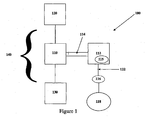
Figure 1 illustrates a block diagram of a typical power switching configuration. -
Figure 2 illustrates a cross sectional view of a recloser used in the power generation and distribution industry. -
Figure 3 illustrates an exploded cross sectional view of a current transformer installed in the power switching device. -
Figure 4 illustrates a schematic diagram of a capacitive voltage divider circuit in accordance with one embodiment of the present invention. -
Figure 1 shows a block diagram of a typicalpower switching configuration 100. Thepower switching configuration 100 has apower switching device 110 which is connected in series between apower source 120 and aload 130. The electrical circuit between thepower source 120 and theload 130 is referred to as thepower distribution circuit 140. Thepower switching device 110 is connected to acontroller 112 by abidirectional communications bus 114. Amicroprocessor 115 provides thecontroller 112 with the processing capability to monitor thepower switching device 110 for faults as well as operating conditions. In the preferred embodiment, a Motorola HC12D60 microprocessor is used. Auser 118 configures thecontroller 112 and receives information from thecontroller 112 via auser interface 116. Theuser interface 116 connects to thecontroller 112 through a communication means 122. Thedistribution circuit 140 is shown as a single phase of a three phase circuit for ease of illustration. The other two phases are identical. - The
power switching device 110 connects thepower source 120 to theload 130. Apower source 120 used with the present invention is a substation that provides, for example, a 1 kilovolt(kV) up to 40kV source of three phase AC power. An individual distribution transformer or bank of transformers connected together comprises theload 130. The transformers may be three phase transformers for large industrial applications or single phase transformers used to provide electricity to a residential consumer. - Three types of
power switching devices 110 that utility companies use in thepower switching configuration 100 are fault interrupters, breakers and reclosers. Eachpower switching device 110 performs a preprogrammed response when a fault condition in thepower distribution circuit 140 is detected by thecontroller 112. For example, the fault interrupter opens once and remains open when a fault condition is detected. The breaker opens after a fault, but attempts to close before remaining open if the fault continues to exist. A recloser opens and closes multiple times when a fault condition exists. By opening and closing multiple times, the recloser attempts to clear the fault. Should the fault condition continue to exist, the recloser opens and remains open until reset manually. The recloser enters a "lock out" state when this occurs. - A fault condition occurs when one phase of power becomes shorted to ground, phases become shorted to each other, or when lightning strikes the
distribution circuit 140. When a fault condition occurs, large amounts of current flow through thepower distribution circuit 140. Thecontroller 112 monitors the voltage and current levels communicated to it by thepower switching device 110. Thepower switching device 110 sends this information to thecontroller 112 through thebidirectional communications bus 114. When an abnormal current level is detected by thecontroller 112, thecontroller 112 signals thepower switching device 110 to execute the preprogrammed response. Twoexample controllers 112 used with the present invention are the ICD (Intelligent Control Device) and the PCD (Programmable Control Device), manufactured by ABB Inc. - A
user 118 may be the utility craftsperson who is at the power switching device location. The craftsperson can use a laptop PC as theuser interface 116 and connect directly to a serial port on thecontroller 112. The connection to the serial port is the communication means 122. Anotheruser 118 may be the utility maintenance person remotely logged into thecontroller 112. In this example, the remotely located utility maintenance person uses a desktop PC for theuser interface 116 and a modem configuration as the communication means 122 to connect to thecontroller 112. - A cross sectional view of a typical
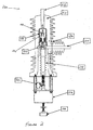
power switching device 110 in the form of arecloser 200 such as the OVR 1 Single Phase Recloser manufactured by ABB Inc. is illustrated inFigure 2 . Current flows through therecloser 200 from anH1 connector 212, through avacuum interrupter 230 and acurrent transfer assembly 224 to anH2 connector 214. Thevacuum interrupter 230 provides an enclosure that houses astationary contact 232 and amoveable contact 234. Thestationary contact 232 is directly connected to theH1 connector 212. Thecurrent transfer assembly 224 provides the electrical connection between themoveable contact 234 and theH2 connector 214. - Mounted around the
H2 connector 214 is acurrent transformer 236. Thecurrent transformer 236 provides a current to thecontroller 112 that is proportional to the current flowing through theH2 connector 214. Thecontroller 112 samples the proportional current and determines an appropriate value which is in turn conveyed to theuser 118 through theuser interface 116. - A cross-sectional view of the
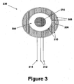
current transformer 236 along the axis X-X ofFigure 2 is shown inFigure 3 . Thecurrent transformer 236 has wire wound around an annular shapedferrous core 306 to form a winding 308. The winding 308 andmagnetic core 306 are encased in anelectrostatic shield 310. In one embodiment, conductive tape or semi-conductive tape is used for theelectrostatic shield 310. In another embodiment, the electrostatic shield is an aluminum coating applied to thecore 306 and winding 308. In between theH2 connector 214 and thecurrent transformer 236 is a layer offiller material 304 such as epoxy or polyurethane. This is the same material that is used for thehousing 210 of therecloser 200. - The
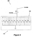
current transformer 236 is electrically connected to thebidirectional communications bus 114 by the two windingleads 312 and theshield lead 314. The winding leads 312 are connected to the winding 308 and theshield lead 314 is connected to theshield 310. Thebidirectional communications bus 114 routes the electrical signals from the winding leads 312 and theshield lead 314 to thecontroller 112 for processing. Inside thecontroller 112, the signals from the winding leads 312 are connected to a current sensing circuit (not shown) and the signal from theshield lead 314 is connected to a capacitivevoltage divider circuit 400, one embodiment of which is shown inFig. 4 . - The
layer 304 between thecurrent transformer 236 and theH2 conductor 214 provides a consistent and predictable dielectric property between theshield 310 and theH2 connector 214. The combination of theshield 310, thelayer 304, and theH2 connector 214 form a capacitor C1 which is shown in the schematic ofFigure 4 . The capacitor C1 forms a high voltage leg of thecapacitive voltage divider 400. In the previously described OVR-1recloser 200, the capacitance of C1 is approximately 30-50 pF. - As shown in
Figure 4 , theshield lead 314 connects to thelow voltage leg 404 of thecapacitive voltage divider 400. In this embodiment, thelow voltage leg 404 comprises individual capacitors C2-C21, which are connected between theshield 310 and ground. Removing one or more of the capacitors C2-C21 allows thecapacitive voltage divider 400 to be tuned. This is explained in further detail in subsequent sections. Alternatively, should thecapacitive voltage divider 400 not need to be adjusted, the capacitors C2-C21 may be combined into one single capacitor. - Within the
controller 112, the output voltage Vout across thelow voltage leg 404 is sent to an amplification stage (not shown) and then to an analog to digital converter circuit stage (not shown). In a preferred embodiment, themicroprocessor 115 has several built-in A/D converters which are connected to the amplification stage. Themicroprocessor 115 determines the appropriate voltage potential value from the output of the A/D converter and that value is displayed to auser 118 via theuser interface 116. - In a preferred embodiment, the capacitors C2-C21 of the
low voltage leg 404 are mounted on a printed circuit board (not shown) within thecontroller 112 and are easily accessible by manufacturing personnel or a craftsperson. In this embodiment, the capacitors C4-C21 may be removed by breaking or cutting them off the printed circuit board while capacitors C2 and C3 are not removable. Removing one or all of the capacitors C4-C21 reduces the total capacitance of thelow voltage leg 404 and increases the value of the output voltage Vout. The values of the capacitors C4-C21 are chosen to allow thecapacitive voltage divider 400 to be tuned with as much granularity as possible. In one exemplarycapacitive voltage divider 400 based on the capacitance of C1 being approximately 40pF, the capacitance for each of capacitors C2-C21 and the percent change in Vout resulting from removal of each of capacitors C4-C21 are shown in the table below.Capacitors Value Percentage Change C2, C3 0.1 µF Non-Removable C4-C7 0.033 µF 7.5% C8-C15 0.01 µF 2% C16-21 3300 pF .76% - The
voltage divider 400 is tuned to account for any variance in the capacitance of the high voltage leg C1. for the embodiment ofFigure 4 , the tuned capacitance ratio of thelow voltage leg 404 to the high voltage leg C1 is approximately 10,000:1. This ratio was chosen to provide the controller circuitry (amplification stage and A/D conversion stage) with an AC voltage within a sampling area. Those skilled in the art appreciate that this ratio is also a de-facto industry standard. As an illustrative example, should thelow voltage leg 404 of thecapacitive voltage divider 400 need to be tuned down by 18.5%, capacitors C4, C5, C8, C16 and C17 are removed and the output voltage Vout increases by 18.5%. - As discussed previously, the capacitors C4-21 within the
controller 112 are accessible to manufacturing or utility personnel. During the manufacturing and assembly process, thecontroller 112 may be paired with apower switching device 110. In this case, the capacitivevoltage divider circuitry 400 may be adjusted for the unique capacitance value C1 of thepower switching device 110 prior to shipment. The manufacturing person measures the capacitance of C1 and then removes the appropriate capacitors C4-C21 to achieve the 10,000:1 ratio. If thecontroller 112 is shipped to the field separately, the utility craftsperson may tune thevoltage divider 400 at the installation site performing the same steps prior to bringing thepower switching device 110 on line. - The present invention may also be applied to
power switching devices 110 using other types of shielded coils for use in measuring current and voltage, such as shielded Rogowski coils. Those skilled in the art appreciate that the Rogowski coil is an air core toroidal coil placed around a conductor. The core of the Rogowski coil is constructed of a non-ferrous material. An alternating magnetic field within the coil, produced by the current flowing in the conductor, induces a voltage which is proportional to the rate of change of the current. The output of the Rogowski coil is sent to an integrator where the value of voltage is extrapolated. The voltage measured with the Rogowski coil is a function of the amount of current flowing through thepower switching device 110. - While the Rogowski coil is not shown in any of the drawing figures,
Figure 4 does show the shield lead 406 of the Rogowski coil and the conductor 408 around which the air core toroidal coil of the Rogowski coil is placed. The capacitor C1 ofcircuit 400 is formed from the combination of the shield of the Rogowski coil, the conductor 408 and the air core there between. In this embodiment, the air core is the dielectric of capacitor C1. Thelow voltage leg 404 of thecapacitive voltage divider 400 is designed with the appropriate values for capacitors C2-C21 to provide the preferred ratio of 10,000:1. The present invention measures the voltage potential at the conductor 408 independentof the amount of current flowing through thepower switching device 110. - It is to be understood that the foregoing description has been provided merely for the purpose of explanation and is in no way to be construed as limiting of the invention. Where the invention has been described with reference to embodiments, it is understood that the words which have been used herein are words of description and illustration, rather than words of limitation. Further, although the invention has been described herein with reference to particular structure, materials and/or embodiments, the invention is not intended to be limited to the particulars disclosed herein. Rather, the invention extends to all functionally equivalent structures, methods and uses, such as are within the scope of the appended claims.
Claims (13)
- A method of determining a voltage potential on a conductor (214) in a power switching device (110), comprising:- providing a current measuring device (236) housed in said power switching device (110), said current measuring device (236) surrounding said conductor (214) and adapted to measure current flow in said conductor (214);- providing an electrostatic shield (310) encasing said current measuring device (236) and being in spaced relationship to said conductor (214); characterized in that said method further comprises:- providing a dielectric (304) located between said electrostatic shield and said conductor so that said dielectric, said electrostatic shield and said conductor form a first capacitor (C1);- electrically connecting said electrostatic shield (310) to one or more second capacitors (C2-C21); and- measuring the voltage potential across said one or more second capacitors (C2-C21).
- The method of Claim 1 wherein said first capacitor (C1) and said one or more second capacitors (C2-C21) form a capacitive voltage divider (400).
- The method of Claim 2 wherein said first capacitor (C1) forms a high voltage leg of said capacitive voltage divider (400), and said one or more second capacitors form a low voltage leg (404) of said capacitive voltage divider (400).
- The method of Claim 2, characterized in that it further comprises adjusting said capacitive voltage divider (400) by removing at least one of the second capacitors.
- A voltage potential measuring apparatus for measuring a voltage potential on a conductor (214) in a power switching device (110), comprising:- a current measuring device (236) housed in said power switching device and surrounding said conductor (214), said current measuring device (236) 5 being adapted to measure current flow in said conductor (214); an electrostatic shield encasing said current measuring device and being in spaced relationship to said conductor; characterized in that said apparatus further comprises:- a dielectric (304) located between said electrostatic shield (310) and said conductor (214) such that said dielectric (304), said shield (310) and said conductor (214) form a first capacitor (C1); and- one or more second capacitors (C2-C21) electrically connected to said electrostatic shield (310), wherein a voltage potential is measured across said one or more second capacitors (C2-C21).
- The apparatus of Claim 5 wherein said dielectric (304) includes a filler material.
- The apparatus of Claim 6 wherein said filler material comprises epoxy or polyurethane.
- The apparatus of Claim 5 wherein the electrostatic shield (310) comprises a conductive or semi-conductive tape.
- The apparatus of Claim 5 wherein the electrostatic shield (310) comprises an aluminum coating.
- The apparatus of Claim 5 wherein the current measuring device (236) is a current transformer.
- The apparatus of Claim 5 wherein said first capacitor and said one or more second capacitors form a capacitive voltage divider (400).
- The apparatus of Claim 11 wherein said first capacitor forms a high voltage leg of said capacitive voltage divider (400), and said one or more capacitors form a low voltage leg (404) of said capacitive voltage divider (400).
- The apparatus of Claim 5 wherein said current measuring device (236) comprises a Rogowski coil.
Applications Claiming Priority (2)
| Application Number | Priority Date | Filing Date | Title |
|---|---|---|---|
| US58145104P | 2004-06-21 | 2004-06-21 | |
| PCT/US2005/021775 WO2006007456A2 (en) | 2004-06-21 | 2005-06-21 | A method and an apparatus for measuring voltage at a power switching device |
Publications (2)
| Publication Number | Publication Date |
|---|---|
| EP1766421A2 EP1766421A2 (en) | 2007-03-28 |
| EP1766421B1 true EP1766421B1 (en) | 2011-10-05 |
Family
ID=35045408
Family Applications (1)
| Application Number | Title | Priority Date | Filing Date |
|---|---|---|---|
| EP05762595A Not-in-force EP1766421B1 (en) | 2004-06-21 | 2005-06-21 | A method and an apparatus for measuring voltage on a conductor in a power switching device |
Country Status (12)
| Country | Link |
|---|---|
| US (1) | US7550960B2 (en) |
| EP (1) | EP1766421B1 (en) |
| KR (1) | KR100899301B1 (en) |
| CN (1) | CN1977173A (en) |
| AT (1) | ATE527547T1 (en) |
| AU (1) | AU2005262428B2 (en) |
| BR (1) | BRPI0512320B1 (en) |
| CA (1) | CA2571140C (en) |
| MX (1) | MXPA06015012A (en) |
| RU (1) | RU2385464C2 (en) |
| WO (1) | WO2006007456A2 (en) |
| ZA (1) | ZA200610635B (en) |
Families Citing this family (20)
| Publication number | Priority date | Publication date | Assignee | Title |
|---|---|---|---|---|
| EP2136216B1 (en) * | 2008-06-19 | 2012-01-11 | ABB Technology AG | A combined electrical measurement device |
| ITBO20080079U1 (en) * | 2008-10-30 | 2010-04-30 | Lorenzo Peretto | BUILDING SYSTEM FOR A CAPACITIVE SENSOR. |
| BRPI0901121A2 (en) * | 2009-03-24 | 2010-12-21 | Ims Ind De Micro Sist S Eletronicos Ltda | electronic sensor for electrical signal capture |
| US8163574B2 (en) | 2009-05-08 | 2012-04-24 | Eaton Corporaton | System and method for sensing voltage in medium-to-high voltage applications |
| US8487606B2 (en) * | 2010-10-26 | 2013-07-16 | Eaton Corporation | Sensor assembly, trip unit including the same, and method of manufacturing a sensor assembly |
| US8564280B2 (en) * | 2011-01-31 | 2013-10-22 | Elster Solutions, Llc | Mechanical packaging and method for a single current sensor integrated into an electricity meter with a disconnect switch |
| US9472337B2 (en) * | 2011-04-14 | 2016-10-18 | Abb Schweiz Ag | Electrostatic shield for a transformer |
| RU2525581C1 (en) * | 2012-12-26 | 2014-08-20 | Федеральное государственное бюджетное образовательное учреждение высшего профессионального образования "Московский государственный технологический университет "СТАНКИН" (ФГБОУ ВПО МГТУ "СТАНКИН") | Electronic current and voltage sensor on high potential |
| US9513316B2 (en) * | 2013-05-31 | 2016-12-06 | General Electric Company | System and method for a capacitive voltage sensor system |
| EP3132459B1 (en) | 2014-04-14 | 2018-08-15 | ABB Schweiz AG | Embedded pole part for medium or high voltage use, with a vacuum interrupter which is embedded into an insulating resin |
| RU2578726C1 (en) * | 2014-10-29 | 2016-03-27 | Рустэм Газизович Хузяшев | Method of determining phase voltage, surface resistance and leak current for linear suspended insulator of overhead transmission line and device therefor |
| FR3032276B1 (en) * | 2015-02-02 | 2018-08-31 | Schneider Electric Industries Sas | CURRENT SENSOR AND ELECTRICAL NETWORK COMPRISING SUCH A CURRENT SENSOR |
| RU2649652C1 (en) * | 2016-12-09 | 2018-04-04 | Российская Федерация, от имени которой выступает Государственная корпорация по атомной энергии "Росатом" (Госкорпорация "Росатом") | Capacitor voltage divider |
| DE102017130775A1 (en) * | 2017-12-20 | 2019-06-27 | Endress+Hauser SE+Co. KG | Field device electronics for a field device of automation technology |
| KR101997536B1 (en) | 2018-05-08 | 2019-10-01 | 한국전력공사 | Apparatus for testing circuit integrity, Method thereof, and Computer readable storage medium storing the method |
| EP3699602A1 (en) * | 2019-02-22 | 2020-08-26 | ABB Schweiz AG | A voltage sensor for medium voltage or high voltage measurements |
| DE102019211950B3 (en) * | 2019-08-08 | 2020-11-26 | Siemens Aktiengesellschaft | Measuring an electrical voltage on a metal-enclosed switching device |
| GB2588631B (en) * | 2019-10-29 | 2022-03-23 | Tavrida Electric Holding Ag | Voltage sensor for electrical switchgear and electrical switchgear comprising same |
| KR20230059987A (en) | 2021-10-27 | 2023-05-04 | 케이지모빌리티 주식회사 | High voltage detecting display using magnetic field |
| KR20230126805A (en) | 2022-02-24 | 2023-08-31 | 케이지모빌리티 주식회사 | High voltage display using magnetic field charging current |
Citations (1)
| Publication number | Priority date | Publication date | Assignee | Title |
|---|---|---|---|---|
| US4074193A (en) * | 1973-12-20 | 1978-02-14 | Siemens Aktiengesellschaft | Combined current and voltage measuring apparatus |
Family Cites Families (24)
| Publication number | Priority date | Publication date | Assignee | Title |
|---|---|---|---|---|
| US2327774A (en) | 1940-10-31 | 1943-08-24 | Gen Electric | High frequency current transformer |
| US2947958A (en) | 1955-07-18 | 1960-08-02 | Gen Electric | High voltage current transformer |
| FR1283978A (en) | 1960-12-29 | 1962-02-09 | Acec | Feed-through for electrical devices |
| US3380009A (en) | 1967-03-10 | 1968-04-23 | Gen Electric | High voltage current transformer |
| US3729675A (en) * | 1970-02-13 | 1973-04-24 | R Vosteen | High level non-contacting dynamic voltage follower for voltage measurement of electrostatically charged surfaces |
| US3851287A (en) | 1972-02-09 | 1974-11-26 | Litton Systems Inc | Low leakage current electrical isolation system |
| DE2341073B2 (en) | 1973-08-10 | 1980-01-10 | Siemens Ag, 1000 Berlin Und 8000 Muenchen | Measuring device for the voltage in an encapsulated high-voltage switchgear |
| US4241373A (en) * | 1979-03-30 | 1980-12-23 | Mcgraw-Edison Company | Switchgear voltage sensor |
| US4316254A (en) * | 1979-05-25 | 1982-02-16 | Electric Power Research Institute, Inc. | Portable phase angle meter instrument |
| US4804908A (en) * | 1983-10-03 | 1989-02-14 | Mitchell Roger E | Digital meter |
| FR2564594B1 (en) * | 1984-05-21 | 1986-09-12 | Merlin Gerin | CURRENT SENSOR WITH AMAGNETIC CORE |
| CA1277371C (en) * | 1984-07-02 | 1990-12-04 | Graham J. Clarke | High voltage apparatus |
| DE3740468A1 (en) * | 1987-11-28 | 1989-06-08 | Kernforschungsz Karlsruhe | DEVICE FOR TOUCHLESS MEASUREMENT OF STATIC AND / OR TEMPORARILY ELECTRICAL FIELDS |
| US5107201A (en) * | 1990-12-11 | 1992-04-21 | Ogle John S | High voltage oscilloscope probe with wide frequency response |
| DE4121654A1 (en) * | 1991-06-29 | 1993-01-07 | Asea Brown Boveri | COMBINED CURRENT AND VOLTAGE CONVERTER FOR A METAL-ENCLOSED GAS-INSULATED HIGH-VOLTAGE SYSTEM |
| US5471144A (en) * | 1993-09-27 | 1995-11-28 | Square D Company | System for monitoring the insulation quality of step graded insulated high voltage apparatus |
| US6344959B1 (en) | 1998-05-01 | 2002-02-05 | Unitrode Corporation | Method for sensing the output voltage of a charge pump circuit without applying a load to the output stage |
| US6470283B1 (en) * | 1999-11-15 | 2002-10-22 | Thomas G. Edel | Non-contact self-powered electric power monitor |
| US6489782B1 (en) * | 2000-12-21 | 2002-12-03 | Eaton Corporation | Electrical system with a stand-off insulator-sensor for on-line partial discharge monitoring of the state of high-voltage insulation |
| US6688086B2 (en) * | 2001-03-14 | 2004-02-10 | Weaver Leather Goods, Inc. | Cinch buckle and method of use |
| US6965199B2 (en) * | 2001-03-27 | 2005-11-15 | The University Of North Carolina At Chapel Hill | Coated electrode with enhanced electron emission and ignition characteristics |
| US6717395B2 (en) * | 2001-05-31 | 2004-04-06 | Mcgraw-Edison Company | Current transformer based high voltage measurement apparatus |
| US6529013B2 (en) * | 2001-05-31 | 2003-03-04 | Mcgraw-Edison Company | Three-phase voltage sensor with active crosstalk cancellation |
| US6888086B2 (en) | 2002-09-30 | 2005-05-03 | Cooper Technologies Company | Solid dielectric encapsulated interrupter |
-
2005
- 2005-06-21 WO PCT/US2005/021775 patent/WO2006007456A2/en active Application Filing
- 2005-06-21 CN CNA2005800203397A patent/CN1977173A/en active Pending
- 2005-06-21 AT AT05762595T patent/ATE527547T1/en not_active IP Right Cessation
- 2005-06-21 AU AU2005262428A patent/AU2005262428B2/en not_active Ceased
- 2005-06-21 MX MXPA06015012A patent/MXPA06015012A/en active IP Right Grant
- 2005-06-21 EP EP05762595A patent/EP1766421B1/en not_active Not-in-force
- 2005-06-21 CA CA2571140A patent/CA2571140C/en active Active
- 2005-06-21 RU RU2007102048/28A patent/RU2385464C2/en not_active IP Right Cessation
- 2005-06-21 KR KR1020077001441A patent/KR100899301B1/en active IP Right Grant
- 2005-06-21 US US11/157,595 patent/US7550960B2/en active Active
- 2005-06-21 BR BRPI0512320-8A patent/BRPI0512320B1/en active IP Right Grant
-
2006
- 2006-12-18 ZA ZA2006/10635A patent/ZA200610635B/en unknown
Patent Citations (1)
| Publication number | Priority date | Publication date | Assignee | Title |
|---|---|---|---|---|
| US4074193A (en) * | 1973-12-20 | 1978-02-14 | Siemens Aktiengesellschaft | Combined current and voltage measuring apparatus |
Also Published As
| Publication number | Publication date |
|---|---|
| AU2005262428B2 (en) | 2009-02-19 |
| ZA200610635B (en) | 2011-03-30 |
| BRPI0512320B1 (en) | 2017-10-17 |
| ATE527547T1 (en) | 2011-10-15 |
| WO2006007456A2 (en) | 2006-01-19 |
| AU2005262428A1 (en) | 2006-01-19 |
| KR20070037747A (en) | 2007-04-06 |
| BRPI0512320A (en) | 2008-02-26 |
| RU2385464C2 (en) | 2010-03-27 |
| US20050280423A1 (en) | 2005-12-22 |
| CN1977173A (en) | 2007-06-06 |
| MXPA06015012A (en) | 2007-05-09 |
| KR100899301B1 (en) | 2009-05-27 |
| RU2007102048A (en) | 2008-07-27 |
| US7550960B2 (en) | 2009-06-23 |
| WO2006007456A3 (en) | 2006-02-23 |
| EP1766421A2 (en) | 2007-03-28 |
| CA2571140A1 (en) | 2006-01-19 |
| CA2571140C (en) | 2011-04-26 |
Similar Documents
| Publication | Publication Date | Title |
|---|---|---|
| EP1766421B1 (en) | A method and an apparatus for measuring voltage on a conductor in a power switching device | |
| EP0792465B1 (en) | A device for sensing of electric discharges in a test object | |
| CN1908681B (en) | Over-voltage monitoring sensor for AD electricity system | |
| CN102044863B (en) | Electrical switching apparatus including a plurality of rogowski coils and method of calibrating the same | |
| US7126348B2 (en) | Method and a device for voltage measurement in a high-voltage conductor | |
| CN101416364A (en) | High speed automatic circuit breaker for protection | |
| EP0820651A1 (en) | Arcing fault detection system | |
| TW471204B (en) | Gas insulated device and failure rating method | |
| CN107884645A (en) | Based on voltage ratio compared with power capacitor method for monitoring operation states | |
| CN106249054A (en) | Capacitance type potential transformer and integration detection sensor thereof | |
| US4280093A (en) | Zero-current detector for high voltage DC transmission line | |
| CN206906454U (en) | One or two fusion three-phase intelligent Current Voltage integration transformers of controller switching equipment | |
| CN211265136U (en) | Novel intelligent insulator and device for 10kV line | |
| CN113092844A (en) | Voltage and current integrated sensing device and clamping sleeve | |
| CN206992512U (en) | A kind of intelligent type low-voltage comprehensive distribution cabinet | |
| Goodeve et al. | Experience with compact epoxy-mica capacitors for rotating machine partial discharge detection | |
| US7275001B2 (en) | Method for measuring electrical current levels in a power switching device | |
| Sandler et al. | Measurement Systems for High Voltage Transients in Power Networks | |
| CN110687403B (en) | Power distribution network single-phase earth fault detection method and device | |
| Hamilton et al. | Application of transistor techniques to relays and protection for power systems | |
| AU740932B2 (en) | Method and apparatus for monitoring AC circuits | |
| Wei et al. | Key technology and application of primary and secondary fusion power distribution switchgear test and detection | |
| CA1157095A (en) | Zero-current detector for high voltage dc transmission line | |
| CN117706422A (en) | Power frequency voltage and current testing system and tester for metal oxide lightning arrester | |
| Fedorov | Switching overvoltages in an operational dc grid |
Legal Events
| Date | Code | Title | Description |
|---|---|---|---|
| PUAI | Public reference made under article 153(3) epc to a published international application that has entered the european phase |
Free format text: ORIGINAL CODE: 0009012 |
|
| 17P | Request for examination filed |
Effective date: 20070115 |
|
| AK | Designated contracting states |
Kind code of ref document: A2 Designated state(s): AT BE BG CH CY CZ DE DK EE ES FI FR GB GR HU IE IS IT LI LT LU MC NL PL PT RO SE SI SK TR |
|
| DAX | Request for extension of the european patent (deleted) | ||
| 17Q | First examination report despatched |
Effective date: 20100303 |
|
| GRAP | Despatch of communication of intention to grant a patent |
Free format text: ORIGINAL CODE: EPIDOSNIGR1 |
|
| RTI1 | Title (correction) |
Free format text: A METHOD AND AN APPARATUS FOR MEASURING VOLTAGE ON A CONDUCTOR IN A POWER SWITCHING DEVICE |
|
| GRAS | Grant fee paid |
Free format text: ORIGINAL CODE: EPIDOSNIGR3 |
|
| GRAA | (expected) grant |
Free format text: ORIGINAL CODE: 0009210 |
|
| AK | Designated contracting states |
Kind code of ref document: B1 Designated state(s): AT BE BG CH CY CZ DE DK EE ES FI FR GB GR HU IE IS IT LI LT LU MC NL PL PT RO SE SI SK TR |
|
| REG | Reference to a national code |
Ref country code: GB Ref legal event code: FG4D |
|
| REG | Reference to a national code |
Ref country code: CH Ref legal event code: EP |
|
| REG | Reference to a national code |
Ref country code: IE Ref legal event code: FG4D |
|
| REG | Reference to a national code |
Ref country code: DE Ref legal event code: R081 Ref document number: 602005030421 Country of ref document: DE Owner name: ABB SCHWEIZ AG, CH Free format text: FORMER OWNER: ABB TECHNOLOGY AG, ZUERICH, CH |
|
| REG | Reference to a national code |
Ref country code: DE Ref legal event code: R096 Ref document number: 602005030421 Country of ref document: DE Effective date: 20111229 |
|
| REG | Reference to a national code |
Ref country code: NL Ref legal event code: VDEP Effective date: 20111005 |
|
| PG25 | Lapsed in a contracting state [announced via postgrant information from national office to epo] |
Ref country code: SI Free format text: LAPSE BECAUSE OF FAILURE TO SUBMIT A TRANSLATION OF THE DESCRIPTION OR TO PAY THE FEE WITHIN THE PRESCRIBED TIME-LIMIT Effective date: 20111005 |
|
| LTIE | Lt: invalidation of european patent or patent extension |
Effective date: 20111005 |
|
| REG | Reference to a national code |
Ref country code: AT Ref legal event code: MK05 Ref document number: 527547 Country of ref document: AT Kind code of ref document: T Effective date: 20111005 |
|
| PG25 | Lapsed in a contracting state [announced via postgrant information from national office to epo] |
Ref country code: LT Free format text: LAPSE BECAUSE OF FAILURE TO SUBMIT A TRANSLATION OF THE DESCRIPTION OR TO PAY THE FEE WITHIN THE PRESCRIBED TIME-LIMIT Effective date: 20111005 Ref country code: BE Free format text: LAPSE BECAUSE OF FAILURE TO SUBMIT A TRANSLATION OF THE DESCRIPTION OR TO PAY THE FEE WITHIN THE PRESCRIBED TIME-LIMIT Effective date: 20111005 Ref country code: IS Free format text: LAPSE BECAUSE OF FAILURE TO SUBMIT A TRANSLATION OF THE DESCRIPTION OR TO PAY THE FEE WITHIN THE PRESCRIBED TIME-LIMIT Effective date: 20120205 |
|
| PG25 | Lapsed in a contracting state [announced via postgrant information from national office to epo] |
Ref country code: NL Free format text: LAPSE BECAUSE OF FAILURE TO SUBMIT A TRANSLATION OF THE DESCRIPTION OR TO PAY THE FEE WITHIN THE PRESCRIBED TIME-LIMIT Effective date: 20111005 Ref country code: PT Free format text: LAPSE BECAUSE OF FAILURE TO SUBMIT A TRANSLATION OF THE DESCRIPTION OR TO PAY THE FEE WITHIN THE PRESCRIBED TIME-LIMIT Effective date: 20120206 Ref country code: GR Free format text: LAPSE BECAUSE OF FAILURE TO SUBMIT A TRANSLATION OF THE DESCRIPTION OR TO PAY THE FEE WITHIN THE PRESCRIBED TIME-LIMIT Effective date: 20120106 Ref country code: SE Free format text: LAPSE BECAUSE OF FAILURE TO SUBMIT A TRANSLATION OF THE DESCRIPTION OR TO PAY THE FEE WITHIN THE PRESCRIBED TIME-LIMIT Effective date: 20111005 |
|
| PG25 | Lapsed in a contracting state [announced via postgrant information from national office to epo] |
Ref country code: CY Free format text: LAPSE BECAUSE OF FAILURE TO SUBMIT A TRANSLATION OF THE DESCRIPTION OR TO PAY THE FEE WITHIN THE PRESCRIBED TIME-LIMIT Effective date: 20111005 |
|
| PLBI | Opposition filed |
Free format text: ORIGINAL CODE: 0009260 |
|
| PG25 | Lapsed in a contracting state [announced via postgrant information from national office to epo] |
Ref country code: EE Free format text: LAPSE BECAUSE OF FAILURE TO SUBMIT A TRANSLATION OF THE DESCRIPTION OR TO PAY THE FEE WITHIN THE PRESCRIBED TIME-LIMIT Effective date: 20111005 Ref country code: SK Free format text: LAPSE BECAUSE OF FAILURE TO SUBMIT A TRANSLATION OF THE DESCRIPTION OR TO PAY THE FEE WITHIN THE PRESCRIBED TIME-LIMIT Effective date: 20111005 Ref country code: CZ Free format text: LAPSE BECAUSE OF FAILURE TO SUBMIT A TRANSLATION OF THE DESCRIPTION OR TO PAY THE FEE WITHIN THE PRESCRIBED TIME-LIMIT Effective date: 20111005 Ref country code: BG Free format text: LAPSE BECAUSE OF FAILURE TO SUBMIT A TRANSLATION OF THE DESCRIPTION OR TO PAY THE FEE WITHIN THE PRESCRIBED TIME-LIMIT Effective date: 20120105 Ref country code: DK Free format text: LAPSE BECAUSE OF FAILURE TO SUBMIT A TRANSLATION OF THE DESCRIPTION OR TO PAY THE FEE WITHIN THE PRESCRIBED TIME-LIMIT Effective date: 20111005 |
|
| 26 | Opposition filed |
Opponent name: SIEMENS AG Effective date: 20120705 |
|
| PLAX | Notice of opposition and request to file observation + time limit sent |
Free format text: ORIGINAL CODE: EPIDOSNOBS2 |
|
| PG25 | Lapsed in a contracting state [announced via postgrant information from national office to epo] |
Ref country code: RO Free format text: LAPSE BECAUSE OF FAILURE TO SUBMIT A TRANSLATION OF THE DESCRIPTION OR TO PAY THE FEE WITHIN THE PRESCRIBED TIME-LIMIT Effective date: 20111005 Ref country code: PL Free format text: LAPSE BECAUSE OF FAILURE TO SUBMIT A TRANSLATION OF THE DESCRIPTION OR TO PAY THE FEE WITHIN THE PRESCRIBED TIME-LIMIT Effective date: 20111005 |
|
| REG | Reference to a national code |
Ref country code: DE Ref legal event code: R026 Ref document number: 602005030421 Country of ref document: DE Effective date: 20120705 |
|
| PLBB | Reply of patent proprietor to notice(s) of opposition received |
Free format text: ORIGINAL CODE: EPIDOSNOBS3 |
|
| PG25 | Lapsed in a contracting state [announced via postgrant information from national office to epo] |
Ref country code: AT Free format text: LAPSE BECAUSE OF FAILURE TO SUBMIT A TRANSLATION OF THE DESCRIPTION OR TO PAY THE FEE WITHIN THE PRESCRIBED TIME-LIMIT Effective date: 20111005 Ref country code: MC Free format text: LAPSE BECAUSE OF NON-PAYMENT OF DUE FEES Effective date: 20120630 |
|
| REG | Reference to a national code |
Ref country code: CH Ref legal event code: PL |
|
| REG | Reference to a national code |
Ref country code: CH Ref legal event code: PL |
|
| REG | Reference to a national code |
Ref country code: IE Ref legal event code: MM4A |
|
| PG25 | Lapsed in a contracting state [announced via postgrant information from national office to epo] |
Ref country code: LI Free format text: LAPSE BECAUSE OF NON-PAYMENT OF DUE FEES Effective date: 20120630 Ref country code: ES Free format text: LAPSE BECAUSE OF FAILURE TO SUBMIT A TRANSLATION OF THE DESCRIPTION OR TO PAY THE FEE WITHIN THE PRESCRIBED TIME-LIMIT Effective date: 20120116 Ref country code: IE Free format text: LAPSE BECAUSE OF NON-PAYMENT OF DUE FEES Effective date: 20120621 Ref country code: CH Free format text: LAPSE BECAUSE OF NON-PAYMENT OF DUE FEES Effective date: 20120630 |
|
| PG25 | Lapsed in a contracting state [announced via postgrant information from national office to epo] |
Ref country code: TR Free format text: LAPSE BECAUSE OF FAILURE TO SUBMIT A TRANSLATION OF THE DESCRIPTION OR TO PAY THE FEE WITHIN THE PRESCRIBED TIME-LIMIT Effective date: 20111005 |
|
| PG25 | Lapsed in a contracting state [announced via postgrant information from national office to epo] |
Ref country code: LU Free format text: LAPSE BECAUSE OF NON-PAYMENT OF DUE FEES Effective date: 20120621 |
|
| PG25 | Lapsed in a contracting state [announced via postgrant information from national office to epo] |
Ref country code: HU Free format text: LAPSE BECAUSE OF FAILURE TO SUBMIT A TRANSLATION OF THE DESCRIPTION OR TO PAY THE FEE WITHIN THE PRESCRIBED TIME-LIMIT Effective date: 20050621 |
|
| REG | Reference to a national code |
Ref country code: DE Ref legal event code: R100 Ref document number: 602005030421 Country of ref document: DE |
|
| PLCK | Communication despatched that opposition was rejected |
Free format text: ORIGINAL CODE: EPIDOSNREJ1 |
|
| PLBN | Opposition rejected |
Free format text: ORIGINAL CODE: 0009273 |
|
| STAA | Information on the status of an ep patent application or granted ep patent |
Free format text: STATUS: OPPOSITION REJECTED |
|
| 27O | Opposition rejected |
Effective date: 20141212 |
|
| REG | Reference to a national code |
Ref country code: FR Ref legal event code: PLFP Year of fee payment: 12 |
|
| REG | Reference to a national code |
Ref country code: DE Ref legal event code: R081 Ref document number: 602005030421 Country of ref document: DE Owner name: ABB SCHWEIZ AG, CH Free format text: FORMER OWNER: ABB TECHNOLOGY AG, ZUERICH, CH Ref country code: DE Ref legal event code: R082 Ref document number: 602005030421 Country of ref document: DE Representative=s name: KUHNEN & WACKER PATENT- UND RECHTSANWALTSBUERO, DE |
|
| REG | Reference to a national code |
Ref country code: FR Ref legal event code: PLFP Year of fee payment: 13 |
|
| REG | Reference to a national code |
Ref country code: GB Ref legal event code: 732E Free format text: REGISTERED BETWEEN 20180426 AND 20180502 |
|
| REG | Reference to a national code |
Ref country code: FR Ref legal event code: PLFP Year of fee payment: 14 |
|
| REG | Reference to a national code |
Ref country code: FR Ref legal event code: TP Owner name: ABB SCHWEIZ AG, CH Effective date: 20180912 |
|
| PGFP | Annual fee paid to national office [announced via postgrant information from national office to epo] |
Ref country code: IT Payment date: 20190624 Year of fee payment: 15 Ref country code: DE Payment date: 20190619 Year of fee payment: 15 Ref country code: FI Payment date: 20190620 Year of fee payment: 15 |
|
| PGFP | Annual fee paid to national office [announced via postgrant information from national office to epo] |
Ref country code: FR Payment date: 20190619 Year of fee payment: 15 |
|
| PGFP | Annual fee paid to national office [announced via postgrant information from national office to epo] |
Ref country code: GB Payment date: 20190619 Year of fee payment: 15 |
|
| REG | Reference to a national code |
Ref country code: DE Ref legal event code: R119 Ref document number: 602005030421 Country of ref document: DE |
|
| REG | Reference to a national code |
Ref country code: FI Ref legal event code: MAE |
|
| PG25 | Lapsed in a contracting state [announced via postgrant information from national office to epo] |
Ref country code: FI Free format text: LAPSE BECAUSE OF NON-PAYMENT OF DUE FEES Effective date: 20200621 |
|
| GBPC | Gb: european patent ceased through non-payment of renewal fee |
Effective date: 20200621 |
|
| PG25 | Lapsed in a contracting state [announced via postgrant information from national office to epo] |
Ref country code: GB Free format text: LAPSE BECAUSE OF NON-PAYMENT OF DUE FEES Effective date: 20200621 Ref country code: FR Free format text: LAPSE BECAUSE OF NON-PAYMENT OF DUE FEES Effective date: 20200630 |
|
| PG25 | Lapsed in a contracting state [announced via postgrant information from national office to epo] |
Ref country code: DE Free format text: LAPSE BECAUSE OF NON-PAYMENT OF DUE FEES Effective date: 20210101 |
|
| PG25 | Lapsed in a contracting state [announced via postgrant information from national office to epo] |
Ref country code: IT Free format text: LAPSE BECAUSE OF NON-PAYMENT OF DUE FEES Effective date: 20200621 |