EP3125232A1 - Power control device of electronic musical instrument - Google Patents
Power control device of electronic musical instrument Download PDFInfo
- Publication number
- EP3125232A1 EP3125232A1 EP16162869.8A EP16162869A EP3125232A1 EP 3125232 A1 EP3125232 A1 EP 3125232A1 EP 16162869 A EP16162869 A EP 16162869A EP 3125232 A1 EP3125232 A1 EP 3125232A1
- Authority
- EP
- European Patent Office
- Prior art keywords
- signal
- lid
- control unit
- circuit
- main control
- Prior art date
- Legal status (The legal status is an assumption and is not a legal conclusion. Google has not performed a legal analysis and makes no representation as to the accuracy of the status listed.)
- Withdrawn
Links
Images


Classifications
-
- G—PHYSICS
- G10—MUSICAL INSTRUMENTS; ACOUSTICS
- G10H—ELECTROPHONIC MUSICAL INSTRUMENTS; INSTRUMENTS IN WHICH THE TONES ARE GENERATED BY ELECTROMECHANICAL MEANS OR ELECTRONIC GENERATORS, OR IN WHICH THE TONES ARE SYNTHESISED FROM A DATA STORE
- G10H1/00—Details of electrophonic musical instruments
- G10H1/32—Constructional details
- G10H1/34—Switch arrangements, e.g. keyboards or mechanical switches specially adapted for electrophonic musical instruments
-
- G—PHYSICS
- G10—MUSICAL INSTRUMENTS; ACOUSTICS
- G10H—ELECTROPHONIC MUSICAL INSTRUMENTS; INSTRUMENTS IN WHICH THE TONES ARE GENERATED BY ELECTROMECHANICAL MEANS OR ELECTRONIC GENERATORS, OR IN WHICH THE TONES ARE SYNTHESISED FROM A DATA STORE
- G10H1/00—Details of electrophonic musical instruments
- G10H1/18—Selecting circuits
-
- G—PHYSICS
- G10—MUSICAL INSTRUMENTS; ACOUSTICS
- G10H—ELECTROPHONIC MUSICAL INSTRUMENTS; INSTRUMENTS IN WHICH THE TONES ARE GENERATED BY ELECTROMECHANICAL MEANS OR ELECTRONIC GENERATORS, OR IN WHICH THE TONES ARE SYNTHESISED FROM A DATA STORE
- G10H2230/00—General physical, ergonomic or hardware implementation of electrophonic musical tools or instruments, e.g. shape or architecture
- G10H2230/025—Computing or signal processing architecture features
- G10H2230/035—Power management, i.e. specific power supply solutions for electrophonic musical instruments, e.g. auto power shut-off, energy saving designs, power conditioning, connector design, avoiding inconvenient wiring
Definitions
- the invention relates to a power control device of an electronic musical instrument, particularly to a power control device that allows a function of turning on/off power in conjunction with opening and closing of a lid of an electronic musical instrument to suitably coexist with a function of automatically turning off the power when no operation is performed over a predetermined period.
- Patent Literature 1 describes an electronic keyboard instrument whose power is switched between on and off in response to opening and closing of a lid (hereinafter “keyboard lid”) that covers a keyboard.
- Patent Literature 1 Japanese Patent No. 4962148
- the invention has been made in view of the aforementioned matters and provides a power control device that allows a function of turning on/off power in conjunction with opening and closing of a lid of an electronic musical instrument to suitably coexist with the automatic power-off function.
- a power control circuit when electricity supply to a main control unit including an electricity-operated control processor is off, a power control circuit turns on the electricity supply to the main control unit based on a signal outputted from a first switch in response to opening of the lid.
- a latch circuit holds a first state signal for turning off the electricity supply to the main control unit.
- the latch circuit holds, in place of the first state signal, a second state signal for turning on the electricity supply to the main control unit.
- the power control circuit When the first state signal is outputted from the latch circuit while the lid is open, the power control circuit turns off the electricity supply to the main control unit based on the first state signal. On the other hand, when the second state signal is outputted from the latch circuit in the case where the electricity supply to the main control unit is off, the power control circuit turns on the electricity supply to the main control unit based on the second state signal.
- the lid is open, even after the electricity supply to the main control unit is turned off in response to no operation being performed over the predetermined time, by operation of the second switch, the second state signal is outputted from the latch circuit.
- the electricity supply to the main control unit can be turned on without temporarily closing the open lid. Accordingly, the function of turning on/off the power in conjunction with opening and closing of the lid of the electronic musical instrument can suitably coexist with the automatic power-off function.
- the control processor executes a delay process that delays output of the signal for turning off the electricity supply to the main control unit as long as a period for storing, in a non-volatile memory contained in the main control unit, content of a volatile memory contained in the main control unit. Then, in response to output of the signal for turning off the electricity supply to the main control unit from the control processor, the power control circuit turns off the electricity supply to the main control unit. Therefore, it can be prevented that the electricity supply to the main control unit is immediately turned off in response to a signal output from the first switch or the second switch and that the content stored in the volatile memory is lost.
- the control processor executes a first output process outputting a signal that nullifies the turn-off of the electricity supply to the main control unit.
- a first nullifying circuit nullifies the signal that is for turning off the electricity supply to the main control unit and that is outputted from the first switch in response to the closing of the lid. Therefore, a period from when the lid is closed until when the electricity supply to the main control unit is turned off can be delayed by a period of time delayed. Accordingly, it can be prevented that the electricity supply to the main control unit is immediately turned off in response to the signal output from the first switch and that the content stored in the volatile memory is lost.
- the control processor executes a second output process outputting the signal for turning off the electricity supply to the main control unit to the latch circuit. Therefore, a period from when the second switch is operated until when the first state signal is outputted from the latch circuit to turn off the electricity supply to the main control unit can be delayed by a period of time delayed. Accordingly, it can be prevented that the electricity supply to the main control unit is immediately turned off in response to the signal output from the second switch and that the content stored in the volatile memory is lost.
- the second switch is a switch covered by the lid in a closed state of the lid and exposed in an open state of the lid.
- a second nullifying circuit nullifies the signal outputted from the second switch due to the operation of the second switch. Therefore, even if the second switch is unintentionally operated in the closed state of the lid, turn-on of the electricity supply to the main control unit thereby caused can be prevented.
- the second nullifying circuit when the lid is open, the second nullifying circuit outputs a signal having the same level as that of the signal supplied from the second switch.
- the first nullifying circuit outputs, to the power control circuit, a signal corresponding to a level of the signal supplied from the first switch or the control processor, and the power control circuit turns on or off the electricity supply to the main control unit based on the signal outputted from the latch circuit and the signal outputted from the first nullifying circuit.
- the power control circuit when the signal outputted from the latch circuit has a second level and the signal outputted from the first nullifying circuit has a first level, the power control circuit turns on the electricity supply to the main control unit.
- the power control circuit changes the signal to be outputted from the latch circuit from the second level to the first level so as to turn off the electricity supply to the main control unit.
- the power control circuit when the power is turned off by the closing of the lid, changes the signal to be outputted from the first nullifying circuit from the first level to the second level so as to turn off the electricity supply to the main control unit.
- the latch circuit outputs the signal having the first level to the power control circuit when the electricity supply to the main control unit is turned off based on the signal outputted from the third switch or when the lid is opened, the power is on, and the second switch is operated, and outputs the signal having the second level to the power control circuit when the signal for turning on the electricity supply to the main control unit is outputted from the second switch due to the operation of the second switch;
- the first nullifying circuit outputs the signal having the first level to the power control circuit when the lid is opened to turn on the power or while the lid is open, and outputs the signal having the second level to the power control circuit when the lid is closed to turn off the power;
- the power control circuit outputs the signal for turning on the electricity supply to the main control unit when the signal supplied from the latch circuit has the second level and the signal supplied from the first nullifying circuit has the first level, and outputs the signal for turning off the electricity supply to the main control unit when the signal supplied from the latch circuit has the first level or the signal
- the first nullifying circuit is configured as an OR circuit.
- the power control device further includes a logic inversion circuit that inverts a state of the signal supplied from the first switch and supplies it to the first nullifying circuit and the second nullifying circuit respectively.
- the second switch is an unlatch type switch.
- the lid is open, when the electricity supply to the main control unit is turned off in response to no operation being performed over the predetermined time, there is no need to operate the second switch once to return it to the off state and then operate it to turn it on again. Therefore, the electronic musical instrument can be activated in a smart manner.
- the lid is a keyboard lid that covers a keyboard when in the closed state and exposes the keyboard when in the open state.
- the electricity supply to the main control unit can be turned on by the act of opening the keyboard lid in order to use the keyboard. Therefore, an electronic keyboard instrument can be activated in a smart manner.
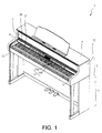
- FIG. 1 is a perspective diagram of an electronic keyboard instrument 1 to which a power control device according to an embodiment of the invention is applied.
- the electronic keyboard instrument 1 includes an instrument main body 2 and a leg portion 3 supporting the instrument main body 2.
- the left-right direction of the electronic keyboard instrument 1 is defined based on a direction in which a player looks at the keyboard instrument 1, and the front-back direction is defined by taking the player side of the keyboard instrument 1 as the "front.”
- the instrument main body 2 mainly includes a shelf 4 (see FIGs. 2A and 2B ) supported by the leg portion 3, a side board 5 disposed upright on both sides of the shelf 4, a top board 6 disposed between the side boards 5, a front board 7 suspended on the front side of the top board 6, a back board 8 (see FIGs. 2A and 2B ) suspended on the back side of the top board 6, and a keyboard lid 9 arranged below the front board 7.
- the keyboard lid 9 in a closed state is arranged across the left and right side boards 5 in a substantially horizontal manner, thereby covering a keyboard 10 that includes white keys 10a and black keys 10b, and so on.
- the keyboard lid 9 can be accommodated in an internal space 30 (see FIGs. 2A and 2B ) of the instrument main body 2 by being slid toward the front board 7. Accordingly, the keyboard lid 9 in the closed state can be opened.
- the keyboard lid 9 is equivalent to a lid of the invention.
- the electronic keyboard instrument 1 in FIG. 1 shows when the keyboard lid 9 is in an open state.
- the keyboard lid 9 in the open state exposes the keyboard 10, a wooden clapper 11 provided on both left and right sides of the keyboard 10, and an operation panel 25.
- a user can give a performance using the keyboard 10 exposed by opening the keyboard lid 9.
- a manipulator 23 (see FIG. 3 ) or an indicator 24 (see FIG. 3 ) is provided on the operation panel 25, a manipulator 23 (see FIG. 3 ) or an indicator 24 (see FIG. 3 ) is provided.
- the manipulator 23 includes a knob, or a slider, or a button or the like by which the user inputs various instructions.
- the indicator 24 is for indicating various information and is, e.g., a liquid crystal display (LCD).
- the user while checking the content indicated by the indicator 24, properly operates the manipulator 23, and can thereby perform user setting (e.g., timbre information) or status setting (e.g., volume setting) of the electronic keyboard instrument 1 or the like if necessary.
- user setting e.g., timbre information
- status setting e.g., volume setting
- a push switch (hereinafter "PUSH_SW”) 21 for turning on or off electricity supply to a main control unit 42 (see FIG. 3 ) is provided on the operation panel 25 .
- the PUSH_SW 21 is equivalent to a second switch of the invention.
- the operation panel 25 is exposed by opening the keyboard lid 9.
- the PUSH_SW 21 is a switch that can be operated in the open state of the keyboard lid 9.
- the PUSH_SW 21 is configured as an unlatch type switch.
- FIGs. 2A and 2B show an internal configuration of the instrument main body 2. Moreover, FIGs. 2A and 2B show a state of the internal configuration in the vicinity of the left side board 5 as viewed from the right side. More specifically, FIG. 2A shows the internal configuration of the instrument main body 2 in the closed state of the keyboard lid 9, while FIG. 2B shows the internal configuration of the instrument main body 2 in the open state of the keyboard lid 9.
- a dropping portion 12 close to or abutting against an upper surface of a keyslip 22 so as to cover the wooden clapper 11 and a front end surface of the keyboard 10 is provided downward from a front end portion.
- a guide pin 13 is provided on both left and right sides (i.e., in the direction perpendicular to the paper surface of FIG. 2A ) of a front end of the dropping portion 12.
- a pinion 17 is rotatably attached to both left and right sides of a back end of the keyboard lid 9.
- the pinion 17 is a member that engages with a later-described rack 15.
- a front guide groove 14 and the rack 15 are provided on the inside of each of the left and right side boards 5. Both the front guide groove 14 and the rack 15 are formed along the front-back direction (the left-right direction in FIG. 2A ) of the instrument main body 2. The rack 15 is located more backward in the instrument main body 2 than the front guide groove 14.
- the front guide groove 14 is a recessed rail that guides the moving guide pin 13. Meanwhile, the rack 15 is a member that engages with the pinion 17. The rack 15 is arranged on an upper surface of an attachment member 16 fixed to each of the left and right side boards 5.
- the keyboard lid 9 By the guide pin 13 being guided along the front guide groove 14 and the pinion 17 moving on the rack 15, the keyboard lid 9 can be moved in the front-back direction.
- the keyboard lid 9 in the closed state is moved backward, the keyboard lid 9 is accommodated in the internal space 30 of the instrument main body 2. Accordingly, as shown in FIG. 2B , the keyboard lid 9 is opened.
- a lid switch (hereinafter "LID_SW”) 20 for turning on or off electricity supply to the main control unit 42 (see FIG. 3 ) is provided on the inside of the left rack 15.
- the LID_SW 20 is equivalent to a first switch of the invention.
- the LID_SW 20 is fixed to the left attachment member 16 (the attachment member 16 illustrated in FIGs. 2A and 2B ).
- the LID_SW 20 is configured as an unlatch type switch.
- the LID_SW 20 may not only be provided on the left side but may be provided on the right side, and may also be provided on both left and right sides.
- a shaft portion 18 is inserted into the left and right pinions 17.
- An actuator 19 that operates the LID_SW 20 when the keyboard lid 9 is closed is provided on the side of the right pinion 17 on the shaft portion 18.
- the actuator 19 presses a lever portion of the LID_SW 20 and thereby operates the LID_SW 20.
- the lever portion of the LID_SW 20 remains pressed by the actuator 19.
- the LID_SW 20 is configured as an unlatch type switch, and while the keyboard lid 9 is open, the LID_SW 20 maintains a state of being operated by a mechanism of the keyboard lid 9.
- the LID_SW 20 is operated, and thereby the electricity supply to the main control unit 42 (see FIG. 3 ) including a CPU 51 and so on can be turned on or off.
- turning on electricity supply to the main control unit 42 is referred to as “turning on power”
- turning off the electricity supply is referred to as “turning off the power.”
- the electronic keyboard instrument 1 has an automatic power-off function.
- the electronic keyboard instrument 1 of the present embodiment when the power is turned off by actuation of the automatic power-off function while the keyboard lid 9 is open, without performing a closing operation of the keyboard lid 9, the power can be turned on again by operation of the PUSH_SW 21. The details thereof are described later. Due to such configuration, the function of turning on/off the power in conjunction with opening and closing of the keyboard lid 9 can suitably coexist with the automatic power-off function.
- FIG. 3 is a block diagram showing an electric configuration of the electronic keyboard instrument 1.
- the electronic keyboard instrument 1 includes a power control unit 41 and the main control unit 42.
- a power plug 71 By connecting a power plug 71 to a commercial power source (not illustrated), AC current supplied from the commercial power source is converted to DC current by an AC adapter 72 and inputted to the electronic keyboard instrument 1.
- the main control unit 42 is operated by the DC current inputted from the AC adapter 72.
- the power control unit 41 is a circuit that controls whether or not to apply the DC current inputted from the AC adapter 72 to the main control unit 42 (i.e., on/off of the power).
- the main control unit 42 is a circuit that realizes main functions such as a musical sound control function of the electronic keyboard instrument 1.
- the main control unit 42 is equivalent to a main control unit of the invention.
- the main control unit 42 includes the CPU 51, a ROM 52, a RAM 53, a flash memory 54, a sound source 55, and an input/output port (hereinafter "I/O") 56.
- the elements 51 to 56 are connected to one another through a bus line 57.
- the bus line 57 is connected to the keyboard 10, the LID_SW 20, the PUSH_SW 21, the manipulator 23 and the indicator 24.
- the electronic keyboard instrument 1 also includes a digital-to-analog converter (DAC) 58.
- the DAC 58 is connected to the sound source 55 and also to an amplifier 61 provided outside the electronic keyboard instrument 1.
- the CPU 51 is a central control unit that controls each portion of the electronic keyboard instrument 1 in accordance with fixed value data or control programs stored in the ROM 52 or the RAM 23.
- the ROM 52 is an unrewritable non-volatile memory.
- the ROM 52 stores a control program executed by the CPU 51, or the fixed value data (not illustrated) referred by the CPU 51 when the control program is executed, etc.
- the CPU 51 is equivalent to a control processor of the invention.
- the CPU 51 when no operation has been performed on the electronic keyboard instrument 1 over a certain period, the CPU 51 outputs a signal for actuating the automatic power-off function. The details thereof are described later. Therefore, the CPU 51 is equivalent to a third switch of the invention.
- the RAM 53 is a rewritable volatile memory.
- the RAM 53 is equivalent to a volatile memory of the invention. Therefore, stored content in the RAM 53 is erased when the power is turned off.
- the RAM 53 temporarily stores various data upon execution of the control program by the CPU 51.
- the user setting or the status setting by operating the manipulator 23 the user setting or the status setting copied to the RAM 53 is rewritten as a setting value after the change.
- the flash memory 54 is a rewritable non-volatile memory.
- the flash memory 54 is equivalent to a non-volatile memory of the invention. Therefore, stored content in the flash memory 54 is not erased even if the power is turned off.
- the flash memory 54 stores non-volatile memory such as the user setting or the status setting and so on.
- non-volatile memory such as the user setting or the status setting and so on.
- the sound source 55 is configured as a sampling sound source having a built-in waveform memory (not illustrated) that stores a sound source waveform.
- the sound source 55 reads, from the waveform memory, waveform data corresponding to a sound production instruction that corresponds to the pressed key 10a or 10b and that is supplied from the CPU 51, and generates a musical sound corresponding to the read waveform data and the user setting such as timbre information.
- the musical sound generated by the sound source 55 is supplied to the DAC 58 to be converted to an analog signal, amplified by the amplifier 61, and emitted from a speaker 62.
- the sound source 55 stops the musical sound being generated. Accordingly, the musical sound that was being emitted from the speaker 62 is muffled.
- the I/O 56 is connected to the power control unit 41. By input of the DC current supplied from the power control unit 41 to the main control unit 42 through the I/O 56, the elements such as the CPU 51 and so on that constitute the main control unit 42 operate.
- the power control unit 41 is connected to the LID SW 20 and the PUSH_SW 21.
- the power control unit 41 controls the on/off of the power (i.e., the on/off of the electricity supply to the main control unit 42) in response to output from the switches 20 and 21.
- the power control unit 41 turns off the power in response to output from the CPU 51.
- FIGs. 4 to 11 are block diagrams for explaining power control performed by the power control unit 41. Moreover, in FIGs. 4 to 11 , the I/O 56 interposed between the power control unit 41 and the CPU 51 is omitted from description.
- the power control unit 41 includes a logic inversion circuit 81, a LID_SW nullifying circuit 82, a determination circuit 83, a latch circuit 84, a FET_SW control circuit 85, a FET_SW 86, and a step-down circuit 87.
- These circuits 81 to 86 are operated by a +24 V adapter voltage (ADP +24 V) applied by the AC adapter 72.
- the logic inversion circuit 81 is a circuit that inverts and outputs a state of a signal supplied from the LID_SW 20. That is, when the signal supplied from the LID_SW 20 is in a HIGH state, the logic inversion circuit 81 inverts the signal to a LOW state and outputs the same. On the other hand, when the signal supplied from the LID_SW 20 is in the LOW state, the logic inversion circuit 81 inverts the signal to the HIGH state and outputs the same.
- the LID_SW 20 when the keyboard lid 9 is closed (i.e., when the LID_SW 20 is not being operated), the LID_SW 20 outputs a HIGH signal.
- the keyboard lid 9 when the keyboard lid 9 is open (i.e., when the LID_SW 20 maintains the state of being operated by the actuator 19), the LID_SW 20 outputs a LOW signal. Consequently, when the keyboard lid 9 is closed, the logic inversion circuit 81 outputs a LOW signal; when the keyboard lid 9 is open, the logic inversion circuit 81 outputs a HIGH signal.
- the signal outputted from the logic inversion circuit 81 is supplied to the LID_SW nullifying circuit 82 and the determination circuit 83 respectively.
- the LID_SW nullifying circuit 82 is a circuit that temporarily nullifies, according to a signal supplied from the CPU 51, the signal supplied from the logic inversion circuit 81 in response to the closing of the keyboard lid 9.
- the LID_SW nullifying circuit 82 is equivalent to a first nullifying circuit of the invention.
- the LID_SW nullifying circuit 82 is configured as an OR circuit. Consequently, when any of the signal supplied from the logic inversion circuit 81 and the signal supplied from the CPU 51 is a HIGH signal, the LID_SW nullifying circuit 82 outputs a HIGH signal. On the other hand, when both the signal supplied from the logic inversion circuit 81 and the signal supplied from the CPU 51 are LOW signals, the LID_SW nullifying circuit 82 outputs a LOW signal.
- both the signal supplied from the logic inversion circuit 81 and the signal supplied from the CPU 51 will be LOW signals. Therefore, when the keyboard lid 9 is closed to turn off the power, the LID_SW nullifying circuit 82 outputs a LOW signal. On the other hand, in other cases, i.e., when the keyboard lid 9 is opened to turn on the power or while the keyboard lid 9 is open, the LID_SW nullifying circuit 82 outputs a HIGH signal. The signal outputted from the LID_SW nullifying circuit 82 is supplied to the FET_SW control circuit 85.
- the LID_SW nullifying circuit 82 When the keyboard lid 9 is closed, while the LID_SW nullifying circuit 82 outputs a LOW signal, the CPU 51, after outputting a HIGH signal over a predetermined data storage period, switches to LOW. The details thereof are described later. Consequently, after the keyboard lid 9 has been closed, the LID_SW nullifying circuit 82 nullifies the LOW signal outputted from the logic inversion circuit 81 by outputting a HIGH signal over the data storage period. Accordingly, the power-off based on the closing of the keyboard lid 9 can be delayed as long as the data storage period.
- the determination circuit 83 is a circuit that outputs a signal supplied from the PUSH_SW 21 in response to the state of the keyboard lid 9.
- the determination circuit 83 is equivalent to a second nullifying circuit of the invention.
- the determination circuit 83 When the keyboard lid 9 is open, the determination circuit 83 outputs a signal in the same state as the signal supplied from the PUSH_SW 21.
- the determination circuit 83 nullifies the signal supplied from the PUSH_SW 21 in response to operation of the PUSH_SW 21.
- the PUSH_SW 21 outputs a HIGH signal when not being operated.
- the PUSH_SW 21 outputs a LOW signal when the PUSH_SW 21 is operated. Consequently, in the open state of the keyboard lid 9, when the PUSH_SW 21 is not being operated, the determination circuit 83 outputs a HIGH signal similar to that supplied from the PUSH_SW 21. On the other hand, in the open state of the keyboard lid 9, when the PUSH_SW 21 is operated, the determination circuit 83 outputs a LOW signal similar to that supplied from the PUSH_ SW 21.
- the determination circuit 83 nullifies the LOW signal supplied from the PUSH_SW 21 and outputs a HIGH signal. In this way, in the closed state of the keyboard lid 9, a signal output corresponding to operation of the PUSH_SW 21 is nullified. Thus, even if the PUSH_SW 21 is unintentionally operated in the closed state of the keyboard lid 9 (including a state in which the keyboard lid 9 is opened to an extent without operating the LID_SW 20), such situation can be ignored.
- the determination circuit 83 outputs a HIGH signal similar to that supplied from the PUSH_SW 21.
- the signal outputted from the determination circuit 83 is supplied to the latch circuit 84.
- the latch circuit 84 is a circuit that latches a state in which the power is turned on/off by operation of the PUSH_SW 21 or actuation of the automatic power-off function.
- the latch circuit 84 is equivalent to a latch circuit of the invention.
- the latch circuit 84 switches a signal that has been latched to the LOW state to the HIGH state. Accordingly, the latch circuit 84 outputs a HIGH signal.
- the latch circuit 84 switches a signal that has been latched to the HIGH state to the LOW state. Accordingly, the latch circuit 84 outputs a LOW signal.
- the latch circuit 84 holds a LOW signal.
- the CPU 51 When the PUSH_SW 21 is operated in order to turn off the power during operation of the CPU 51, the CPU 51, after outputting a LOW signal over the predetermined data storage period, switches the signal to the HIGH state. The details thereof are described later.
- the CPU 51 when the automatic power-off function is actuated due to no operation being performed over a certain time during operation of the CPU 51, similarly to when the PUSH_SW 21 is operated, the CPU 51, after outputting a LOW signal over the predetermined data storage period, switches the signal to the HIGH state.
- the latch circuit 84 latches and outputs a LOW signal during a period from when the PUSH_SW 21 is operated or when the automatic power-off function is actuated until when the data storage period passes. Then, after the data storage period has passed, the latch circuit 84 latches and outputs a HIGH signal.
- the signal outputted from the latch circuit 84 is supplied to the FET_SW control circuit 85.
- the FET_SW control circuit 85 controls the power to be off. The details thereof are described later.
- the determination circuit 83 outputs a LOW signal. Consequently, in response to the fact that a LOW signal is supplied from the determination circuit 83 when the power is off, the latch circuit 84 switches a signal that has been latched to the HIGH state to the LOW state. In this case, the FET_SW control circuit 85 controls the power to be off by switching the signal outputted from the latch circuit 84 to the LOW state. The details thereof are described later.
- the FET_SW control circuit 85 is a circuit that controls a FET switch (hereinafter "FET_SW") 86 based on a signal supplied from the LID_SW nullifying circuit 82 and a signal supplied from the latch circuit 84.
- FET_SW a FET switch
- the FET_SW control circuit 85 is equivalent to a power control circuit of the invention.
- FET is an abbreviation of field-effect transistor.
- the FET_SW control circuit 85 When the signal supplied from the latch circuit 84 is a LOW signal and the signal supplied from the LID_SW nullifying circuit 82 is a HIGH signal, the FET_SW control circuit 85 outputs a LOW signal. When the output from the FET_SW control circuit 85 is in the LOW state, the FET_SW 86 is turned on. As a result, a 3.3 V system voltage (P +3.3 V) stepped-down from a +24 V internal voltage (P +24 V) by the step-down circuit 87 is outputted.
- the system voltage is a voltage for causing the main control unit 42 to operate. That is, by output of the system voltage from the step-down circuit 87, the power is turned on.
- the FET_SW control circuit 85 When the signal supplied from the LID_SW nullifying circuit 82 is a LOW signal, the FET_SW control circuit 85 also outputs a HIGH signal. When the output from the FET_SW control circuit 85 is in the HIGH state, the FET_SW 86 is turned off. As a result, the system voltage for causing the main control unit 42 to operate is not outputted. In other words, the power is turned off.
- the situation in which the signal supplied from the latch circuit 84 is a HIGH signal is that a HIGH signal is outputted from the CPU 51 due to passage of the data storage period after the PUSH_SW 21 is operated or after the automatic power-off function is actuated.
- the situation in which the signal supplied from the LID_SW nullifying circuit 82 is a LOW signal is that the keyboard lid 9 is closed. Therefore, in these situations, the power is turned off.
- FIG. 4 is a block diagram of a case where the power is turned on by opening of the keyboard lid 9. Moreover, in FIGs. 4 to 11 , an arrow in thick solid line indicates a HIGH signal. On the other hand, an arrow in thin solid line indicates a LOW signal.
- the LID_SW 20 in response to the opening of the keyboard lid 9, the LID_SW 20 outputs a LOW signal. Accordingly, the logic inversion circuit 81 outputs a HIGH signal. Since the power is off, the CPU 51 does not operate. Consequently, the LID_SW nullifying circuit 82 outputs a HIGH signal.
- the PUSH_SW 21 since the PUSH_SW 21 is not being operated, the PUSH_SW 21 outputs a HIGH signal. As described above, since the logic inversion circuit 81 outputs a HIGH signal, the determination circuit 83 outputs a HIGH signal. Since the CPU 51 does not operate, the latch circuit 84 outputs a LOW signal due to the supply of the HIGH signal from the determination circuit 83.
- the FET_SW control circuit 85 since the FET_SW control circuit 85 is supplied with a LOW signal from the latch circuit 84 and a HIGH signal from the LID_SW nullifying circuit 82, the FET_SW control circuit 85 outputs a LOW signal. Accordingly, the FET_SW 86 is turned on, and the system voltage is outputted from the step-down circuit 87. That is, the power is turned on, so that the main control unit 42 operates.
- FIGs. 5 and 6 are block diagrams of cases where the power is turned off by actuation of the automatic power-off function while the keyboard lid 9 is open. More specifically, FIG. 5 illustrates the case during the data storage period, and FIG. 6 illustrates the case after the data storage period has passed.
- the LID_SW 20 outputs a LOW signal. Consequently, the logic inversion circuit 81 outputs a HIGH signal.
- the CPU 51 outputs a LOW signal to the LID_SW nullifying circuit 82. Consequently, the LID_SW nullifying circuit 82 outputs a HIGH signal.
- the PUSH_SW 21 since the PUSH_SW 21 is not being operated, the PUSH_SW 21 outputs a HIGH signal. Accordingly, the determination circuit 83 outputs a HIGH signal. After the automatic power-off function is actuated and during the data storage period, the CPU 51 outputs a LOW signal to the latch circuit 84. Consequently, the latch circuit 84 outputs a LOW signal.
- the FET_SW control circuit 85 is supplied with a LOW signal from the latch circuit 84 and a HIGH signal from the LID_SW nullifying circuit 82, the FET_SW control circuit 85 outputs a LOW signal. Accordingly, the FET_SW 86 is turned on. Consequently, since the system voltage is continuously outputted from the step-down circuit 87, the main control unit 42 continues to operate.
- the CPU 51 When the data storage period passes, as shown in FIG. 6 , the CPU 51 outputs a HIGH signal to the latch circuit 84. Consequently, the latch circuit 84 outputs a HIGH signal. As a result, the FET_SW control circuit 85 outputs a HIGH signal. Accordingly, the FET_SW 86 is turned off, and the power is turned off.
- FIG. 7 is a block diagram of a case where the power is turned on by operation of the PUSH_SW 21. Since the PUSH_SW 21 is a switch that can be operated in the open state of the keyboard lid 9, in such case, the keyboard lid 9 is open. Consequently, as shown in FIG. 7 , the LID_SW 20 outputs a LOW signal. Accordingly, the logic inversion circuit 81 outputs a HIGH signal. Since the power is off, the CPU 51 does not operate. Consequently, the LID_SW nullifying circuit 82 outputs a HIGH signal due to the supply of the HIGH signal from the logic inversion circuit 81.
- the PUSH_SW 21 since the PUSH_SW 21 is operated, the PUSH_SW 21 outputs a LOW signal. As described above, since the logic inversion circuit 81 outputs a HIGH signal, the determination circuit 83 outputs a LOW signal. Since the CPU 51 does not operate, the latch circuit 84 outputs a LOW signal due to the supply of the LOW signal from the determination circuit 83.
- the FET_SW control circuit 85 since the FET_SW control circuit 85 is supplied with a LOW signal from the latch circuit 84 and a HIGH signal from the LID_SW nullifying circuit 82, the FET_SW control circuit 85 outputs a LOW signal. Accordingly, the FET_SW 86 is turned on, and the power is turned on, so that the main control unit 42 operates.
- FIGs. 8 and 9 are block diagrams of cases where the power is turned off by closing of the keyboard lid 9. More specifically, FIG. 8 illustrates the case during the data storage period, and FIG. 9 illustrates the case after the data storage period has passed.
- the LID_SW 20 in response to the closing of the keyboard lid 9, the LID_SW 20 outputs a HIGH signal. Accordingly, the logic inversion circuit 81 outputs a LOW signal. After the keyboard lid 9 has been closed and during the data storage period, the CPU 51 outputs a HIGH signal to the LID_SW nullifying circuit 82. Consequently, the LID_SW nullifying circuit 82 outputs a HIGH signal.
- the PUSH_SW 21 since the PUSH_SW 21 is not being operated, the PUSH_SW 21 outputs a HIGH signal. Accordingly, the determination circuit 83 outputs a LOW signal. The CPU 51 outputs a LOW signal to the latch circuit 84. Consequently, the latch circuit 84 outputs a LOW signal.
- the FET_SW control circuit 85 is supplied with a LOW signal from the latch circuit 84 and a HIGH signal from the LID_SW nullifying circuit 82, the FET_SW control circuit 85 outputs a LOW signal. Accordingly, the FET_SW 86 is turned on. Consequently, since the system voltage is continuously outputted from the step-down circuit 87, the main control unit 42 continues to operate.
- the CPU 51 When the data storage period passes, as shown in FIG. 9 , the CPU 51 outputs a LOW signal to the LID_SW nullifying circuit 82. Consequently, the LID_SW nullifying circuit 82 outputs a LOW signal. Accordingly, the FET_SW control circuit 85 outputs a HIGH signal. Accordingly, the FET_SW 86 is turned off, and the power is turned off.
- FIGs. 10 and 11 are block diagrams of cases where the power is turned off by operation of the PUSH_SW 21. More specifically, FIG. 10 illustrates the case during the data storage period, and FIG. 11 illustrates the case after the data storage period has passed.
- the LID_SW 20 outputs a LOW signal. Consequently, the logic inversion circuit 81 outputs a HIGH signal.
- the CPU 51 outputs a LOW signal to the LID_SW nullifying circuit 82. Consequently, the LID_SW nullifying circuit 82 outputs a HIGH signal.
- the PUSH_SW 21 since the PUSH_SW 21 is operated, the PUSH_SW 21 outputs a LOW signal. Accordingly, the determination circuit 83 outputs a LOW signal. After the PUSH_SW 21 is operated and during the data storage period, the CPU 51 outputs a LOW signal to the latch circuit 84. Consequently, the latch circuit 84 outputs a LOW signal.
- the FET_SW control circuit 85 is supplied with a LOW signal from the latch circuit 84 and a HIGH signal from the LID_SW nullifying circuit 82, the FET_SW control circuit 85 outputs a LOW signal. Accordingly, the FET_SW 86 is turned on. Consequently, since the system voltage is continuously outputted from the step-down circuit 87, the main control unit 42 continues to operate.
- the CPU 51 When the data storage period passes, as shown in FIG. 11 , the CPU 51 outputs a HIGH signal to the latch circuit 84. Consequently, the latch circuit 84 outputs a HIGH signal. As a result, the FET_SW control circuit 85 outputs a HIGH signal. Accordingly, the FET_SW 86 is turned off, and the power is turned off.
- FIG. 12 is a flowchart showing a power control process executed by the CPU 51 of the electronic keyboard instrument 1.
- This process is a process that controls the state of the signals outputted by the CPU 51 to the LID_SW nullifying circuit 82 and to the latch circuit 84 respectively when the power is on. This process is started in response to turn-on of the power and supply of electricity to the CPU 51, and the CPU 51 executes this process while the power is on.
- the CPU 51 outputs a HIGH signal to the LID_SW nullifying circuit 82, and outputs a LOW signal to the latch circuit 84 (S1).
- the CPU 51 determines whether a HIGH signal is received from the LID_SW 20 (S2). If determining that a HIGH signal is received from the LID_SW 20 (S2: Yes), the CPU 51 moves to the process in S4.
- the CPU 51 determines whether a LOW signal is received from the PUSH_SW 21 (S10). If determining that a LOW signal is received from the PUSH_SW 21 (S10: Yes), the CPU 51 moves to the process in S4.
- the CPU 51 If determining that no LOW signal is received from the PUSH_SW 21 (S10: No), the CPU 51 starts the time counting of a period (hereinafter "standby period") during which actuation of the automatic power-off function is awaited (S11) and then determines whether any operation has been performed (S12). If determining that an operation has been performed (S12: Yes), the CPU 51 clears the standby period (S14), and moves the process to S2. On the other hand, if determining that no operation has been performed (S12: No), the CPU 51 determines whether the standby period has passed (S13).
- standby period a period during which actuation of the automatic power-off function is awaited
- the CPU 51 stores, in the flash memory 54, the stored content in the RAM 53 (S4), and waits until such storage is completed (S5: No). That is, the power remains on until the storage is completed.
- the CPU 51 determines whether a LID (keyboard lid 9) is closed, i.e., whether a HIGH signal is received from the LID_SW 20 (S6). If determining that the LID (keyboard lid 9) is closed, i.e., that a HIGH signal is received from the LID_SW 20 (S6: Yes), the CPU 51 outputs a LOW signal to the LID_SW nullifying circuit 82 (S7) to turn off the power (S9), so as to end this process.
- the CPU 51 outputs a HIGH signal to the latch circuit 84 (S8) to turn off the power (S9), so as to end this process.
- the process in S5 executed by the CPU 51 is equivalent to a delay process of the invention.
- the process in S1 executed by the CPU 51 is equivalent to a first output process of the invention.
- the process in S8 executed by the CPU 51 is equivalent to a second output process of the invention.
- the FET_SW control circuit 85 when the automatic power-off function is actuated while the keyboard lid 9 is open, the FET_SW control circuit 85 turns off the power (i.e., turns off the electricity supply to the main control unit 42) based on a HIGH signal outputted from the latch circuit 84. On the other hand, when a LOW signal is outputted from the latch circuit 84 in the case where the power is off, the FET_SW control circuit 85 turns on the power based on the LOW signal.
- the signal of the latch circuit 84 can be inverted to the LOW state.
- the power can be turned on. Since the power can be turned on again without temporarily closing the open keyboard lid 9, the electronic keyboard instrument 1 can be activated in a smart manner. In this way, the function of turning on/off the power in conjunction with opening and closing of the keyboard lid 9 can suitably coexist with the automatic power-off function.
- the CPU 51 does not operate during the standby period while the electronic keyboard instrument 1 is not being operated, and electricity (standby electricity) consumed during the standby period can be reduced.
- the power control unit 41 that is actuated with lower standby electricity.
- the configuration in which operation of the LID_SW 20 or operation of the PUSH_SW 21 is detected by the power control unit 41 has the following problem. Because the operation of the LID_SW 20 or the operation of the PUSH_SW 21 according to closing of the keyboard lid 9 performed when the power is on is immediately detected by the power control unit 41, and the power is immediately turned off, the content that was stored in the RAM 53, such as timbre information or the like, is lost.
- the CPU 51 delays output of a signal for turning off the power until the data storage period passes, and thus loss of the stored content in the RAM 53 can be prevented.
- the data storage period is not necessarily 5 seconds, but may have a suitable length.
- the standby period is not necessarily 10 minutes, but may have a suitable length.
- the data storage period and the standby period may have a variable length set by the user.
- an electronic musical instrument equipped with the power control device of the invention is exemplified by the electronic keyboard instrument 1 having a configuration in which the power can be turned on/off in response to opening and closing of the keyboard lid 9.
- the invention is applicable not only to a keyboard instrument like the electronic keyboard instrument 1, but also to any electronic musical instrument having a configuration in which the power can be turned on/off in response to opening and closing of a lid.
- a synthesizer provided with a lid that covers an operation panel has a configuration in which the power can be turned on/off in response to opening and closing of the lid
- the invention is also applicable to the synthesizer.
- the stored content in the RAM 53 is stored in the flash memory 54.
- such storage may not be performed.
- the process of the CPU 51 inverting the state of an output signal during or after the data storage period, i.e., the processes in S7 and S8, is no longer needed.
- the LID_SW nullifying circuit 82 is also no longer needed.
- a destination to store the stored content in the RAM 53 is exemplified by the flash memory 54 that is built in the electronic keyboard instrument 1.
- the destination may be various non-volatile memories (e.g., a USB-connected flash memory or hard disk, etc.) detachably connected to the electronic keyboard instrument 1.
- the determination circuit 83 is provided to which a signal outputted from the PUSH_SW 21 and a signal outputted from the logic inversion circuit 81 are supplied.
- the determination circuit 83 may not be provided, and the signal outputted from the PUSH_SW 21 and the signal outputted from the logic inversion circuit 81 may be supplied to the latch circuit 84.
- the LID_SW 20 is provided inside the instrument main body 2.
- the actuator 19 operates the LID_SW 20; when the keyboard lid 9 is closed, the actuator 19 separates from the LID_SW 20 to cancel the operation.
- the LID_SW 20 can be disposed in various positions.
- the LID_SW 20 can be provided on the wooden clapper 11.
- the keyboard lid is of a type that rotates about a rotating shaft.
- the PUSH_SW 21 is an unlatch type switch.
- the PUSH_SW 21 can also be a latch type switch.
- the PUSH_SW 21 is a latch type switch, after the power is turned off by the automatic power-off function, it will be necessary to operate the PUSH_SW 21 once to return it to the off state and then operate it to turn it on again.
- the electronic keyboard instrument 1 can be activated in a smart manner.
- the PUSH_SW 21 is provided in a position exposed by opening the keyboard lid 9.
- the PUSH_SW 21 may be provided in a position that is exposed regardless of opening and closing of the keyboard lid 9.
- there may be a foot switch or the like connected to the electronic keyboard instrument 1 by a cable.
- the switches such as the LID_SW 20 or the circuits such as the LID_SW nullifying circuit 82 output a HIGH signal or a LOW signal in each situation have been explained.
- the invention is not limited thereto. That is, the switches or the circuits may be configured to output signals opposite to those explained in the above embodiments. Namely, in the case mentioned above where a HIGH signal is outputted, a LOW signal may be outputted, and in the case mentioned above where a LOW signal is outputted, a HIGH signal may be outputted. With such configuration, the same effects as the above embodiments can still be obtained.
Abstract
Description
- The invention relates to a power control device of an electronic musical instrument, particularly to a power control device that allows a function of turning on/off power in conjunction with opening and closing of a lid of an electronic musical instrument to suitably coexist with a function of automatically turning off the power when no operation is performed over a predetermined period.
-
Patent Literature 1 describes an electronic keyboard instrument whose power is switched between on and off in response to opening and closing of a lid (hereinafter "keyboard lid") that covers a keyboard. - [Patent Literature 1] Japanese Patent No.
4962148 - In
Patent Literature 1, the function (hereinafter "automatic power-off function") of automatically turning off the power when no operation is performed over a certain period is not taken into account. If the automatic power-off function is loaded into the electronic musical instrument whose power is turned on/off by opening and closing of the keyboard lid, when the automatic power-off function causes a power-off while the keyboard lid is open, to turn on the power again, it will be necessary to close the open keyboard lid temporarily and then open it again. However, performing the closing operation of the keyboard lid takes time and is not smart. - The invention has been made in view of the aforementioned matters and provides a power control device that allows a function of turning on/off power in conjunction with opening and closing of a lid of an electronic musical instrument to suitably coexist with the automatic power-off function.
- In order to achieve the above purpose, according to the power control device of a technical solution of the invention, when electricity supply to a main control unit including an electricity-operated control processor is off, a power control circuit turns on the electricity supply to the main control unit based on a signal outputted from a first switch in response to opening of the lid. In the case where the electricity supply to the main control unit is on, when the electricity supply to the main control unit is turned off based on a signal outputted from a third switch in response to no operation being performed over a predetermined time, a latch circuit holds a first state signal for turning off the electricity supply to the main control unit. On the other hand, when a signal for turning on the electricity supply to the main control unit is outputted from a second switch due to operation of the second switch, the latch circuit holds, in place of the first state signal, a second state signal for turning on the electricity supply to the main control unit.
- When the first state signal is outputted from the latch circuit while the lid is open, the power control circuit turns off the electricity supply to the main control unit based on the first state signal. On the other hand, when the second state signal is outputted from the latch circuit in the case where the electricity supply to the main control unit is off, the power control circuit turns on the electricity supply to the main control unit based on the second state signal.
- Therefore, while the lid is open, even after the electricity supply to the main control unit is turned off in response to no operation being performed over the predetermined time, by operation of the second switch, the second state signal is outputted from the latch circuit. Thus, the electricity supply to the main control unit can be turned on without temporarily closing the open lid. Accordingly, the function of turning on/off the power in conjunction with opening and closing of the lid of the electronic musical instrument can suitably coexist with the automatic power-off function.
- According to the power control device of a second technical solution, in addition to the effects accomplished by the aforementioned technical solution, the following effects are achieved. When the signal for turning off the electricity supply to the main control unit is outputted from the first switch or the second switch in response to the closing of the lid or the operation of the second switch while the electricity supply to the main control unit is on, the control processor executes a delay process that delays output of the signal for turning off the electricity supply to the main control unit as long as a period for storing, in a non-volatile memory contained in the main control unit, content of a volatile memory contained in the main control unit. Then, in response to output of the signal for turning off the electricity supply to the main control unit from the control processor, the power control circuit turns off the electricity supply to the main control unit. Therefore, it can be prevented that the electricity supply to the main control unit is immediately turned off in response to a signal output from the first switch or the second switch and that the content stored in the volatile memory is lost.
- According to the power control device of a third technical solution, in addition to the effects accomplished by the aforementioned technical solutions, the following effects are achieved. During the execution of the delay process, the control processor executes a first output process outputting a signal that nullifies the turn-off of the electricity supply to the main control unit. Over a period while the signal is being outputted by the first output process, a first nullifying circuit nullifies the signal that is for turning off the electricity supply to the main control unit and that is outputted from the first switch in response to the closing of the lid. Therefore, a period from when the lid is closed until when the electricity supply to the main control unit is turned off can be delayed by a period of time delayed. Accordingly, it can be prevented that the electricity supply to the main control unit is immediately turned off in response to the signal output from the first switch and that the content stored in the volatile memory is lost.
- According to the power control device of a fourth technical solution, in addition to the effects accomplished by the aforementioned technical solutions, the following effects are achieved. When the signal for turning off the electricity supply to the main control unit is outputted from the second switch in response to the operation of the second switch while the electricity supply to the main control unit is on, the control processor, after executing the delay process, executes a second output process outputting the signal for turning off the electricity supply to the main control unit to the latch circuit. Therefore, a period from when the second switch is operated until when the first state signal is outputted from the latch circuit to turn off the electricity supply to the main control unit can be delayed by a period of time delayed. Accordingly, it can be prevented that the electricity supply to the main control unit is immediately turned off in response to the signal output from the second switch and that the content stored in the volatile memory is lost.
- According to the power control device of a fifth technical solution, in addition to the effects accomplished by the aforementioned technical solutions, the following effects are achieved. The second switch is a switch covered by the lid in a closed state of the lid and exposed in an open state of the lid. When the lid is closed, a second nullifying circuit nullifies the signal outputted from the second switch due to the operation of the second switch. Therefore, even if the second switch is unintentionally operated in the closed state of the lid, turn-on of the electricity supply to the main control unit thereby caused can be prevented.
- According to the power control device of a sixth technical solution, when the lid is open, the second nullifying circuit outputs a signal having the same level as that of the signal supplied from the second switch.
- According to the power control device of a seventh technical solution, the first nullifying circuit outputs, to the power control circuit, a signal corresponding to a level of the signal supplied from the first switch or the control processor, and the power control circuit turns on or off the electricity supply to the main control unit based on the signal outputted from the latch circuit and the signal outputted from the first nullifying circuit.
- According to the power control device of an eighth technical solution, when the signal outputted from the latch circuit has a second level and the signal outputted from the first nullifying circuit has a first level, the power control circuit turns on the electricity supply to the main control unit.
- According to the power control device of a ninth technical solution, when the electricity supply to the main control unit is turned off based on the signal outputted from the third switch, or when the lid is opened, the power is on and the second switch is operated, the power control circuit changes the signal to be outputted from the latch circuit from the second level to the first level so as to turn off the electricity supply to the main control unit.
- According to the power control device of a tenth technical solution, when the power is turned off by the closing of the lid, the power control circuit changes the signal to be outputted from the first nullifying circuit from the first level to the second level so as to turn off the electricity supply to the main control unit.
- According to the power control device of an eleventh technical solution, the latch circuit outputs the signal having the first level to the power control circuit when the electricity supply to the main control unit is turned off based on the signal outputted from the third switch or when the lid is opened, the power is on, and the second switch is operated, and outputs the signal having the second level to the power control circuit when the signal for turning on the electricity supply to the main control unit is outputted from the second switch due to the operation of the second switch; the first nullifying circuit outputs the signal having the first level to the power control circuit when the lid is opened to turn on the power or while the lid is open, and outputs the signal having the second level to the power control circuit when the lid is closed to turn off the power; and the power control circuit outputs the signal for turning on the electricity supply to the main control unit when the signal supplied from the latch circuit has the second level and the signal supplied from the first nullifying circuit has the first level, and outputs the signal for turning off the electricity supply to the main control unit when the signal supplied from the latch circuit has the first level or the signal supplied from the first nullifying circuit has the second level.
- According to the power control device of a twelfth technical solution, the first nullifying circuit is configured as an OR circuit.
- According to the power control device of a thirteenth technical solution, the power control device further includes a logic inversion circuit that inverts a state of the signal supplied from the first switch and supplies it to the first nullifying circuit and the second nullifying circuit respectively.
- According to the power control device of a fourteenth technical solution, in addition to the effects accomplished by the aforementioned technical solutions, the following effects are achieved. The second switch is an unlatch type switch. Thus, while the lid is open, when the electricity supply to the main control unit is turned off in response to no operation being performed over the predetermined time, there is no need to operate the second switch once to return it to the off state and then operate it to turn it on again. Therefore, the electronic musical instrument can be activated in a smart manner.
- According to the power control device of a fifteenth technical solution, in addition to the effects accomplished by the aforementioned technical solutions, the following effects are achieved. The lid is a keyboard lid that covers a keyboard when in the closed state and exposes the keyboard when in the open state. Thus, the electricity supply to the main control unit can be turned on by the act of opening the keyboard lid in order to use the keyboard. Therefore, an electronic keyboard instrument can be activated in a smart manner.
-
-
FIG. 1 is a perspective diagram of an electronic keyboard instrument to which a power control device according to an embodiment of the invention is applied. -
FIGs. 2A and 2B show an internal configuration of an instrument main body. -
FIG. 3 is a block diagram showing an electric configuration of the electronic keyboard instrument. -
FIG. 4 is a block diagram for explaining power control performed by a power control unit. -
FIG. 5 is a block diagram for explaining power control performed by the power control unit. -
FIG. 6 is a block diagram for explaining power control performed by the power control unit. -
FIG. 7 is a block diagram for explaining power control performed by the power control unit. -
FIG. 8 is a block diagram for explaining power control performed by the power control unit. -
FIG. 9 is a block diagram for explaining power control performed by the power control unit. -
FIG. 10 is a block diagram for explaining power control performed by the power control unit. -
FIG. 11 is a block diagram for explaining power control performed by the power control unit. -
FIG. 12 is a flowchart showing a power control process executed by a CPU. - Preferred embodiments of the invention are explained hereinafter with reference to the accompanying drawings.
FIG. 1 is a perspective diagram of anelectronic keyboard instrument 1 to which a power control device according to an embodiment of the invention is applied. As shown inFIG. 1 , theelectronic keyboard instrument 1 includes an instrumentmain body 2 and aleg portion 3 supporting the instrumentmain body 2. Moreover, the left-right direction of theelectronic keyboard instrument 1 is defined based on a direction in which a player looks at thekeyboard instrument 1, and the front-back direction is defined by taking the player side of thekeyboard instrument 1 as the "front." - The instrument
main body 2 mainly includes a shelf 4 (seeFIGs. 2A and 2B ) supported by theleg portion 3, aside board 5 disposed upright on both sides of theshelf 4, atop board 6 disposed between theside boards 5, afront board 7 suspended on the front side of thetop board 6, a back board 8 (seeFIGs. 2A and 2B ) suspended on the back side of thetop board 6, and a keyboard lid 9 arranged below thefront board 7. - The keyboard lid 9 in a closed state is arranged across the left and
right side boards 5 in a substantially horizontal manner, thereby covering akeyboard 10 that includeswhite keys 10a andblack keys 10b, and so on. The keyboard lid 9 can be accommodated in an internal space 30 (seeFIGs. 2A and 2B ) of the instrumentmain body 2 by being slid toward thefront board 7. Accordingly, the keyboard lid 9 in the closed state can be opened. The keyboard lid 9 is equivalent to a lid of the invention. - Moreover, the
electronic keyboard instrument 1 inFIG. 1 shows when the keyboard lid 9 is in an open state. The keyboard lid 9 in the open state exposes thekeyboard 10, awooden clapper 11 provided on both left and right sides of thekeyboard 10, and anoperation panel 25. A user can give a performance using thekeyboard 10 exposed by opening the keyboard lid 9. - On the
operation panel 25, a manipulator 23 (seeFIG. 3 ) or an indicator 24 (seeFIG. 3 ) is provided. Themanipulator 23 includes a knob, or a slider, or a button or the like by which the user inputs various instructions. Theindicator 24 is for indicating various information and is, e.g., a liquid crystal display (LCD). The user, while checking the content indicated by theindicator 24, properly operates themanipulator 23, and can thereby perform user setting (e.g., timbre information) or status setting (e.g., volume setting) of theelectronic keyboard instrument 1 or the like if necessary. - In addition, on the
operation panel 25, a push switch (hereinafter "PUSH_SW") 21 for turning on or off electricity supply to a main control unit 42 (seeFIG. 3 ) is provided. ThePUSH_SW 21 is equivalent to a second switch of the invention. As described above, theoperation panel 25 is exposed by opening the keyboard lid 9. Thus, thePUSH_SW 21 is a switch that can be operated in the open state of the keyboard lid 9. ThePUSH_SW 21 is configured as an unlatch type switch. - Next, opening and closing of the keyboard lid 9 are explained with reference to
FIGs. 2A and 2B. FIGs. 2A and 2B show an internal configuration of the instrumentmain body 2. Moreover,FIGs. 2A and 2B show a state of the internal configuration in the vicinity of theleft side board 5 as viewed from the right side. More specifically,FIG. 2A shows the internal configuration of the instrumentmain body 2 in the closed state of the keyboard lid 9, whileFIG. 2B shows the internal configuration of the instrumentmain body 2 in the open state of the keyboard lid 9. - As shown in
FIG. 2A , in the keyboard lid 9 in the closed state, a droppingportion 12 close to or abutting against an upper surface of akeyslip 22 so as to cover thewooden clapper 11 and a front end surface of thekeyboard 10 is provided downward from a front end portion. Aguide pin 13 is provided on both left and right sides (i.e., in the direction perpendicular to the paper surface ofFIG. 2A ) of a front end of the droppingportion 12. Meanwhile, apinion 17 is rotatably attached to both left and right sides of a back end of the keyboard lid 9. Thepinion 17 is a member that engages with a later-describedrack 15. - In the instrument
main body 2, afront guide groove 14 and therack 15 are provided on the inside of each of the left andright side boards 5. Both thefront guide groove 14 and therack 15 are formed along the front-back direction (the left-right direction inFIG. 2A ) of the instrumentmain body 2. Therack 15 is located more backward in the instrumentmain body 2 than thefront guide groove 14. - The
front guide groove 14 is a recessed rail that guides the movingguide pin 13. Meanwhile, therack 15 is a member that engages with thepinion 17. Therack 15 is arranged on an upper surface of anattachment member 16 fixed to each of the left andright side boards 5. - By the
guide pin 13 being guided along thefront guide groove 14 and thepinion 17 moving on therack 15, the keyboard lid 9 can be moved in the front-back direction. When the keyboard lid 9 in the closed state is moved backward, the keyboard lid 9 is accommodated in theinternal space 30 of the instrumentmain body 2. Accordingly, as shown inFIG. 2B , the keyboard lid 9 is opened. - On the inside of the
left rack 15, a lid switch (hereinafter "LID_SW") 20 for turning on or off electricity supply to the main control unit 42 (seeFIG. 3 ) is provided. TheLID_SW 20 is equivalent to a first switch of the invention. TheLID_SW 20 is fixed to the left attachment member 16 (theattachment member 16 illustrated inFIGs. 2A and 2B ). TheLID_SW 20 is configured as an unlatch type switch. Moreover, theLID_SW 20 may not only be provided on the left side but may be provided on the right side, and may also be provided on both left and right sides. - A
shaft portion 18 is inserted into the left and right pinions 17. An actuator 19 that operates theLID_SW 20 when the keyboard lid 9 is closed is provided on the side of theright pinion 17 on theshaft portion 18. When the keyboard lid 9 is open, as shown inFIG. 2B , theactuator 19 presses a lever portion of theLID_SW 20 and thereby operates theLID_SW 20. While the keyboard lid 9 is open, the lever portion of theLID_SW 20 remains pressed by theactuator 19. As described above, theLID_SW 20 is configured as an unlatch type switch, and while the keyboard lid 9 is open, theLID_SW 20 maintains a state of being operated by a mechanism of the keyboard lid 9. - In the
electronic keyboard instrument 1 of the present embodiment, by opening and closing of the keyboard lid 9, theLID_SW 20 is operated, and thereby the electricity supply to the main control unit 42 (seeFIG. 3 ) including aCPU 51 and so on can be turned on or off. Hereinafter, turning on electricity supply to themain control unit 42 is referred to as "turning on power," and turning off the electricity supply is referred to as "turning off the power." - On the other hand, the
electronic keyboard instrument 1 has an automatic power-off function. According to theelectronic keyboard instrument 1 of the present embodiment, when the power is turned off by actuation of the automatic power-off function while the keyboard lid 9 is open, without performing a closing operation of the keyboard lid 9, the power can be turned on again by operation of thePUSH_SW 21. The details thereof are described later. Due to such configuration, the function of turning on/off the power in conjunction with opening and closing of the keyboard lid 9 can suitably coexist with the automatic power-off function. -
FIG. 3 is a block diagram showing an electric configuration of theelectronic keyboard instrument 1. As shown inFIG. 3 , theelectronic keyboard instrument 1 includes apower control unit 41 and themain control unit 42. By connecting apower plug 71 to a commercial power source (not illustrated), AC current supplied from the commercial power source is converted to DC current by anAC adapter 72 and inputted to theelectronic keyboard instrument 1. Themain control unit 42 is operated by the DC current inputted from theAC adapter 72. Thepower control unit 41 is a circuit that controls whether or not to apply the DC current inputted from theAC adapter 72 to the main control unit 42 (i.e., on/off of the power). - The
main control unit 42 is a circuit that realizes main functions such as a musical sound control function of theelectronic keyboard instrument 1. Themain control unit 42 is equivalent to a main control unit of the invention. Themain control unit 42 includes theCPU 51, aROM 52, aRAM 53, aflash memory 54, asound source 55, and an input/output port (hereinafter "I/O") 56. Theelements 51 to 56 are connected to one another through abus line 57. Thebus line 57 is connected to thekeyboard 10, theLID_SW 20, thePUSH_SW 21, themanipulator 23 and theindicator 24. Theelectronic keyboard instrument 1 also includes a digital-to-analog converter (DAC) 58. TheDAC 58 is connected to thesound source 55 and also to anamplifier 61 provided outside theelectronic keyboard instrument 1. - The
CPU 51 is a central control unit that controls each portion of theelectronic keyboard instrument 1 in accordance with fixed value data or control programs stored in theROM 52 or theRAM 23. TheROM 52 is an unrewritable non-volatile memory. TheROM 52 stores a control program executed by theCPU 51, or the fixed value data (not illustrated) referred by theCPU 51 when the control program is executed, etc. TheCPU 51 is equivalent to a control processor of the invention. - In addition, when no operation has been performed on the
electronic keyboard instrument 1 over a certain period, theCPU 51 outputs a signal for actuating the automatic power-off function. The details thereof are described later. Therefore, theCPU 51 is equivalent to a third switch of the invention. - The
RAM 53 is a rewritable volatile memory. TheRAM 53 is equivalent to a volatile memory of the invention. Therefore, stored content in theRAM 53 is erased when the power is turned off. TheRAM 53 temporarily stores various data upon execution of the control program by theCPU 51. - In addition, the user setting such as timbre information or the status setting (e.g., volume setting, or brightness setting of the
indicator 24, etc.) of theelectronic keyboard instrument 1, or the like, which is stored in theflash memory 54, is copied from theflash memory 54 to theRAM 53. When the user changes the user setting or the status setting by operating themanipulator 23, the user setting or the status setting copied to theRAM 53 is rewritten as a setting value after the change.
Theflash memory 54 is a rewritable non-volatile memory. Theflash memory 54 is equivalent to a non-volatile memory of the invention. Therefore, stored content in theflash memory 54 is not erased even if the power is turned off. Theflash memory 54 stores non-volatile memory such as the user setting or the status setting and so on. When an event occurs in which the power is turned off when the keyboard lid 9 is closed or when the automatic power-off function is actuated, or the like, theelectronic keyboard instrument 1 stores, in theflash memory 54, the user setting or the status setting that has been stored in theRAM 53 before the power is turned off. The details thereof are described later. - The
sound source 55 is configured as a sampling sound source having a built-in waveform memory (not illustrated) that stores a sound source waveform. When the key 10a or 10b of thekeyboard 10 is pressed, thesound source 55 reads, from the waveform memory, waveform data corresponding to a sound production instruction that corresponds to the pressed key 10a or 10b and that is supplied from theCPU 51, and generates a musical sound corresponding to the read waveform data and the user setting such as timbre information. The musical sound generated by thesound source 55 is supplied to theDAC 58 to be converted to an analog signal, amplified by theamplifier 61, and emitted from aspeaker 62. On the other hand, when the key 10a or 10b is no longer pressed, thesound source 55 stops the musical sound being generated. Accordingly, the musical sound that was being emitted from thespeaker 62 is muffled. - The I/
O 56 is connected to thepower control unit 41. By input of the DC current supplied from thepower control unit 41 to themain control unit 42 through the I/O 56, the elements such as theCPU 51 and so on that constitute themain control unit 42 operate. - The
power control unit 41 is connected to theLID SW 20 and thePUSH_SW 21. Thepower control unit 41 controls the on/off of the power (i.e., the on/off of the electricity supply to the main control unit 42) in response to output from theswitches CPU 51 actuates the automatic power-off function, thepower control unit 41 turns off the power in response to output from theCPU 51. - Next, the configuration of the
power control unit 41 is explained with reference toFIGs. 4 to 11. FIGs. 4 to 11 are block diagrams for explaining power control performed by thepower control unit 41. Moreover, inFIGs. 4 to 11 , the I/O 56 interposed between thepower control unit 41 and theCPU 51 is omitted from description. - The
power control unit 41 includes alogic inversion circuit 81, aLID_SW nullifying circuit 82, adetermination circuit 83, alatch circuit 84, aFET_SW control circuit 85, aFET_SW 86, and a step-down circuit 87. Thesecircuits 81 to 86 are operated by a +24 V adapter voltage (ADP +24 V) applied by theAC adapter 72. - The
logic inversion circuit 81 is a circuit that inverts and outputs a state of a signal supplied from theLID_SW 20. That is, when the signal supplied from theLID_SW 20 is in a HIGH state, thelogic inversion circuit 81 inverts the signal to a LOW state and outputs the same. On the other hand, when the signal supplied from theLID_SW 20 is in the LOW state, thelogic inversion circuit 81 inverts the signal to the HIGH state and outputs the same. - In the present embodiment, when the keyboard lid 9 is closed (i.e., when the
LID_SW 20 is not being operated), theLID_SW 20 outputs a HIGH signal. On the other hand, when the keyboard lid 9 is open (i.e., when theLID_SW 20 maintains the state of being operated by the actuator 19), theLID_SW 20 outputs a LOW signal. Consequently, when the keyboard lid 9 is closed, thelogic inversion circuit 81 outputs a LOW signal; when the keyboard lid 9 is open, thelogic inversion circuit 81 outputs a HIGH signal. The signal outputted from thelogic inversion circuit 81 is supplied to theLID_SW nullifying circuit 82 and thedetermination circuit 83 respectively. - The
LID_SW nullifying circuit 82 is a circuit that temporarily nullifies, according to a signal supplied from theCPU 51, the signal supplied from thelogic inversion circuit 81 in response to the closing of the keyboard lid 9. TheLID_SW nullifying circuit 82 is equivalent to a first nullifying circuit of the invention. TheLID_SW nullifying circuit 82 is configured as an OR circuit. Consequently, when any of the signal supplied from thelogic inversion circuit 81 and the signal supplied from theCPU 51 is a HIGH signal, theLID_SW nullifying circuit 82 outputs a HIGH signal. On the other hand, when both the signal supplied from thelogic inversion circuit 81 and the signal supplied from theCPU 51 are LOW signals, theLID_SW nullifying circuit 82 outputs a LOW signal. - When the keyboard lid 9 is closed, both the signal supplied from the
logic inversion circuit 81 and the signal supplied from theCPU 51 will be LOW signals. Therefore, when the keyboard lid 9 is closed to turn off the power, theLID_SW nullifying circuit 82 outputs a LOW signal. On the other hand, in other cases, i.e., when the keyboard lid 9 is opened to turn on the power or while the keyboard lid 9 is open, theLID_SW nullifying circuit 82 outputs a HIGH signal. The signal outputted from theLID_SW nullifying circuit 82 is supplied to theFET_SW control circuit 85. - When the keyboard lid 9 is closed, while the
LID_SW nullifying circuit 82 outputs a LOW signal, theCPU 51, after outputting a HIGH signal over a predetermined data storage period, switches to LOW. The details thereof are described later. Consequently, after the keyboard lid 9 has been closed, theLID_SW nullifying circuit 82 nullifies the LOW signal outputted from thelogic inversion circuit 81 by outputting a HIGH signal over the data storage period. Accordingly, the power-off based on the closing of the keyboard lid 9 can be delayed as long as the data storage period. - The
determination circuit 83 is a circuit that outputs a signal supplied from the PUSH_SW 21 in response to the state of the keyboard lid 9. Thedetermination circuit 83 is equivalent to a second nullifying circuit of the invention. When the keyboard lid 9 is open, thedetermination circuit 83 outputs a signal in the same state as the signal supplied from thePUSH_SW 21. On the other hand, when the keyboard lid 9 is closed, thedetermination circuit 83 nullifies the signal supplied from the PUSH_SW 21 in response to operation of thePUSH_SW 21. - In the present embodiment, the
PUSH_SW 21 outputs a HIGH signal when not being operated. On the other hand, thePUSH_SW 21 outputs a LOW signal when thePUSH_SW 21 is operated. Consequently, in the open state of the keyboard lid 9, when thePUSH_SW 21 is not being operated, thedetermination circuit 83 outputs a HIGH signal similar to that supplied from thePUSH_SW 21. On the other hand, in the open state of the keyboard lid 9, when thePUSH_SW 21 is operated, thedetermination circuit 83 outputs a LOW signal similar to that supplied from thePUSH_ SW 21. - In addition, in the closed state of the keyboard lid 9, when the
PUSH_SW 21 is operated, thedetermination circuit 83 nullifies the LOW signal supplied from the PUSH_SW 21 and outputs a HIGH signal. In this way, in the closed state of the keyboard lid 9, a signal output corresponding to operation of thePUSH_SW 21 is nullified. Thus, even if thePUSH_SW 21 is unintentionally operated in the closed state of the keyboard lid 9 (including a state in which the keyboard lid 9 is opened to an extent without operating the LID_SW 20), such situation can be ignored. - On the other hand, in the closed state of the keyboard lid 9, when the
PUSH_SW 21 is not being operated, thedetermination circuit 83 outputs a HIGH signal similar to that supplied from thePUSH_SW 21. The signal outputted from thedetermination circuit 83 is supplied to thelatch circuit 84. - The
latch circuit 84 is a circuit that latches a state in which the power is turned on/off by operation of thePUSH_SW 21 or actuation of the automatic power-off function. Thelatch circuit 84 is equivalent to a latch circuit of the invention. When the signal supplied from theCPU 51 is a HIGH signal, thelatch circuit 84 switches a signal that has been latched to the LOW state to the HIGH state. Accordingly, thelatch circuit 84 outputs a HIGH signal. - On the other hand, when the signal supplied from the
determination circuit 83 is a LOW signal and the signal supplied from theCPU 51 is a LOW signal, thelatch circuit 84 switches a signal that has been latched to the HIGH state to the LOW state. Accordingly, thelatch circuit 84 outputs a LOW signal. In addition, when the signal supplied from thedetermination circuit 83 is a HIGH signal and the signal supplied from theCPU 51 is a LOW signal, thelatch circuit 84 holds a LOW signal. - When the
PUSH_SW 21 is operated in order to turn off the power during operation of theCPU 51, theCPU 51, after outputting a LOW signal over the predetermined data storage period, switches the signal to the HIGH state. The details thereof are described later. In addition, when the automatic power-off function is actuated due to no operation being performed over a certain time during operation of theCPU 51, similarly to when thePUSH_SW 21 is operated, theCPU 51, after outputting a LOW signal over the predetermined data storage period, switches the signal to the HIGH state. - Consequently, the
latch circuit 84 latches and outputs a LOW signal during a period from when thePUSH_SW 21 is operated or when the automatic power-off function is actuated until when the data storage period passes. Then, after the data storage period has passed, thelatch circuit 84 latches and outputs a HIGH signal. The signal outputted from thelatch circuit 84 is supplied to theFET_SW control circuit 85. When a HIGH signal is outputted from thelatch circuit 84, theFET_SW control circuit 85 controls the power to be off. The details thereof are described later. - On the other hand, in the open state of the keyboard lid 9, when the
PUSH_SW 21 is operated, thedetermination circuit 83 outputs a LOW signal. Consequently, in response to the fact that a LOW signal is supplied from thedetermination circuit 83 when the power is off, thelatch circuit 84 switches a signal that has been latched to the HIGH state to the LOW state. In this case, theFET_SW control circuit 85 controls the power to be off by switching the signal outputted from thelatch circuit 84 to the LOW state. The details thereof are described later. - Consequently, when the power is turned off in response to operation of the
PUSH_SW 21 or actuation of the automatic power-off function, a HIGH signal is outputted from thelatch circuit 84. On the other hand, in other cases, i.e., when the power is turned on by operation of thePUSH_SW 21 or while the power is on, a LOW signal is outputted from thelatch circuit 84. - The
FET_SW control circuit 85 is a circuit that controls a FET switch (hereinafter "FET_SW") 86 based on a signal supplied from theLID_SW nullifying circuit 82 and a signal supplied from thelatch circuit 84. TheFET_SW control circuit 85 is equivalent to a power control circuit of the invention. Moreover, FET is an abbreviation of field-effect transistor. - When the signal supplied from the
latch circuit 84 is a LOW signal and the signal supplied from theLID_SW nullifying circuit 82 is a HIGH signal, theFET_SW control circuit 85 outputs a LOW signal. When the output from theFET_SW control circuit 85 is in the LOW state, theFET_SW 86 is turned on. As a result, a 3.3 V system voltage (P +3.3 V) stepped-down from a +24 V internal voltage (P +24 V) by the step-down circuit 87 is outputted. The system voltage is a voltage for causing themain control unit 42 to operate. That is, by output of the system voltage from the step-down circuit 87, the power is turned on. - One situation in which the signal supplied from the
latch circuit 84 is a LOW signal and the signal supplied from theLID_SW nullifying circuit 82 is a HIGH signal is that the keyboard lid 9 is open and the automatic power-off function is not in operation. Another situation is that thePUSH_SW 21 is operated when the power is off. Consequently, in these situations, the power is turned on. Therefore, when the power is turned off by actuation of the automatic power-off function in the open state of the keyboard lid 9, by operation of thePUSH_SW 21, the power can be turned on again.
On the other hand, when the signal supplied from thelatch circuit 84 is a HIGH signal, theFET_SW control circuit 85 outputs a HIGH signal. When the signal supplied from theLID_SW nullifying circuit 82 is a LOW signal, theFET_SW control circuit 85 also outputs a HIGH signal. When the output from theFET_SW control circuit 85 is in the HIGH state, theFET_SW 86 is turned off. As a result, the system voltage for causing themain control unit 42 to operate is not outputted. In other words, the power is turned off. - The situation in which the signal supplied from the
latch circuit 84 is a HIGH signal is that a HIGH signal is outputted from theCPU 51 due to passage of the data storage period after thePUSH_SW 21 is operated or after the automatic power-off function is actuated. On the other hand, the situation in which the signal supplied from theLID_SW nullifying circuit 82 is a LOW signal is that the keyboard lid 9 is closed. Therefore, in these situations, the power is turned off. -
FIG. 4 is a block diagram of a case where the power is turned on by opening of the keyboard lid 9. Moreover, inFIGs. 4 to 11 , an arrow in thick solid line indicates a HIGH signal. On the other hand, an arrow in thin solid line indicates a LOW signal. - As shown in
FIG. 4 , in response to the opening of the keyboard lid 9, theLID_SW 20 outputs a LOW signal. Accordingly, thelogic inversion circuit 81 outputs a HIGH signal. Since the power is off, theCPU 51 does not operate. Consequently, theLID_SW nullifying circuit 82 outputs a HIGH signal. - Meanwhile, since the
PUSH_SW 21 is not being operated, thePUSH_SW 21 outputs a HIGH signal. As described above, since thelogic inversion circuit 81 outputs a HIGH signal, thedetermination circuit 83 outputs a HIGH signal. Since theCPU 51 does not operate, thelatch circuit 84 outputs a LOW signal due to the supply of the HIGH signal from thedetermination circuit 83. - As a result, since the
FET_SW control circuit 85 is supplied with a LOW signal from thelatch circuit 84 and a HIGH signal from theLID_SW nullifying circuit 82, theFET_SW control circuit 85 outputs a LOW signal. Accordingly, theFET_SW 86 is turned on, and the system voltage is outputted from the step-down circuit 87. That is, the power is turned on, so that themain control unit 42 operates. -
FIGs. 5 and6 are block diagrams of cases where the power is turned off by actuation of the automatic power-off function while the keyboard lid 9 is open. More specifically,FIG. 5 illustrates the case during the data storage period, andFIG. 6 illustrates the case after the data storage period has passed. - Because the keyboard lid 9 is open, as shown in
FIG. 5 , theLID_SW 20 outputs a LOW signal. Consequently, thelogic inversion circuit 81 outputs a HIGH signal. TheCPU 51 outputs a LOW signal to theLID_SW nullifying circuit 82. Consequently, theLID_SW nullifying circuit 82 outputs a HIGH signal. - Meanwhile, since the
PUSH_SW 21 is not being operated, thePUSH_SW 21 outputs a HIGH signal. Accordingly, thedetermination circuit 83 outputs a HIGH signal. After the automatic power-off function is actuated and during the data storage period, theCPU 51 outputs a LOW signal to thelatch circuit 84. Consequently, thelatch circuit 84 outputs a LOW signal. - As a result, since the
FET_SW control circuit 85 is supplied with a LOW signal from thelatch circuit 84 and a HIGH signal from theLID_SW nullifying circuit 82, theFET_SW control circuit 85 outputs a LOW signal. Accordingly, theFET_SW 86 is turned on. Consequently, since the system voltage is continuously outputted from the step-down circuit 87, themain control unit 42 continues to operate. - When the data storage period passes, as shown in
FIG. 6 , theCPU 51 outputs a HIGH signal to thelatch circuit 84. Consequently, thelatch circuit 84 outputs a HIGH signal. As a result, theFET_SW control circuit 85 outputs a HIGH signal. Accordingly, theFET_SW 86 is turned off, and the power is turned off. -
FIG. 7 is a block diagram of a case where the power is turned on by operation of thePUSH_SW 21. Since thePUSH_SW 21 is a switch that can be operated in the open state of the keyboard lid 9, in such case, the keyboard lid 9 is open. Consequently, as shown inFIG. 7 , theLID_SW 20 outputs a LOW signal. Accordingly, thelogic inversion circuit 81 outputs a HIGH signal. Since the power is off, theCPU 51 does not operate. Consequently, theLID_SW nullifying circuit 82 outputs a HIGH signal due to the supply of the HIGH signal from thelogic inversion circuit 81. - Meanwhile, since the
PUSH_SW 21 is operated, thePUSH_SW 21 outputs a LOW signal. As described above, since thelogic inversion circuit 81 outputs a HIGH signal, thedetermination circuit 83 outputs a LOW signal. Since theCPU 51 does not operate, thelatch circuit 84 outputs a LOW signal due to the supply of the LOW signal from thedetermination circuit 83. - As a result, since the
FET_SW control circuit 85 is supplied with a LOW signal from thelatch circuit 84 and a HIGH signal from theLID_SW nullifying circuit 82, theFET_SW control circuit 85 outputs a LOW signal. Accordingly, theFET_SW 86 is turned on, and the power is turned on, so that themain control unit 42 operates. -
FIGs. 8 and9 are block diagrams of cases where the power is turned off by closing of the keyboard lid 9. More specifically,FIG. 8 illustrates the case during the data storage period, andFIG. 9 illustrates the case after the data storage period has passed. - As shown in
FIG. 8 , in response to the closing of the keyboard lid 9, theLID_SW 20 outputs a HIGH signal. Accordingly, thelogic inversion circuit 81 outputs a LOW signal. After the keyboard lid 9 has been closed and during the data storage period, theCPU 51 outputs a HIGH signal to theLID_SW nullifying circuit 82. Consequently, theLID_SW nullifying circuit 82 outputs a HIGH signal. - Meanwhile, since the
PUSH_SW 21 is not being operated, thePUSH_SW 21 outputs a HIGH signal. Accordingly, thedetermination circuit 83 outputs a LOW signal. TheCPU 51 outputs a LOW signal to thelatch circuit 84. Consequently, thelatch circuit 84 outputs a LOW signal. - As a result, since the
FET_SW control circuit 85 is supplied with a LOW signal from thelatch circuit 84 and a HIGH signal from theLID_SW nullifying circuit 82, theFET_SW control circuit 85 outputs a LOW signal. Accordingly, theFET_SW 86 is turned on. Consequently, since the system voltage is continuously outputted from the step-down circuit 87, themain control unit 42 continues to operate. - When the data storage period passes, as shown in
FIG. 9 , theCPU 51 outputs a LOW signal to theLID_SW nullifying circuit 82. Consequently, theLID_SW nullifying circuit 82 outputs a LOW signal. Accordingly, theFET_SW control circuit 85 outputs a HIGH signal. Accordingly, theFET_SW 86 is turned off, and the power is turned off. -
FIGs. 10 and11 are block diagrams of cases where the power is turned off by operation of thePUSH_SW 21. More specifically,FIG. 10 illustrates the case during the data storage period, andFIG. 11 illustrates the case after the data storage period has passed. - In such case, because the keyboard lid 9 is open, as shown in
FIG. 10 , theLID_SW 20 outputs a LOW signal. Consequently, thelogic inversion circuit 81 outputs a HIGH signal. TheCPU 51 outputs a LOW signal to theLID_SW nullifying circuit 82. Consequently, theLID_SW nullifying circuit 82 outputs a HIGH signal. - Meanwhile, since the
PUSH_SW 21 is operated, thePUSH_SW 21 outputs a LOW signal. Accordingly, thedetermination circuit 83 outputs a LOW signal. After thePUSH_SW 21 is operated and during the data storage period, theCPU 51 outputs a LOW signal to thelatch circuit 84. Consequently, thelatch circuit 84 outputs a LOW signal. - As a result, since the
FET_SW control circuit 85 is supplied with a LOW signal from thelatch circuit 84 and a HIGH signal from theLID_SW nullifying circuit 82, theFET_SW control circuit 85 outputs a LOW signal. Accordingly, theFET_SW 86 is turned on. Consequently, since the system voltage is continuously outputted from the step-down circuit 87, themain control unit 42 continues to operate. - When the data storage period passes, as shown in
FIG. 11 , theCPU 51 outputs a HIGH signal to thelatch circuit 84. Consequently, thelatch circuit 84 outputs a HIGH signal. As a result, theFET_SW control circuit 85 outputs a HIGH signal. Accordingly, theFET_SW 86 is turned off, and the power is turned off. -
FIG. 12 is a flowchart showing a power control process executed by theCPU 51 of theelectronic keyboard instrument 1. This process is a process that controls the state of the signals outputted by theCPU 51 to theLID_SW nullifying circuit 82 and to thelatch circuit 84 respectively when the power is on. This process is started in response to turn-on of the power and supply of electricity to theCPU 51, and theCPU 51 executes this process while the power is on. - The
CPU 51 outputs a HIGH signal to theLID_SW nullifying circuit 82, and outputs a LOW signal to the latch circuit 84 (S1). TheCPU 51 determines whether a HIGH signal is received from the LID_SW 20 (S2). If determining that a HIGH signal is received from the LID_SW 20 (S2: Yes), theCPU 51 moves to the process in S4. - If determining that no HIGH signal is received from the LID_SW 20 (S2: No), the
CPU 51 determines whether a LOW signal is received from the PUSH_SW 21 (S10). If determining that a LOW signal is received from the PUSH_SW 21 (S10: Yes), theCPU 51 moves to the process in S4. - If determining that no LOW signal is received from the PUSH_SW 21 (S10: No), the
CPU 51 starts the time counting of a period (hereinafter "standby period") during which actuation of the automatic power-off function is awaited (S11) and then determines whether any operation has been performed (S12). If determining that an operation has been performed (S12: Yes), theCPU 51 clears the standby period (S14), and moves the process to S2. On the other hand, if determining that no operation has been performed (S12: No), theCPU 51 determines whether the standby period has passed (S13). - In the process in S13, if determining that the standby period has not passed (S13: No), the
CPU 51 moves the process to S2. Moreover, in this case, once (S2: No) and (S10: No) are passed through, the time counting of the standby period in the process in S11 is started again. Therefore, if the time counting of the standby period has already been started by the process in the previous S11 and keeps going on, it goes without saying that the process in the next S11 is skipped. On the other hand, if determining that the standby period has passed (S13: Yes), theCPU 51 moves to the process in S4. - In this way, if determining that a HIGH signal is received from the LID_SW 20 (S2: Yes), or if determining that a LOW signal is received from the PUSH_SW 21 (S10: Yes), or if determining that the standby period has passed (S13: Yes), the
CPU 51 moves to the process in S4. - In the process in S4, the
CPU 51 stores, in theflash memory 54, the stored content in the RAM 53 (S4), and waits until such storage is completed (S5: No). That is, the power remains on until the storage is completed. - If the storage is completed (S5: Yes), the
CPU 51 determines whether a LID (keyboard lid 9) is closed, i.e., whether a HIGH signal is received from the LID_SW 20 (S6). If determining that the LID (keyboard lid 9) is closed, i.e., that a HIGH signal is received from the LID_SW 20 (S6: Yes), theCPU 51 outputs a LOW signal to the LID_SW nullifying circuit 82 (S7) to turn off the power (S9), so as to end this process. On the other hand, if determining that the LID (keyboard lid 9) is not closed, i.e., that no HIGH signal is received from the LID_SW 20 (S6: No), theCPU 51 outputs a HIGH signal to the latch circuit 84 (S8) to turn off the power (S9), so as to end this process. - In the flowchart shown in
FIG. 12 , the process in S5 executed by theCPU 51 is equivalent to a delay process of the invention. The process in S1 executed by theCPU 51 is equivalent to a first output process of the invention. The process in S8 executed by theCPU 51 is equivalent to a second output process of the invention. - According to the
electronic keyboard instrument 1 of the present embodiment, when the automatic power-off function is actuated while the keyboard lid 9 is open, theFET_SW control circuit 85 turns off the power (i.e., turns off the electricity supply to the main control unit 42) based on a HIGH signal outputted from thelatch circuit 84. On the other hand, when a LOW signal is outputted from thelatch circuit 84 in the case where the power is off, theFET_SW control circuit 85 turns on the power based on the LOW signal. - Consequently, when the power is off, by operation of the
PUSH_SW 21, the signal of thelatch circuit 84 can be inverted to the LOW state. Thus, while the keyboard lid 9 is open, even after the power is turned off (i.e., the electricity supply to themain control unit 42 is turned off) by the automatic power-off function, by operation of thePUSH_SW 21, the power can be turned on. Since the power can be turned on again without temporarily closing the open keyboard lid 9, theelectronic keyboard instrument 1 can be activated in a smart manner. In this way, the function of turning on/off the power in conjunction with opening and closing of the keyboard lid 9 can suitably coexist with the automatic power-off function. - In addition, by provision of the automatic power-off function, the
CPU 51 does not operate during the standby period while theelectronic keyboard instrument 1 is not being operated, and electricity (standby electricity) consumed during the standby period can be reduced. On the other hand, when the power is off, operation of theLID_SW 20 or operation of thePUSH_SW 21 according to opening of the keyboard lid 9 is detected by thepower control unit 41 that is actuated with lower standby electricity. Thus, in view of this, contribution is made to reduction in the standby electricity. - The configuration in which operation of the
LID_SW 20 or operation of thePUSH_SW 21 is detected by thepower control unit 41 has the following problem. Because the operation of theLID_SW 20 or the operation of thePUSH_SW 21 according to closing of the keyboard lid 9 performed when the power is on is immediately detected by thepower control unit 41, and the power is immediately turned off, the content that was stored in theRAM 53, such as timbre information or the like, is lost. - With respect to this, according to the
electronic keyboard instrument 1 of the present embodiment, when operation of theLID_SW 20 or operation of thePUSH_SW 21 according to opening of the keyboard lid 9 is performed when the power is on, theCPU 51 delays output of a signal for turning off the power until the data storage period passes, and thus loss of the stored content in theRAM 53 can be prevented. - The above illustrates the invention on the basis of the embodiment. However, it is easily understood that the invention is not limited to any of the above embodiments, and various modifications or alterations may be made without departing from the spirit of the invention.
- For example, the numerical values mentioned in the above embodiments are merely examples, and it is of course possible that other numerical values are suitably used. The data storage period is not necessarily 5 seconds, but may have a suitable length. Similarly, the standby period is not necessarily 10 minutes, but may have a suitable length. Moreover, the data storage period and the standby period may have a variable length set by the user.
- In the above embodiments, an electronic musical instrument equipped with the power control device of the invention is exemplified by the
electronic keyboard instrument 1 having a configuration in which the power can be turned on/off in response to opening and closing of the keyboard lid 9. The invention is applicable not only to a keyboard instrument like theelectronic keyboard instrument 1, but also to any electronic musical instrument having a configuration in which the power can be turned on/off in response to opening and closing of a lid. For example, if a synthesizer provided with a lid that covers an operation panel has a configuration in which the power can be turned on/off in response to opening and closing of the lid, the invention is also applicable to the synthesizer. - In the above embodiments, when the power is turned off by actuation of automatic power-off function or closing of the keyboard lid 9, or the like, the stored content in the
RAM 53 is stored in theflash memory 54. However, such storage may not be performed. In that case, the process of theCPU 51 inverting the state of an output signal during or after the data storage period, i.e., the processes in S7 and S8, is no longer needed. In addition, theLID_SW nullifying circuit 82 is also no longer needed. - In the above embodiments, when the power is turned off by actuation of automatic power-off function or closing of the keyboard lid 9, or the like, a destination to store the stored content in the
RAM 53 is exemplified by theflash memory 54 that is built in theelectronic keyboard instrument 1. However, the destination may be various non-volatile memories (e.g., a USB-connected flash memory or hard disk, etc.) detachably connected to theelectronic keyboard instrument 1. - In the above embodiments, the
determination circuit 83 is provided to which a signal outputted from the PUSH_SW 21 and a signal outputted from thelogic inversion circuit 81 are supplied. However, thedetermination circuit 83 may not be provided, and the signal outputted from the PUSH_SW 21 and the signal outputted from thelogic inversion circuit 81 may be supplied to thelatch circuit 84. - In the above embodiments, when the power is off, operation of the
LID_SW 20 or operation of thePUSH_SW 21 according to opening of the keyboard lid 9 is detected by thepower control unit 41. This may be replaced with a configuration in which a power supply for supplying electricity to theCPU 51 is separately provided, thereby supplying electricity to theCPU 51 in response to operation of theLID_SW 20 or thePUSH_SW 21, and the thus actuatedCPU 51 performs power control of other circuits. Alternatively, electricity may be constantly supplied to theCPU 51, and operation of theLID_SW 20 or thePUSH_SW 21 may be monitored. - In the above embodiment, the
LID_SW 20 is provided inside the instrumentmain body 2. When the keyboard lid 9 is open, theactuator 19 operates theLID_SW 20; when the keyboard lid 9 is closed, theactuator 19 separates from theLID_SW 20 to cancel the operation. However, theLID_SW 20 can be disposed in various positions. For example, theLID_SW 20 can be provided on thewooden clapper 11. In such case, the keyboard lid is of a type that rotates about a rotating shaft. When the keyboard lid is closed, the operation is performed by the keyboard lid pushing theLID_SW 20; when the keyboard lid is open, the operation is canceled by the keyboard lid separating from theLID_SW 20. - In the above embodiments, the
PUSH_SW 21 is an unlatch type switch. However, thePUSH_SW 21 can also be a latch type switch. However, if thePUSH_SW 21 is a latch type switch, after the power is turned off by the automatic power-off function, it will be necessary to operate the PUSH_SW 21 once to return it to the off state and then operate it to turn it on again. In contrast, because such operation is unnecessary for an unlatch type switch, theelectronic keyboard instrument 1 can be activated in a smart manner. - In the above embodiments, the
PUSH_SW 21 is provided in a position exposed by opening the keyboard lid 9. However, thePUSH_SW 21 may be provided in a position that is exposed regardless of opening and closing of the keyboard lid 9. In addition, there may be a foot switch or the like connected to theelectronic keyboard instrument 1 by a cable. - In the above embodiments, the cases where the switches such as the
LID_SW 20 or the circuits such as theLID_SW nullifying circuit 82 output a HIGH signal or a LOW signal in each situation have been explained. However, the invention is not limited thereto. That is, the switches or the circuits may be configured to output signals opposite to those explained in the above embodiments. Namely, in the case mentioned above where a HIGH signal is outputted, a LOW signal may be outputted, and in the case mentioned above where a LOW signal is outputted, a HIGH signal may be outputted. With such configuration, the same effects as the above embodiments can still be obtained. - The features described according to the above embodiments or the aforementioned variants may also be implemented in proper combination.
Claims (15)
- A power control device of an electronic musical instrument, comprising:a main control unit (42), comprising an electricity-operated control processor (51);an openable and closable lid (9);a first switch (20), in response to opening and closing of the lid (9), outputting a signal for turning on or off electricity supply to the main control unit (42);a second switch (21), in response to an operation irrelevant to the opening and closing of the lid (9), outputting a signal for turning on the electricity supply to the main control unit (42);a third switch (51), when the electricity supply to the main control unit (42) is on, outputting a signal for turning off the electricity supply to the main control unit (42) under a condition that no operation is performed over a predetermined time;a power control circuit (85), in response to the opening of the lid (9) when the electricity supply to the main control unit (42) is off, turning on the electricity supply to the main control unit (42) based on the signal outputted from the first switch (20); anda latch circuit (84), while holding a first state signal for turning off the electricity supply to the main control unit (42) when the electricity supply to the main control unit (42) is turned off based on the signal outputted from the third switch (51), holding, in place of the first state signal, a second state signal for turning on the electricity supply to the main control unit (42) when the signal for turning on the electricity supply to the main control unit (42) is outputted from the second switch (21) due to operation of the second switch (21), whereinwhen the first state signal is outputted from the latch circuit (84) while the lid (9) is open, the power control circuit (85) turns off the electricity supply to the main control unit (42) based on the first state signal, and when the second state signal is outputted from the latch circuit (84) when the electricity supply to the main control unit (42) is off, the power control circuit (85) turns on the electricity supply to the main control unit (42) based on the second state signal.
- The power control device of claim 1, wherein
the second switch (21) outputs a signal for turning off the electricity supply to the main control unit (42) in response to the operation irrelevant to the opening and closing of the lid (9);
the main control unit (42) further comprises a volatile memory (53) and a non-volatile memory (52, 54);
when the signal for turning off the electricity supply to the main control unit (42) is outputted from the first switch (20) or the second switch (21) in response to the closing of the lid (9) or the operation of the second switch (21) while the electricity supply to the main control unit (42) is on, the control processor (51) executes a delay process that delays output of the signal for turning off the electricity supply to the main control unit (42) as long as a period for storing content of the volatile memory (53) in the non-volatile memory (52, 54); and
in response to the signal for turning off the electricity supply to the main control unit (42) being outputted from the control processor (51), the power control circuit (85) turns off the electricity supply to the main control unit (42). - The power control device of claim 2, wherein during execution of the delay process, the control processor (51) executes a first output process outputting a signal that nullifies the turn-off of the electricity supply to the main control unit (42); and wherein
the power control device comprises a first nullifying circuit (82) that, over a period while the signal is being outputted by the first output process, nullifies the signal that is for turning off the electricity supply to the main control unit (42) and that is outputted from the first switch (20) in response to the closing of the lid (9). - The power control device of claim 2 or 3, wherein
the second switch (21) outputs the signal for turning off the electricity supply to the main control unit (42) in response to the operation irrelevant to the opening and closing of the lid (9); and
when the signal for turning off the electricity supply to the main control unit (42) is outputted from the second switch (21) in response to the operation of the second switch (21) while the electricity supply to the main control unit (42) is on, the control processor (51), after executing the delay process, executes a second output process outputting the signal for turning off the electricity supply to the main control unit (42) to the latch circuit (84). - The power control device of any one of claims 1 to 4, wherein the second switch (21) is a switch covered by the lid (9) in a closed state of the lid (9) and exposed in an open state of the lid (9); and wherein
the power control device comprises a second nullifying circuit (83) that, when the lid (9) is closed, nullifies the signal outputted from the second switch (21) due to the operation of the second switch (21). - The power control device of claim 5, wherein when the lid (9) is open, the second nullifying circuit (83) outputs a signal having the same level as that of the signal supplied from the second switch (21).
- The power control device of claim 5, wherein
the first nullifying circuit (82) outputs, to the power control circuit (85), a signal corresponding to a level of the signal supplied from the first switch (20) or the control processor (51); and
the power control circuit (85) turns on or off the electricity supply to the main control unit (42) based on the signal outputted from the latch circuit (84) and the signal outputted from the first nullifying circuit (82). - The power control device of claim 7, wherein
when the signal outputted from the latch circuit (84) has a second level and the signal outputted from the first nullifying circuit (82) has a first level, the power control circuit (85) turns on the electricity supply to the main control unit (42). - The power control device of claim 7, wherein
when the electricity supply to the main control unit (42) is turned off based on the signal outputted from the third switch (51), or when the lid (9) is opened, the power is on and the second switch (21) is operated, the power control circuit (85) changes the signal to be outputted from the latch circuit (84) from the second level to the first level so as to turn off the electricity supply to the main control unit (42). - The power control device of claim 7, wherein
when the power is turned off by the closing of the lid (9), the power control circuit (85) changes the signal to be outputted from the first nullifying circuit (82) from the first level to the second level so as to turn off the electricity supply to the main control unit (42). - The power control device of claim 7, wherein
the latch circuit (84) outputs the signal having the first level to the power control circuit (85) when the electricity supply to the main control unit (42) is turned off based on the signal outputted from the third switch (51) or when the lid (9) is opened, the power is on, and the second switch (21) is operated, and outputs the signal having the second level to the power control circuit (85) when the signal for turning on the electricity supply to the main control unit (42) is outputted from the second switch (21) due to the operation of the second switch (21);
the first nullifying circuit (82) outputs the signal having the first level to the power control circuit (85) when the lid (9) is opened to turn on the power or while the lid (9) is open, and outputs the signal having the second level to the power control circuit (85) when the lid (9) is closed to turn off the power; and
the power control circuit (85) outputs the signal for turning on the electricity supply to the main control unit (42) when the signal supplied from the latch circuit (84) has the second level and the signal supplied from the first nullifying circuit (82) has the first level, and the power control circuit (85) outputs the signal for turning off the electricity supply to the main control unit (42) when the signal supplied from the latch circuit (84) has the first level or the signal supplied from the first nullifying circuit (82) has the second level. - The power control device of any one of claims 3 to 11, wherein the first nullifying circuit (82) is configured as an OR circuit.
- The power control device of any one of claims 5 to 12, further comprising a logic inversion circuit (81) that inverts a state of the signal supplied from the first switch (20) and supplies it to the first nullifying circuit (82) and the second nullifying circuit (83) respectively.
- The power control device of any one of claims 1 to 13, wherein the second switch (21) is an unlatch type switch.
- The power control device of any one of claims 1 to 13, wherein
the electronic musical instrument is an electronic keyboard instrument (1) having a keyboard (10); and
the lid (9) is a keyboard lid (9) that covers the keyboard (10) when in the closed state and exposes the keyboard (10) when in the open state.
Applications Claiming Priority (1)
| Application Number | Priority Date | Filing Date | Title |
|---|---|---|---|
| JP2015149326A JP2017032640A (en) | 2015-07-29 | 2015-07-29 | Power source control device of electronic musical instrument |
Publications (1)
| Publication Number | Publication Date |
|---|---|
| EP3125232A1 true EP3125232A1 (en) | 2017-02-01 |
Family
ID=55646388
Family Applications (1)
| Application Number | Title | Priority Date | Filing Date |
|---|---|---|---|
| EP16162869.8A Withdrawn EP3125232A1 (en) | 2015-07-29 | 2016-03-30 | Power control device of electronic musical instrument |
Country Status (2)
| Country | Link |
|---|---|
| EP (1) | EP3125232A1 (en) |
| JP (1) | JP2017032640A (en) |
Cited By (1)
| Publication number | Priority date | Publication date | Assignee | Title |
|---|---|---|---|---|
| US10796677B2 (en) * | 2017-03-07 | 2020-10-06 | Yamaha Corporation | Electronic musical instrument and automatic power-off method |
Families Citing this family (1)
| Publication number | Priority date | Publication date | Assignee | Title |
|---|---|---|---|---|
| JP2021107903A (en) * | 2019-12-27 | 2021-07-29 | ローランド株式会社 | Electronic musical instrument and power control device for electronic musical instrument |
Citations (5)
| Publication number | Priority date | Publication date | Assignee | Title |
|---|---|---|---|---|
| WO1992021081A1 (en) * | 1991-05-17 | 1992-11-26 | Zenith Data Systems Corporation | Suspend/resume capability for a protected mode microprocessor and hard disk, and idle mode implementation |
| JPH10124196A (en) * | 1996-10-23 | 1998-05-15 | Kawai Musical Instr Mfg Co Ltd | Memory device of electronic musical instrument |
| JP3087732B2 (en) * | 1998-09-16 | 2000-09-11 | ヤマハ株式会社 | Electronic musical instrument system |
| JP2008090029A (en) * | 2006-10-03 | 2008-04-17 | Kawai Musical Instr Mfg Co Ltd | Electronic keyboard musical instrument, control method of electronic keyboard musical instrument, and computer program for electronic keyboard musical instrument control |
| JP2008304750A (en) * | 2007-06-08 | 2008-12-18 | Yamaha Corp | Electronic keyboard instrument |
-
2015
- 2015-07-29 JP JP2015149326A patent/JP2017032640A/en active Pending
-
2016
- 2016-03-30 EP EP16162869.8A patent/EP3125232A1/en not_active Withdrawn
Patent Citations (6)
| Publication number | Priority date | Publication date | Assignee | Title |
|---|---|---|---|---|
| WO1992021081A1 (en) * | 1991-05-17 | 1992-11-26 | Zenith Data Systems Corporation | Suspend/resume capability for a protected mode microprocessor and hard disk, and idle mode implementation |
| JPH10124196A (en) * | 1996-10-23 | 1998-05-15 | Kawai Musical Instr Mfg Co Ltd | Memory device of electronic musical instrument |
| JP3087732B2 (en) * | 1998-09-16 | 2000-09-11 | ヤマハ株式会社 | Electronic musical instrument system |
| JP2008090029A (en) * | 2006-10-03 | 2008-04-17 | Kawai Musical Instr Mfg Co Ltd | Electronic keyboard musical instrument, control method of electronic keyboard musical instrument, and computer program for electronic keyboard musical instrument control |
| JP2008304750A (en) * | 2007-06-08 | 2008-12-18 | Yamaha Corp | Electronic keyboard instrument |
| JP4962148B2 (en) | 2007-06-08 | 2012-06-27 | ヤマハ株式会社 | Electronic keyboard instrument |
Cited By (1)
| Publication number | Priority date | Publication date | Assignee | Title |
|---|---|---|---|---|
| US10796677B2 (en) * | 2017-03-07 | 2020-10-06 | Yamaha Corporation | Electronic musical instrument and automatic power-off method |
Also Published As
| Publication number | Publication date |
|---|---|
| JP2017032640A (en) | 2017-02-09 |
Similar Documents
| Publication | Publication Date | Title |
|---|---|---|
| EP3125232A1 (en) | Power control device of electronic musical instrument | |
| JP5546080B2 (en) | Power supply device having standby power cut-off structure | |
| US10796677B2 (en) | Electronic musical instrument and automatic power-off method | |
| JP2008090029A (en) | Electronic keyboard musical instrument, control method of electronic keyboard musical instrument, and computer program for electronic keyboard musical instrument control | |
| KR960003057B1 (en) | Data processor | |
| US8680708B2 (en) | Electronic apparatus | |
| JP2011131708A (en) | Device for controlling power supply of equipment | |
| JP2007017566A (en) | Keyboard musical instrument | |
| JP2018016210A (en) | On-vehicle device | |
| JP2526459B2 (en) | Chromatographic data processor | |
| JP2018105718A (en) | Vehicle information storage device | |
| JP2011059042A (en) | Method of displaying waveform of real time waveform recorder | |
| JP5087183B2 (en) | Remote control device and control method of remote control device | |
| JP2009292220A (en) | Vehicle roof opening/closing action display device and vehicle roof opening/closing apparatus | |
| JPH0561842U (en) | Power loading device | |
| JPS60173277A (en) | Control apparatus of car door lock equipped with child-proof function | |
| JP2003197022A (en) | Lighting system for operation part of apparatus | |
| JP4404065B2 (en) | Digital signal processor | |
| JP4327748B2 (en) | Operation board | |
| KR20040084617A (en) | Control panel for kimchi refrigerator | |
| JP2013049431A (en) | Vehicle control system | |
| JP2022062777A (en) | Circuit breaking device and distribution board | |
| JP2004106958A (en) | Information display device for elevator | |
| JP2009244510A (en) | Electronic keyboard instrument | |
| JPH03225404A (en) | Personal computer |
Legal Events
| Date | Code | Title | Description |
|---|---|---|---|
| PUAI | Public reference made under article 153(3) epc to a published international application that has entered the european phase |
Free format text: ORIGINAL CODE: 0009012 |
|
| STAA | Information on the status of an ep patent application or granted ep patent |
Free format text: STATUS: THE APPLICATION HAS BEEN PUBLISHED |
|
| AK | Designated contracting states |
Kind code of ref document: A1 Designated state(s): AL AT BE BG CH CY CZ DE DK EE ES FI FR GB GR HR HU IE IS IT LI LT LU LV MC MK MT NL NO PL PT RO RS SE SI SK SM TR |
|
| AX | Request for extension of the european patent |
Extension state: BA ME |
|
| STAA | Information on the status of an ep patent application or granted ep patent |
Free format text: STATUS: REQUEST FOR EXAMINATION WAS MADE |
|
| 17P | Request for examination filed |
Effective date: 20170712 |
|
| RBV | Designated contracting states (corrected) |
Designated state(s): AL AT BE BG CH CY CZ DE DK EE ES FI FR GB GR HR HU IE IS IT LI LT LU LV MC MK MT NL NO PL PT RO RS SE SI SK SM TR |
|
| GRAP | Despatch of communication of intention to grant a patent |
Free format text: ORIGINAL CODE: EPIDOSNIGR1 |
|
| STAA | Information on the status of an ep patent application or granted ep patent |
Free format text: STATUS: GRANT OF PATENT IS INTENDED |
|
| INTG | Intention to grant announced |
Effective date: 20170926 |
|
| STAA | Information on the status of an ep patent application or granted ep patent |
Free format text: STATUS: THE APPLICATION IS DEEMED TO BE WITHDRAWN |
|
| 18D | Application deemed to be withdrawn |
Effective date: 20180207 |