US20030002571A1 - Direct digital access arrangement circuitry and method for connecting to phone lines - Google Patents
Direct digital access arrangement circuitry and method for connecting to phone lines Download PDFInfo
- Publication number
- US20030002571A1 US20030002571A1 US10/227,104 US22710402A US2003002571A1 US 20030002571 A1 US20030002571 A1 US 20030002571A1 US 22710402 A US22710402 A US 22710402A US 2003002571 A1 US2003002571 A1 US 2003002571A1
- Authority
- US
- United States
- Prior art keywords
- circuitry
- digital
- side circuitry
- phone line
- signal
- Prior art date
- Legal status (The legal status is an assumption and is not a legal conclusion. Google has not performed a legal analysis and makes no representation as to the accuracy of the status listed.)
- Granted
Links
Images


Classifications
-
- H—ELECTRICITY
- H04—ELECTRIC COMMUNICATION TECHNIQUE
- H04M—TELEPHONIC COMMUNICATION
- H04M1/00—Substation equipment, e.g. for use by subscribers
- H04M1/57—Arrangements for indicating or recording the number of the calling subscriber at the called subscriber's set
- H04M1/573—Line monitoring circuits for detecting caller identification
-
- H—ELECTRICITY
- H04—ELECTRIC COMMUNICATION TECHNIQUE
- H04L—TRANSMISSION OF DIGITAL INFORMATION, e.g. TELEGRAPHIC COMMUNICATION
- H04L69/00—Network arrangements, protocols or services independent of the application payload and not provided for in the other groups of this subclass
- H04L69/30—Definitions, standards or architectural aspects of layered protocol stacks
- H04L69/32—Architecture of open systems interconnection [OSI] 7-layer type protocol stacks, e.g. the interfaces between the data link level and the physical level
-
- H—ELECTRICITY
- H04—ELECTRIC COMMUNICATION TECHNIQUE
- H04L—TRANSMISSION OF DIGITAL INFORMATION, e.g. TELEGRAPHIC COMMUNICATION
- H04L25/00—Baseband systems
- H04L25/02—Details ; arrangements for supplying electrical power along data transmission lines
- H04L25/0264—Arrangements for coupling to transmission lines
- H04L25/0266—Arrangements for providing Galvanic isolation, e.g. by means of magnetic or capacitive coupling
-
- H—ELECTRICITY
- H04—ELECTRIC COMMUNICATION TECHNIQUE
- H04L—TRANSMISSION OF DIGITAL INFORMATION, e.g. TELEGRAPHIC COMMUNICATION
- H04L25/00—Baseband systems
- H04L25/02—Details ; arrangements for supplying electrical power along data transmission lines
- H04L25/06—Dc level restoring means; Bias distortion correction ; Decision circuits providing symbol by symbol detection
-
- H—ELECTRICITY
- H04—ELECTRIC COMMUNICATION TECHNIQUE
- H04M—TELEPHONIC COMMUNICATION
- H04M1/00—Substation equipment, e.g. for use by subscribers
- H04M1/738—Interface circuits for coupling substations to external telephone lines
- H04M1/76—Compensating for differences in line impedance
-
- H—ELECTRICITY
- H04—ELECTRIC COMMUNICATION TECHNIQUE
- H04M—TELEPHONIC COMMUNICATION
- H04M11/00—Telephonic communication systems specially adapted for combination with other electrical systems
- H04M11/06—Simultaneous speech and data transmission, e.g. telegraphic transmission over the same conductors
-
- H—ELECTRICITY
- H04—ELECTRIC COMMUNICATION TECHNIQUE
- H04M—TELEPHONIC COMMUNICATION
- H04M19/00—Current supply arrangements for telephone systems
- H04M19/001—Current supply source at the exchanger providing current to substations
-
- H—ELECTRICITY
- H04—ELECTRIC COMMUNICATION TECHNIQUE
- H04M—TELEPHONIC COMMUNICATION
- H04M19/00—Current supply arrangements for telephone systems
- H04M19/02—Current supply arrangements for telephone systems providing ringing current or supervisory tones, e.g. dialling tone or busy tone
-
- H—ELECTRICITY
- H04—ELECTRIC COMMUNICATION TECHNIQUE
- H04M—TELEPHONIC COMMUNICATION
- H04M3/00—Automatic or semi-automatic exchanges
- H04M3/005—Interface circuits for subscriber lines
- H04M3/007—Access interface units for simultaneous transmission of speech and data, e.g. digital subscriber line [DSL] access interface units
-
- H—ELECTRICITY
- H04—ELECTRIC COMMUNICATION TECHNIQUE
- H04L—TRANSMISSION OF DIGITAL INFORMATION, e.g. TELEGRAPHIC COMMUNICATION
- H04L7/00—Arrangements for synchronising receiver with transmitter
- H04L7/02—Speed or phase control by the received code signals, the signals containing no special synchronisation information
- H04L7/033—Speed or phase control by the received code signals, the signals containing no special synchronisation information using the transitions of the received signal to control the phase of the synchronising-signal-generating means, e.g. using a phase-locked loop
Definitions
- This invention relates to the field of isolation systems for use in selectively isolating electrical circuits from one another. More particularly, this invention relates to isolation systems having capacitor-coupled isolation barriers and to direct digital access arrangement circuitry for connecting to phone lines. This invention is useful in, for example, telephony, medical electronics and industrial process control applications.
- Electrical isolation barriers can be identified in many industrial, medical and communication applications where it is necessary to electrically isolate one section of electronic circuitry from another electronic section.
- isolation exists between two sections of electronic circuitry if a large magnitude voltage source, typically on the order of one thousand volts or more, connected between any two circuit nodes separated by the barrier causes less than a minimal amount of current flow. typically on the order of ten milliamperes or less. through the voltage source.
- a electrical isolation barrier must exist, for example. in communication circuitry which connects directly to the standard two-wire public switched telephone network and that is powered through a standard residential wall outlet. Specifically, in order to achieve regulatory compliance with Federal Communications Commission Part 68.
- an isolation barrier capable of withstanding 1000 volts rms at 60 Hz with no more than 10 milliamps current flow, must exist between circuitry directly connected to the two wire telephone network and circuitry directly connected to the residential wall outlet.
- the transfer of information across the isolation barrier is considered reliable only if all of the following conditions apply: the isolating elements themselves do not significantly distort the signal information, the communication is substantially insensitive to or undisturbed by voltage signals and impedances that exist between the isolated circuitry sections and, finally, the communication is substantially insensitive to or undisturbed by noise sources in physical proximity to the isolating elements.
- High voltage isolation barriers are commonly implemented by using magnetic fields, electric fields, or light.
- the corresponding signal communication elements are transformers, capacitors and opto-isolators.
- Transformers can provide high voltage isolation between primary and secondary windings, and also provide a high degree of rejection of lower voltage signals that exist across the barrier, since these signals appear as common mode in transformer isolated circuit applications. For these reasons, transformers have been commonly used to interface modem circuitry to the standard, two-wire telephone network. In modem circuitry, the signal transferred across the barrier is typically analog in nature, and signal communication across the barrier is supported in both directions by a single transformer.
- analog signal communication through a transformer is subject to low frequency bandwidth limitations, as well as distortion caused by core non-lineanties. Further disadvantages of transformers are their size, weight and cost.
- transformer coupling can be improved while reducing the size and weight concerns by using smaller pulse transformers to transfer a digitally encoded version of the analog information signal across the isolation barrier, as disclosed in U.S. Pat. No. 5,369,666. “MODEM WITH DIGITAL ISOLATION” (incorporated herein by reference).
- MODEM WITH DIGITAL ISOLATION two separate pulse transformers are disclosed for bidirectional communication with this technique. resulting in a cost disadvantage.
- Another disadvantage of transformer coupling is that additional isolation elements, such as relays and opto-isolators, are typically required to transfer control signal information. such as phone ID line hook-stitch control and ring detect. across the isolation barrier, further increasing the cost and size of transformer-based isolation solutions
- the baseband or low frequency analog signal to be communicated across the isolation barrier is modulated to a higher frequency, where the capacitive isolation elements are more conductive.
- the receiving circuitry on the other side of the barrier demodulates the signal to recover the lower bandwidth signal of interest.
- U.S. Pat. No. 5,500,895 “TELEPHONE ISOLATION DEVICE” (incorporated herein by reference) discloses a switching modulation scheme applied directly to the analog information signal for transmission across a capacitive isolation barrier. Similar switching circuitry on the receiving end of the barrier demodulates the signal to recover the analog information.
- One capacitor is used to transfer the digital signal logic levels, while a separate capacitor is used to transmit a clock or timing synchronization signal across the barrier.
- the clock signal is used on the receiving side of the barrier as a timebase for analog signal recovery, and therefore requires a timing precision similar to that required by the analog modulation schemes. Consequently one disadvantage of this approach is that noise capacitively coupled at the isolation barrier can cause clock signal timing errors known as jitter, which corrupts the recovered analog signal and results in unreliable communication across the isolation barrier. Reliable signal communication is further compromised by the sensitivity of the single ended signal transfer to voltages that exist between the isolated circuit sections.
- Opto-isolators are also commonly used for transferring information across a high voltage isolation barrier. Signal information is typically quantified to two levels. corresponding to an “on” or “off” state for the light emitting diode (LED) inside the opto-isolator.
- LED light emitting diode
- U.S. Pat. No. 5,287,107 “OPTICAL ISOLATION AMPLIFIER WITH SIGMA-DELTA MODULATION” discloses a delta-sigma modulation scheme for two-level quantization of a baseband or low frequency signal, and subsequent communication across an isolation barrier through opto-isolators.
- Decoder and analog filtering circuits recover the baseband signal on the receiving side of the isolation barrier
- the modulation scheme encodes the signal information into on/off transitions of the LED at precise moments in time, thereby becoming susceptible to the same jitter (transition timing) sensitivity as the capacitive isolation amplifier modulation schemes.
- ADC analog-to-digital converter
- Opto-isolators are used to isolate the ADC from electrical noise generated in the digital system.
- Serial data transmission across the isolation barrier is synchronized by a clock signal that is passed through a separate opto-isolator
- the A-DC timebase or clock is either generated on the analog side of the barrier or triggered by a software event on the digital side of the barrier. In either case, no mechanism is provided for jitter insensitive communication of the ADC clock, which is required for reliable signal reconstruction, across the isolation barrier.
- Some further disadvantages of optical isolation are that opto-isolators are typically more expensive than high voltage isolation capacitors. and they are unidirectional in nature, thereby requiring a plurality of opto-isolators to implement bidirectional communication.
- the present invention provides a reliable, inexpensive, lightweight isolation system that is substantially immune to noise that affects the timing and/or amplitude of the signal that is transmitted across the isolating element. thus permitting an input signal to be accurately reproduced at the output of the isolation system.
- the present invention provides digital direct access arrangement (DAA) circuitry that may be used to terminate the telephone connections at the user's end that provides a communication path for signals to and from the phone lines.
- DAA digital direct access arrangement
- the invention provides a means for transmitting and receiving a signal across a capacitive isolation barrier.
- the signal is digitized and quantized to standard logic levels for transmission through the barrier, and is therefore largely immune to amplitude noise interference.
- the digital signal is synchronous and the signal is re-timed or latched on the receiving side of the isolation barrier using a clock signal that is recovered from the digital data sent across the barrier.
- the clock recovery circuit provides a means for filtering jitter on the received digital data so that the clock recovered has substantially less jitter than the received digital signal. Consequently, the digital communication across the capacitive isolation barrier is also largely immune to timing or phase noise interference.
- digital direct access arrangement circuitry for terminating a phone line connection.
- This circuitry may include powered side circuitry operable to communicate digitally with phone line side circuitry the digital communication comprising a digital data stream in a pulse density modulation format transmitted across an isolation barrier
- the DDAA circuitry may include phone line side circuitry operable to communicate digitally with powered side circuitry the digital communication comprising a digital data stream in a pulse density modulation format transmitted across said isolation barrier.
- powered side circuitry for digital direct access arrangement circuitry for terminating a phone line connection may include a communication interface that may be coupled to an external device and an isolation interface that may communicate digitally with phone line side circuitry through an isolation barrier.
- the circuitry may also include encode circuitry within the isolation interface to generate an encoded digital signal from a digital data stream for transmission across the isolation barrier
- phone line side circuitry for digital direct access arrangement circuitry for terminating a phone line connection.
- This circuitry may include a communication interface that may be coupled to phone lines and an isolation interface that may communicate digitally with powered side circuitry through an isolation barrier.
- the circuitry further includes decode circuitry within the isolation interface to generate a decoded digital signal from an encoded digital signal received from the powered side circuitry across the isolation barrier.
- a method for communicating with phone lines may include converting a signal received from phone lines into a digital data stream in a pulse density modulation format. It may also include communicating the digital data stream across an isolation barrier from phone line side circuitry to powered side circuitry.
- a method for communicating with phone lines converts a digital signal into a digital data stream in a pulse density modulation format and communicates the digital data stream across an isolation barrier from powered side circuitry to phone line side circuitry.
- a method for communicating with phone lines may include generating an encoded digital signal from a digital data signal and communicating the encoded digital signal across an isolation barrier from phone line side circuitry to powered side circuitry
- a method for communicating with phone lines may include generating an encoded digital signal from a digital data signal. and communicating the encoded digital signal across an isolation barrier from powered side circuitry to phone line side circuitry
- FIG. 1 is a block diagram of a telephone set illustrating a typical application of the present invention.
- FIG. 2 is a block diagram showing a unidirectional isolation system according to the present invention.
- FIG. 3A is a block diagram detailing the circuitry used to provide a two-phase, non-overlapping clock signal to the delta-sigma modulators that are used in preferred embodiments of this invention.
- FIG. 3B is a timing diagram that illustrates timing relationships between various clock and data signals that occur in the circuitry of the present invention.
- FIGS. 4A and 4B are diagrams that illustrate signal formats that may be produced by the encoders used in this invention.
- FIG. 5 is a block diagram showing the components of exemplary clock recovery circuit that is used in the present invention.
- FIGS. 6A and 6B are schematic diagrams of active diode bridge circuits that may be used as power supplies in preferred embodiments of the present invention.
- FIG. 7 is a block diagram illustrating a bidirectional isolation system according to the present to invention.
- FIG. 8 is a block diagram of a clock recovery and data synchronization circuit according to a preferred embodiment of the present invention.
- FIG. 9 is a schematic diagram of a phase detector circuit that may be used in a clock recovery circuit according to a preferred embodiment of the present invention.
- FIG. 10 is a schematic diagram of a frequency detector circuit that may be used in a clock recovery circuit according to a preferred embodiment of the present invention.
- FIG. 11 Is a block diagram of a decoder circuit that may be utilized in a preferred embodiment of the present invention.
- FIG. 12 is an Illustration representing a framing format that may be beneficially used in preferred embodiments of the present invention.
- FIGS. 13A and 13B are schematic diagrams of driver circuits that may be utilized to implement the present invention.
- FIG. 14 is a timing diagram illustrating an alternative framing format that may be used in bidirectional embodiments of the present invention.
- FIG. 15 is a block diagram of a clock recovery circuit that may be employed for use with the framing format of FIG. 14.
- FIG. 16 is a general block diagram of digital DAA circuitry including phone line side circuitry, an isolation barrier, and powered side circuitry according to the present invention.
- FIG. 17 is a general block diagram of transmit and receive signal paths within digital DAA circuitry according to the present invention.
- FIG. 18 is a general circuit diagram of digital DAA circuitry implemented with two integrated circuits (ICs) and a capacitive isolation barrier according to the present invention.
- FIG. 1 illustrates a typical application for the present invention: a telephone that includes circuitry powered by a source external to the phone system.
- a basic telephone circuit 118 is powered by the “battery” voltage that is provided by the public telephone system and does not have a separate power connection.
- Many modern phones 110 include radio (cordless), speakerphone, or answering machine features that require an external source of power 112 , typically obtained by plugging the phone (or a power supply transformer/rectifier) into a typical 110-volt residential wall outlet.
- an external source of power 112 typically obtained by plugging the phone (or a power supply transformer/rectifier) into a typical 110-volt residential wall outlet.
- isolation barrier 120 The required isolation is provided by isolation barrier 120 .
- the signal that passes through the isolation barrier 120 is an analog voice signal in a typical telephone application, but it may also be a digital signal or a multiplexed signal with both analog and digital components in various applications.
- communication across isolation barrier 120 may be unidirectional (in either direction), but in many applications, including telephony. bidirectional communication is required. Bidirectional communication may be provided using a pair of unidirectional isolator channels, or by forming a single isolation channel and multiplexing bidirectional signals through the channel.
- isolation barrier 120 The primary requirements placed on isolation barrier 120 are that it effectively prevents harmful levels of electrical power from passing across it, while accurately passing the desired signal from the powered side 122 to the isolated side 124 , or in the reverse direction if desired.
- FIG. 2 illustrates a basic block diagram of a preferred embodiment of the present invention.
- the circuitry shown on the left or powered side of the isolation barrier (capacitors 209 and 210 in FIG. 2) will be referred to as the “powered” circuitry or the “transmit” circuitry or system, and the circuitry on the right side of the isolation barrier will be referred to as the “isolated” or “receive” circuitry or system.
- the “transmit” side can ordinarily be identified by the location of the dominant master oscillator 202 on that side of the barrier, and the slave oscillator (e.g. clock recovery circuit 216 ) is located on the receive side. Note, however, that in some embodiments of the present invention signals may be transmitted from the receive system to the transmit system, so these terms do not necessarily indicate the direction of data flow across the barrier. Furthermore, in some embodiments the master oscillator may be on the low-power (e.g. telephone system) side of the barrier, and a clock recovery PLL may be located on the high-power side of the barrier.
- the master oscillator may be on the low-power (e.g. telephone system) side of the barrier, and a clock recovery PLL may be located on the high-power side of the barrier.
- a preferred unidirectional capacitive isolation system includes a delta-sigma analog to digital converter 201 operable on the analog input 212 and driven by a clock signal from oscillator 202 .
- the digital output of the delta-sigma ADC 224 is synchronous with the operating frequency of oscillator 202 and time division multiplexed with digital control signals 219 by encoder circuit 213 .
- the encoder circuit 213 also formats the resulting digital data stream 230 into a coding scheme or framing format that allows for robust clock recovery on the receiving side of the isolation barrier.
- the isolation barrier comprises two high voltage capacitors 209 and 210 . In one embodiment of the present invention.
- driver circuit 214 drives the transmit side of capacitor 209 with a digital voltage signal.
- Clock recovery circuit 216 presents a very high impedance to the receive side of capacitor 209 . allowing the digital voltage output of driver 214 to couple across the isolation barrier.
- capacitor 210 provides a return current path across the barrier
- clock recovery circuit 216 presents a very high impedance to the receive sides of capacitors 209 and 210 . allowing the differential digital voltage outputs of driver 214 to couple across the isolation barrier
- the input to driver circuit 214 is the output 230 of encoder 213
- the receive side of the isolation barrier includes clock recovery circuit 216 . with inputs connected to isolation capacitors 209 and 210 .
- the clock recovery circuit recovers a clock signal from the digital data driven across the isolation barrier.
- the recovered clock provides clocking signals for decoder 217 and delta-sigma digital-to-analog converter 208 .
- Decoder circuit 217 separates the time division multiplexed data signal from control signals, providing a digital control output 228 and data output 232 that is routed to delta-sigma DAC 208 .
- the delta-sigma DAC 208 with digital input supplied from decoder 217 and clock supplied from clock recovery circuit 216 , provides the analog output of the receive side of the isolation system, which closely corresponds to the original analog input 212 .
- Active diode bridge circuit 640 may also be connected to isolation capacitors 209 and 210 to provide a DC voltage source 220 to clock recovery circuit 216 and decoder circuit 217 derived from energy contained in the signal transmitted across the isolation barrier.
- a preferred embodiment incorporates transmit system 225 consisting of delta-sigma ADC 201 , oscillator 202 , encoder 213 and driver 214 fabricated on one silicon substrate. and receive system 226 consisting of clock recovery circuit 216 , decoder 217 , delta-sigma DAC 208 and active diode bridge 640 fabricated on a second silicon substrate.
- the two separate silicon substrates are required to maintain the high voltage isolation provided by capacitors 209 and 210 , since typical MOS technologies cannot provide high voltage isolation of 1000 volts or greater.
- the delta-sigma analog-to-digital converter shown as block 201 of FIG. 2, is well known in the art. See, for example, J. C. Candy, A Use of Double Integration in Sigma Delta Modulation, IEEE Trans. On Communication, March 1985, pp. 249-258, and B. E. Boser and B A. Wooley, The Design of Sigma-Delta Modulation Analog-to-Digital Converters, IEEE Journal Solid State Circuits, December, 1988, pp. 1298-1308. both of which are incorporated herein by reference.
- the specific design of ADC 201 will be a matter of design choice depending upon the needs of the particular application in which the isolation barrier will be used.
- delta-sigma converter uses a high oversampling rate to provide accurate A/D conversion over the input signal bandwidth without the use of precisely matched components or high-order, analog anti-aliasing filters. Moreover, such converters occupy a relatively small amount of space on an integrated circuit and are relatively easy to fabricate on a CMTOS chip.
- the digital pulse stream 224 output from delta-sigma converter 201 encodes the analog input signal 212 in a pulse density modulation format.
- pulse density modulation the amplitude information of the analog input signal is contained in the density of output pulses generated during a given interval of time.
- Suitable designs for oscillator circuit 202 are well known in the art and may typically comprise a ring oscillator, relaxation oscillator, or an oscillator based on a piezo-electric crystal disposed external to the integrated MOS circuit. See, for example, A. B. Grebene. Bipolar and MOS Analog Integrated Circuit Design, John Wiley and Sons, 1984, which is incorporated herein by reference.
- FIG. 3A further illustrates the clock signals that may be provided to delta-sigma converter 201 in a preferred embodiment of this invention.
- Clock signal 302 from oscillator 202 is input to clock divider circuit 304 that divides the frequency of the input clock and provides an output in the form of two phase, non-overlapping clock signals ⁇ 1 and ⁇ 2 , to the delta-sigma modulator circuit.
- the design and construction of clock divider circuit 304 is within the ordinary skill in the art and is not detailed here. Since encoder circuit 213 may perform time-division multiplexing of the digitized data signal 224 with digital control input data 219 using a time base derived from oscillator 202 , clock divider 304 of FIG. 3A must typically divide the frequency of oscillator 202 by at least a factor of two.
- FIG. 3B illustrates exemplary signals associated with clock divider circuit 304 and delta-sigma modulator 201 in FIG. 3A.
- Trace 310 is the clock signal received from oscillator 202 on line 302 .
- Trace 312 is the “clock divided by 2 ” signal that is generated by clock divider circuit 304 .
- Traces 314 and 316 illustrate exemplary two phase, non-overlapping clock signals ⁇ 1 and ⁇ 2 , respectively, that may be output from clock divider circuit 304 to delta-sigma modulator 201 .
- Trace 318 represents the analog input to ADC 201 , which generally changes very slowly in comparison to the frequency of clock signal 310 .
- trace 320 represents the digital output of delta-sigma modulator 201 , which may, for example, be synchronized to the rising edge of clock signal ⁇ 1 (The illustrated output bit pattern 320 is provided to show exemplary timing relationships and does not attempt to accurately reflect the illustrated analog input 318 ).
- the encoder circuit 213 performs two primary functions in preferred embodiments of this invention.
- the first function of encoder 213 is time-division multiplexing of control signals 219 from other circuit and data signals 224 from the delta-sigma modulator 201 , an operation that is well known in the art and subject to many suitable implementations.
- the multiplexing function is synchronized by clock signals from oscillator 202 .
- the second function of encoder 213 is formatting the data for transmission across isolation capacitors 209 , 210 .
- FIG. 4 details one coding scheme that may be used to transmit digital pulses across the capacitive isolation barrier. (Another suitable coding scheme is described below with reference to FIG. 14.)
- FIG. 4 details one coding scheme that may be used to transmit digital pulses across the capacitive isolation barrier. (Another suitable coding scheme is described below with reference to FIG. 14.)
- FIG. 14 details one coding scheme that may be used to transmit digital pulses across the capacitive isolation barrier. (Another suitable coding
- 4A shows the format for data sent from the transmit circuit to the receive circuit.
- data 0 for a given bit cell.
- the output of the encoder is high for the third quarter of the bit cell period.
- This coding scheme Guarantees one low-to-high transition followed by one high-to-low transition for every bit cell period, independent of the data pattern.
- the resulting data independent transition density allows for robust clock recovery in the receiving circuitry on the other side of isolation capacitors 209 , 210 .
- robust clock recovery can also be achieved by use of a preamble used for frequency locking followed by a data pattern which is not of constant average frequency.
- capacitors 705 and 706 are driven by complementary digital voltages in both directions. and the driver circuits associated with both capacitors are restated during selected portions of the bit cell period in accordance with the coding scheme shown in FIG. 4
- the transmit circuit driver 214 may comprise an inverter 250 driven by the encoder output signal 230
- the output of inverter 250 drives the transmit circuit side of isolation capacitor 209 to transmit logic levels defined by the transmit V DD and ground voltage levels.
- the clock recovery input buffer presents a high impedance to the receive side of capacitor 209 , thereby allowing the receive side of capacitor 209 to attain substantially the same logic levels as the transmit side of capacitor 209 In this manner the digital logic signal is effectively coupled across the capacitive isolation barrier.
- Capacitor 210 is disposed between the transmit circuit Ground node 254 and receive circuit ground node 256 in order to form a ground current return path across the isolation barrier.
- path is required because the clock recovery buffer input impedance, although high, is not infinite. Therefore a small current must flow across the barrier and back in order to couple the digital logic signal across the barrier.
- capacitor 209 must deliver charge to the active diode circuit 640 (FIG. 2) in order that a supply voltage for several receive circuit sections can be provided. The current associated with this transfer of charge from the transmit circuit to the receive circuit must have a path to return to the transmit circuit.
- the single-ended communication system described above is insensitive to voltage signals that may exist between the transmit circuit ground 254 and receive circuit ground 256 provided that the rate of change of such voltage signals is substantially less than the frequency of the digital signal transmitted across the barrier.
- the single-ended method is also insensitive to resistive and capacitive impedances that may exist between the transmit circuit ground 254 and receive circuit ground 256 .
- the system can be desensitized to inductive impedances that may exist between the transmit circuit ground 254 and receive circuit ground 256 by adding resistive elements in series with capacitor 210 , in series with the transmit ground connection 254 , in series with the receive ground connection 256 , or any combination of these.
- FIG. 13B shows an example of a suitable differential driver 258 for unidirectional digital communication across a capacitive isolation barrier
- the inverter 260 that drives capacitor 209 is driven by the digital signal output from the transmit encoder circuit 213 , while inverter 261 . which drives capacitor 210 . is driven by the complement 231 of the digital signal output from transmit encoder circuit 213 .
- Clock recovery; input buffer 262 presents high impedances to the receive sides of capacitors 209 and 210 . allowing the differential digital transmit voltages to couple across the isolation barrier In this differential communication method. both capacitors 209 and 210 provide return current paths across the isolation barrier.
- the differential digital communication system described above is largely insensitive to voltage signals and impedances that may exist between the transmit circuit ground 254 and receive circuit ground 256 , since these voltages and impedances appear as common mode influences in differential communication.
- Bidirectional communication across the barrier can be supported by additional driver and receive buffer structures, similar to those shown in FIG. 13, without the need for any additional isolation elements, providing that inverters 250 , 260 , 261 , which drive the high voltage isolation capacitors, can be tri-stated generally in accordance with the timing diagram shown in FIG. 4 or any other suitable coding and timing scheme.
- additional capacitor driving inverters that can be tri-stated may be provided in a receive-side driver circuit 713 (FIG. 7) and input buffers may be provided in a transmit side decoder circuit 714 .
- the actual isolation barrier comprises a pair of isolation capacitors 209 and 210 , which are high voltage capacitors that may be chosen for a particular application to prevent DC and low frequency current flow across the barrier and protect the isolated circuitry from high voltage faults and transients, while permitting data at selected transmission frequencies to cross the barrier.
- the capacitors must be capable of withstanding anticipated voltages that may appear due to faults in the powered circuitry 225 , in order to provide the protective function that is the purpose of the barrier.
- ordinary 2000 volt capacitors with capacitance on the order of 100 pF may be utilized in the isolation barrier.
- it is not necessary to use high precision capacitors because the system is very tolerant of variations in capacitor performance due to environmental influences. such as variations in voltage and temperature.
- a preferred embodiment for a clock recovery circuit 216 for use in this invention is detailed in FIG. 5 and described below.
- One section of the clock recovery circuit may be a phase locked loop (“PLL”) circuit, consisting of phase/frequency detector 531 , charge pump 532 , resistor 533 , capacitor 534 , and voltage controlled oscillator (“VCO”) 535 .
- the other section of the clock recovery block is data latch 542 operating outside the phase locked loop to re-time the digital data received across the isolation barrier Circuitry for performing these functions is well known to those skilled in the art. See. for example, F Gardner. Phaselock Techniques, 2d ed. John Wiley & Sons. NY. 1979; and R. Best.
- the data input to the receive system from the isolation capacitors may be derived from a differential signal present at the barrier by passing the differential signal through MOS input buffers (not shown). which are well known in the art, and providing a single-ended binary output signal 530 to the clock recover., circuit.
- the illustrated exemplary phase/frequency detector 531 receives a digital input 530 from the isolation barrier and an input 536 from the output of VCO 535 and performs a phase comparison between these two inputs. If the VCO phase lags the input data phase, a speed up signal 538 is supplied to charge pump 532 . If the input data 530 phase lags the VCO output 536 phase, a slow down signal 540 is supplied to charge pump 532 . In response to “speed up” inputs from phase/frequency detector 531 , charge pump 532 delivers a positive current to the loop filter consisting of resistor 533 and capacitor 534 connected in series.
- charge pump 532 sinks a positive current from the loop filter.
- the output voltage of the loop filter at node 542 drives voltage controlled oscillator 535 , which increases its operation frequency as the Input voltage increases.
- the output of VCO 535 is fed back as input 536 to phase/frequency detector 531 , and it is also used to re-time the input data 530 by serving as the clock input to flip-flop latch 542 , thus providing a clock signal to the isolated circuitry and also providing data signal 546 that is synchronized to clock signal 544 .
- a divider circuit may be included in the feedback path 536 .
- phase/frequency detector and charge pump operate to increase loop filter voltage 542 and VCO frequency if VCO phase 536 lags input data phase 530 . Conversely, the VCO frequency is decreased if the VCO phase leads input data phase. In this manner, the VCO output phase is adjusted until phase lock is achieved with input data. Consequently, the VCO frequency is driven to be substantially identical to the input data frequency.
- the input data transitions will occur at points in time that are noisy, or jittered, relative to the transition times of the transmit circuit driver. These jittered data edges will cause a noise component in the charge pump current that drives the loop filter.
- the loop filter and VCO low-pass filter this noise component. substantially attenuating the effects of this input data jitter. Consequently, the VCO output signal, while frequency locked to the input data, contains substantially less phase noise than the noisy input data.
- the bandwidth of the phase noise filtering operation may be set independently of the bandwidth of the analog signal to be communicated across the isolation barrier.
- phase locked loop output clock signal 544 Since the Filtered, phase locked loop output clock signal 544 is used to latch or re-time the noisy input data at flip flop 542 , the effects of noise interference at the capacitive isolation barrier are substantially eliminated. Finally. the filtered. phase locked loop output clock signal 544 is used as the timebase or clock for the other receive circuits. including decoder 217 and delta-sigma DAC 208 shown in FIG. 2, resulting in an analog output 218 of the capacitive isolation system that is substantially free from any noise interference that may have been introduced at the capacitive isolation banner.
- FIG. 6A Preferred embodiments of active diode bridge circuit 640 of FIG. 2 are detailed in FIG. 6A for single-ended digital communication and FIG. 6B for differential digital communication across the isolation banner.
- the active diode bridge generates a DC power supply voltage V DD , which may be used to operate the clock recovery and receiver decoder circuits, in response to the digital data received across the capacitive isolation barrier.
- An active diode bundle circuit is distinguished from a standard or passive diode bridge in that the gating elements are active transistors rather than passive elements such as bipolar diodes.
- isolation capacitor 209 is connected to node 625 and isolation capacitor 210 is connected to node 626 .
- the source of n-channel MOSFET 621 and the source of p-channel MOSFET 622 are connected to node 625 .
- Also connected to node 625 is the input of standard CMOS inverter 623 .
- the output of inverter 623 drives the gates of MOSFETS 621 and 622 .
- the drain of n-channel MOSFET 621 is connected to node 626 , the receive circuit ground node, while the drain of p-channel MOSFET 622 connects to node 627 , which provides V DD voltage for the isolated circuitry.
- V DD node 627 Also connected to V DD node 627 are load capacitor CL 624 and the power supply input of CMOS inverter 623 .
- the power supply inputs of clock recovery circuit 216 and decoder circuit 217 shown in FIG. 2 are also connected to V DD node 627 .
- a digital logic signal is coupled across capacitor 209 from the transmit section.
- node 625 goes high.
- the logic “high” signal on node 625 forces the CMTOS inverter 623 output node to go low, turning off device 621 and turning on device 622 . Consequently, current flows through capacitor 209 , device 622 , and from VDD to receive circuit ground through Capacitor C L and through clock recovery and decoder circuitry shown in FIG. 2.
- the circuit is completed by current flow returning across the isolation barrier through capacitor 210 .
- isolation capacitor 209 connects to node 646 and isolation capacitor 210 connects to node 647
- the source node of n-channel MOSFET 641 and the source node of p-channel MOSFET 642 connect to node 646 .
- Also connected to node 646 are the gates of n-channel MOSFET 643 and p-channel MOSFET 644 .
- the source node of n-channel MOSFET 643 and the source node of p-channel MOSFET 644 connect to node 647 Also connected to node 647 are the gates of n-channel MOSFET 641 and p-channel MOSFET 642 .
- the drains of devices 641 and 643 are connected to the ground node of the receiving circuit.
- the drains of devices 642 and 644 are connected to the node 220 , which provides V DD voltage for the isolated circuitry.
- Also connected to V DD node 220 are load capacitor C L 645 and the power supply inputs of clock recovery circuit 216 and decoder circuit 217 as shown in FIG. 2.
- a differential digital signal is received through capacitors 209 and 210 .
- a digital ‘high’ signal is received through capacitor 209
- a corresponding digital ‘low’ signal is received through capacitor 210
- node 646 goes high while node 647 goes low.
- This condition turns on devices 642 and 643 while turning off devices 641 and 644 . Consequently, current flows through capacitor 209 , device 642 , from V DD to ground through capacitor C L and through clock recovery circuitry 216 and decoder circuitry 217 shown in FIG. 2 .
- the circuit is completed from receive circuit ground 650 , through device 643 and finally returning across the isolation barrier through capacitor 210 .
- the current demand on V DD must be limited so that the voltage on node 646 relative to node 650 can be recognized as a high logic level signal by the clock recovery and decoder circuitry.
- Parasitic bipolar transistors may result from typical CMOS processes. If they are not controlled. these bipolar transistors can discharge the power supply 627 shown in FIG. 6A during the initial power up time. If the discharge current from the parasitic bipolar transistors is larger than the current delivered to the power supply 627 through transistor 622 , then the circuit may not power up to the desired full voltage level.
- the beta of a lateral bipolar transistor in any CMTOS process is a function of layout. With appropriate layout (i.e., large base region), the beta can be kept small enough to minimize undesired discharge currents. Further care needs to be taken in the design of any circuit that is connected to power supply 627 . The circuits connected to power supply 627 cannot draw more current from the power supply than is available from the active diode bridge, even before the supply has ramped to the full value. Circuit design techniques to address these issues are common and well known in the art.
- delta-sigma digital to analog converter (DAC) 208 receives input data from decoder 217 and synchronous clock input from clock recovery circuit 216 .
- Analog output signal 218 is generated by DAC 208 in response to the digital data that is communicated across the capacitive isolation barrier.
- the output signal 218 is highly immune to amplitude and phase noise that may be introduced in the barrier circuitry because the signal that is communicated across the isolation capacitors is a synchronous digital signal, and because the received data is resynchronized to the recovered, jitter-filtered clock signal.
- the DAC is also timed by that clock signal.
- Delta-sigma DAC technology is well known in the art, and selecting a suitable DAC circuit will be a matter of routine design choice directed to the intended application of the barrier circuit. See. for example, P. Naus et al., A CMOS Stereo 16- Bit D/A Converter for Digital Audio, IEEE Journal of Solid State Circuits. June 1987, pp. 390-395, which is incorporated herein by reference.
- FIG. 7 illustrates a preferred bidirectional embodiment of the present invention.
- the capacity isolation system comprises a “transmit” system to the left of center. a “receive” system to the right of center, and a capacitive isolation barrier in the center of the figure comprising two high voltage capacitors 705 and 706 .
- the terms “transmit” and “receive” are used to identity the powered and isolated sides of the barrier. respectively, and that in this embodiment data may be conveyed across the barrier in both directions
- Many of the components in this bidirectional embodiment are identical or similar to those in the unidirectional embodiment described above with reference to FIG. 2
- the transmit system includes delta-sigma analog-to-digital converter 701 operable on the analog input 720 of the transmit circuit and synchronized to clock signal 722 from oscillator 704 .
- the analog input 720 of the transmit system is an analog signal containing information to be transmitted across the isolation barrier, which may be for example an analog voice signal to be coupled to a telephone system.
- Digital output 724 of the delta-sigma ADC may be time-division multiplexed with digital control input 726 by the encoder circuit 702 .
- Digital control input 726 is a digital signal containing additional information to be transmitted across isolation barrier 705 , 706 .
- Digital control input 726 may include control information for analog circuitry on the receiving side of the isolation barrier.
- Encoder circuit 702 also formats the resulting data stream into a coding scheme that allows for robust clock recovery on the receiving side of the isolation barrier, as is described above.
- Encoder circuit 702 also receives a clock signal 722 from oscillator 704 .
- Driver circuit 703 of the transmit system drives the encoded signal to isolation capacitors 705 and 706 in response to the output of encoder circuit 702 .
- the isolation barrier comprises two high voltage capacitors 705 , 706 .
- capacitor 705 is driven bidirectionally by drivers 703 , 713 while capacitor 706 provides a return path across the isolation barrier.
- capacitors 705 and 706 are differentially driven by digital driver circuits 703 , 713 .
- a preferred embodiment of the receive system shown to the right of isolation capacitors 705 , 706 in FIG. 7 includes clock recovery circuit 707 , whose inputs are connected to isolation capacitors 705 , 706 .
- the clock recovery circuit recovers a clock signal from the digital data driven across the isolation barrier and provides synchronized clock signal 730 to the various circuits in the receive system.
- the recovered clock operates as the time base for decoder 708 and delta-sigma digital-to-analog converter 709 .
- Decoder section 708 separates the time division multiplexed data and control information, providing digital control output 732 to other circuitry, and providing synchronous data signal 734 as an input to delta-sigma DAC 709 .
- the delta-sigma DAC 709 operates synchronously with the transmit system delta-sigma ADC 701 and provides analog output 736 on the receiving side of the isolation barrier.
- Active diode bridge 710 is connected to isolation capacitors 705 and 706 and supplies a DC power supply voltage to clock recovery circuit 707 and decoder circuit 708 by drawing current from the digital signal transmitted across the isolation barrier, as is described in detail above.
- Driver 713 must remain tristated until decoder 708 has detected a valid frame, indicating successful power-up of the receive circuit sections.
- the embodiment shown in FIG. 7 also enables communication from the receive system to the transmit system. or from right to left across the isolation capacitors as illustrated.
- the receive system encoder circuit 712 and driver circuit 713 cooperate to communicate information back from the receive system to the decoder circuit 711 in the transmit system.
- Receive system encoder section 712 receives a clock input 730 from clock recovery section 707 , and is thereby synchronized to the transmit system oscillator 704 and encode 702 . This synchronization allows transmission in each direction to occur in distinct time slots. In time slots where transmit driver 703 is operable to transmit information from the transmit system to the receive system, receive driver 713 is tristated or disabled. Alternatively, in time slots where receive driver 713 is operable to transmit information back from the receive system to the transmit system, transmit driver 703 is in-stated or disabled. In this manner. bidirectional communication may be established across a single pair of high voltage isolation capacitors.
- Digital control input 738 of the receive system is a digital signal containing information to be communicated across the isolation barrier, including control information for analog circuitry on the transmit system side of the barrier.
- the receive system also includes delta-sigma ADC 711 operable on analog input signal 740 so that the information contained in analog signal 740 on the receive system side of the isolation barrier can be conveyed across the barrier in digital form and then accurately reproduced on the transmit system side of the barrier.
- the receive system delta-sigma ADC 711 receives its clock input from clock recovery circuit 707 , and is thereby synchronized with transmit system oscillator 704
- Digital output signal 742 generated by receive system ADC 711 may be time-division multiplexed with receive system digital control input 738 in encoder section 712 .
- decoder circuit 714 is connected to isolation capacitors 705 . 706 to receive signals therefrom, identify signals representing information coming from the receive system. Decoder 714 then extracts the digital control information from the data stream received from the receive circuit, and passes data signal 744 generated by delta-sigma ADC 711 to transmit system delta-signal DAC 715 . Decoder 714 also latches and retires the data received across the barrier to synchronize it with clock signal 722 , which is generated by oscillator 704 , thereby eliminating the effects of phase noise interference and other sources of jitter in the synchronous digital signal Circuits that are suitable for performing these decoder functions are well known in the art.
- Transmit system delta-sigma DAC 715 receives its clock input from oscillator 704 and is thereby synchronized to receive system ADC 711 . Transmit system DAC 715 provides a reconstructed analog data output signal 746 . thereby completing the communication of analog information back from the receive system to the transmit system.
- FIG. 7 describes a bidirectional communication system for convening analog and digital information across a capacitive isolation barrier.
- the barrier itself is inexpensive, since only two high voltage isolation capacitors are required for synchronous, bidirectional communication.
- the barrier is a reliable communication channel because the digital signals communicated across the barrier are insensitive to amplitude and phase noise interference that may be introduced at the isolation barrier
- Clock recovery PLL 805 has data input 530 , data output 546 and recovered clock signal output 544 .
- Phase detector 810 has inputs DATA 530 and feedback clock signal CK 2 545 .
- the outputs of phase detector 810 are SPEED-UP 1 and SLOW-DOWN 1 signals, both of which are connected to inputs of phase detector charge pump 816 .
- Frequency detector 818 has inputs DATA 530 and output clock signal CK 4 544 .
- the outputs of frequency detector 818 are signals designated SPEED-UP 2 and SLOW-DOWN 2 , which are connected to the inputs of frequency detector charge pump 824 .
- the outputs of phase detector charge pump 816 and frequency detector charge pump 824 are connected together and are also connected to the input of voltage controlled oscillator (“VCO”) 535 and one terminal of resistor 533 .
- VCO voltage controlled oscillator
- the other terminal of resistor 533 is connected to one terminal of capacitor 534 .
- the other terminal of capacitor 534 is connected to ground.
- the output of VCO 535 is the CK 2 signal 545 .
- the clock input of flip-flop 826 is connected to CK 2 545 .
- the Q-bar output of flip-flop 826 is connected to the D input of flip-flop 826 .
- the Q and Q-bar outputs of flip-flop 826 are connected to the inputs of multiplexer (mux) 828 .
- the control input 830 of mux 828 is called MUX CONTROL and comes from the framing logic, which is described elsewhere in this specification.
- the output of mux 828 Is the CK 4 signal 544 .
- the D input of flip-flop 542 is connected to data input 530 .
- the clock input of flip-flop 542 is connected to the CK 4 signal 544 .
- the Q output of flip-flop 542 is the resynchronized DATAOUT signal 546 , which is sent to the frame detect logic.
- Frequency detector 818 is dominant over phase detector 810 when the frequency of the DATA and CK 4 signals are different. Once the frequency of the DATA and CK 4 signals are substantially similar, the SPEED-UP 2 and SLOW-DOWN 2 signals become inactive and phase detector 810 becomes dominant. Separate charge pumps for the phase detector and frequency detector allow for independent control of the gain of the phase detector and frequency detector circuits Alternatively, if independent gains are not required. then the SPEED-UP 1 and SPEED-UP 2 signals could be logically ORed together to drive one charge pump. And likewise the SLOW-DOWN 1 and SLOW-DOWN 2 signals could be logically ORed together to drive the other input to the charge pump
- the output of VCO 535 is 39 the CK 2 signal, which is divided by two in frequency by flip-flop 826 Since CK 2 is divided by two to generate the bit rate clock signal CK 1 , there can be two phases of CK 4 with respect to the start of a bit period.
- the phase of CK 4 that will yield correct operation of the frequency detector is the one where the using edge of CK 4 aligns with the start of a bit period.
- the frame-detect logic is needed to detect the start of a bit interval and is used to select the appropriate phase of CK 4 using mux 828 .
- a clock recovery circuit may be beneficially used to recover and stabilize a clock signal on the isolated side of the barrier where the clock signal is conveyed via isolation elements that are separate from the isolation elements that are used to transfer the data signal.
- Shift register 840 has an input connected to the DATAOUT signal 546 from clock recovery circuit 805 and is clocked by recovered clock signal CK 4 .
- Multi-bit output 842 of shift register 840 is connected to frame-detect logic 844 and to demux logic 846 .
- Frame detect logic 844 has one output connected to mux control logic 848 and one output connected to demux logic 846 .
- Demux logic 846 is clocked by CK 4 .
- Counter 850 is also clocked by CK 4 . The output of counter 850 is connected to mux control logic 848 .
- mux control logic 848 is the MUX-CONTROL signal 830 sent to the clock recovery PLL 805 to select the proper phase for the CK 4 signal.
- the outputs of demux logic 846 are the DEMUXED DATA signal and the CONTROL signal.
- Shift register 840 stores a predetermined number of bits of the serial DATAOUT signal 546 .
- Frame-detect logic 844 operates on this data and detects when a frame signal is received.
- Many possible framing signal formats can be used.
- a format that may be used in a presently preferred embodiment is shown in FIG. 12.
- Data 860 is alternated with framing signals 862 and control signals.
- one control signal (off hook) 864 is sent for every eight data bits.
- the remaining seven bits in the frame of sixteen are used for frame synchronization.
- the illustrated framing signal is six ones followed by a zero in the control signal field.
- the data signal may be guaranteed to not have more than five ones in a row so that it will not be mistaken for a framing signal.
- Many other framing formats are possible to allow for different data signal properties and to permit the use of additional control bits.
- mux control logic 848 is set to maintain the phase of the CK 4 signal. If after a predetermined number of CK 4 clock cycles a framing signal is not detected. then counter 850 will cause mux control logic 848 to change the phase of CK 4 using mux 828 (FIG. 8) Counter 850 will then be reset, and frame detect logic 844 will again attempt to detect the selected framing signal so as to achieve synchronization. Only the correct phase of CK 4 will achieve frame synchronization Once frame synchronization is achieved, demux logic 846 can correctly decode control and data signals
- frame detect logic 84 demux logic 846 , and mux control logic 848 is dependent upon the selected framing format the selected multiplexing scheme, and other design choices.
- the detailed design of this circuitry is within the ordinary skill in the art and is omitted from this description of a preferred embodiment.
- phase detector 810 has input signals CK 2 and DATA and output signals SPEED-UP 1 and SLOW-DOWN 1 .
- a two input NAND gate 860 has inputs DATA and CK 2 and its output is connected to one input of NAND gate 862 .
- a two input NOR gate 864 also has inputs DATA and CK 2 and its output is connected to the input of inverter 866 .
- a two input NAND gate 868 has one input connected to the output of the inverter 866 and one input connected to the output of NAND gate 862 .
- NAND gate 862 has one input that is connected to the output of NAND gate 860 and the other input connected to the output of NAND gate 868 .
- a three input AND gate 870 has one input connected DOWN 1 to the output of inverter 872 , another input connected to the DATA signal and another input connected to the output of NAND gate 862 .
- the output of AND gate 870 is the SLOW-DOWN 1 signal.
- the input of inverter 872 is connected to the CK 2 signal.
- a three input AND gate 874 has one input connected to the output of NAND gate 862 , another input is connected to the CK 2 signal and another input is connected to the output of inverter 876 .
- the output of AND gate 874 is the SPEED-UP 1 signal.
- the input of inverter 876 is connected to receive the DATA signal.
- phase detector 810 compares the phase on the falling edges of DATA and CK 2 after both signals are high at the same time.
- NAND gates 862 and 868 form a set-reset type latch.
- the latch gets “set” such that the output of NAND gate 862 is high when both the DATA and CK 2 signals are high.
- the latch gets “reset” such that the output of NAND gate 862 is low when both DATA and CK 2 are low.
- AND gates 870 and 874 are enabled. Once the AND gates 870 and 874 are enabled they can compare the falling edges of CK 2 and DATA to determine which signal goes low first.
- the SPEED-UP 1 signal will go high until CK 2 also goes low, indicating that oscillator 535 needs to oscillate faster in order to achieve phase alignment with the DATA signal. If the CK 1 signal goes low first then the SLOW-DOWN 1 signal will go high until DATA also goes low. indicating that oscillator 535 should oscillate slower in order to achieve phase alignment with the DATA signal.
- the SPEED-UP 1 and SLOW-DOWN 1 signals are connected to phase detector charge-pump 816
- frequency detector 818 A preferred embodiment of frequency detector 818 is shown in FIG. 10.
- the inputs to frequency detector 818 are the DATA and CK 4 signals and the outputs are the SPEED-UP 2 and SLOW-DOWN 2 signals.
- Delay cell 880 has its input connected to CK 4 and output connected to one input of NOR gate 882 .
- the delay cell 880 consists of an even number of capacitively loaded inverter stages or other delay generating circuitry and is well known in the art.
- the output of inverter 884 is connected to the other input of NOR gate 882 and the input of inverter 884 is connected to CK 4 .
- the output 886 of NOR gate 882 is reset pulse that occurs on the rising edge of CK 4 , and is connected to the reset input of D flip-flops 888 , 890 , and 892 .
- the input of inverter 894 is connected to DATA.
- the output of inverter 894 is connected to the clock input of D flip-flops 888 , 890 ,, and 892 .
- the D input of flip-flop 888 is connected to V DD
- the D-input of flip-flop 890 is connected to the Q-output of flip-flop 888 .
- the D-input of flip-flop 892 is connected to the Q-output of flip-flop 890 .
- D flip-flops 894 and 896 have their clock inputs connected to CK 4 .
- the D input of flip-flop 894 is connected to the Q output of flip-flop 888 .
- the D-input of flip-flop 896 is connected to the Q-output of flip-flop 890 .
- the input of inverter 898 is connected to the Q-output of flip-flop 894 , and the output of inverter 898 is the SLOW-DOWN 2 signal.
- OR gate 900 provides the SPEED-UP 2 signal.
- One input of OR gate 900 is connected to the Q-output of flip-flop 896 , and the other input is connected to the Q-output of flip-flop 892 .
- the SPEED-UP 2 and SLOW-DOWN 2 signals are connected to the frequency-detector charge pump 824 .
- frequency detector 818 counts the number of DATA pulses within one CK 4 cycle.
- the frequency of CK 4 should equal to the bit rate of the DATA pattern. Suitable encoding used for the DATA signal will ensure that there will be only one CK 4 rising edge for each data pulse falling edge, if the frequency of CK 4 is equal to the data rate. If the CK 4 frequency is equal to the data rate then the Q-output of flip-flop 888 will be high prior to each rising edge of CK 4 and the Q-outputs of flip-flops 890 and 892 will be low prior to each rising edge of CK 4 .
- the SLOW-DOWN 2 signal will go high for the duration of the next CK 4 cycle, signaling that oscillator 535 should slow down. If the Q-output of flip-flop 890 is high prior to the Nina edge of CK 4 , then the SPEED-UP 2 signal will go high for the duration of the next CK 4 cycle signaling that the oscillator should speed up.
- each bit period 570 is split into four fields.
- the first field 572 is referred to as the clock field and is always high independent of the data being transferred.
- the second field 574 which may occupy the second quarter of the bit period 570 , contains the forward-going (from transmit side to receive side) data bit.
- This data bit can be either the delta-sigma data bit or a control bit or any desired type of encoding bit. in accordance with the requirements of the application in which the invention is used.
- the third field 576 which may occupy the third quarter of the bit period.
- FIG. 15 A block diagram of an exemplary PLL circuit that can perform clock recovery in accordance with the coding scheme of FIG. 14 is shown in FIG. 15.
- the forward data (conveyed from the transmit side to the receive side) is connected to divide-by-four counter 800 .
- the output of counter 800 is connected to phase-frequency detector 801
- the output of phase-frequency detector 801 is connected to charge pump 802 .
- the output of charge pump 802 is connected to the input of loop filter 803 .
- the output of loop filter 803 is connected to the input of voltage controlled oscillator (VCO) 804 .
- VCO 804 is the bit clock used for synchronizing the received data signal and for providing a clock signal to the receive side circuitry.
- the output of VCO 804 is also connected to the input of divide-by-four counter 805 .
- the output of counter 805 is connected to the other input of phase-frequency detector 801 .
- the phase-frequency detector 801 and the other circuits in the illustrated clock recovery circuit of FIG. 15 are well known in the art, and the specific circuitry selected for a particular application would be a matter of routine design choice.
- FIG. 16 is a general block diagram of digital DAA circuitry 110 including phone line side circuitry 118 , an isolation barrier 110 . and powered side circuitry 116 according to the present invention.
- the isolation barrier 120 may include one or more capacitors and allow for the transmission of digital information between the isolation interface 1614 in the phone line side circuitry and the isolation interface 1610 in the powered side circuitry
- the phone line side circuitry 118 may be connected to phone lines of a telephone network system. and the pondered side circuitry 116 may be connected to external controllers. such as digital signal processors (DSP), that may be part of a communication device. such as a phone or modem.
- DSP digital signal processors
- the powered side circuitry 116 may communicate with the external controller through a digital interface 1606 and a control interface 1608
- the digital interface 1606 may have a number of external pins providing a serial port interface to the external controller, such as a master clock input pin (MCLK), a serial port bit clock output (SCLK), a serial port data IN pin (SDI), a serial port data OUT pin (SDO), a frame sync output pin (FSYNC_bar), and a secondary transfer request input pin (FC).
- MCLK master clock input pin
- SCLK serial port bit clock output
- SDI serial port data IN pin
- SDO serial port data OUT pin
- FSYNC_bar frame sync output pin
- FC secondary transfer request input pin
- control interface 1608 may have a number of external pins providing control and status information to and from the external controller, such as a ring detect status pin (RGDT_bar), an, off-hook status pin (OFHK bar), a reset pin 25 (RESET_bar), and multiple mode select pins (MODE).
- a ring detect status pin RGDT_bar
- OFHK bar an, off-hook status pin
- RESET_bar reset pin 25
- MODE multiple mode select pins
- the digital interface 1606 and the control interface 1608 are connected to the isolation interface 1610 so that control, status, signal and other desired information may be transmitted to and received from the phone line side circuitry 118 across the isolation barrier 120 .
- the phone line side circuitry 118 may communicate with the phone lines through hybrid circuitry 1616 , may receive DC power and provide an internal power supply voltage through DC termination circuitry 1618 , and determine ring-detect and off-hook status information through off-hook/ring-detect block 1620 .
- the hybrid circuitry 1616 , the off-hook/ring-detect block 1620 , and the DC termination circuitry 1618 are connected to the isolation interface 1614 so that control, status, signal and other desired information may be transmitted to and received from the powered side circuitry 116 across the isolation barrier 120 .
- the hybrid circuitry 1616 has an output pin (TX) and an input pin (RX) that may connect to external telephone interface circuitry such as hook-switch circuitry and a diode bridge.
- the hybrid circuitry 1616 may function to split the differential signal existing on the phone, which typically includes both transmit and receive analog information. into an internal transmit signal (TX INT ) and receive signal (RX INT ).
- TX INT transmit signal
- RX INT receive signal
- TX output pin is labeled to indicate that it is used to transmit analog information to the phone lines
- the RPX pin is labeled to indicate that it is used to receive analog information from the phone lines.
- These external pin signals are different than the internal analog transmit signal (TX INT ) and analog receive signal (RX INT ).
- the DC termination circuitry 1618 may have a number of external pins that also connect to external telephone interface circuitry such as hook-switch circuitry and a diode bridge.
- the DC termination circuitry 1618 may has a DC termination pin (DCT) a voltage regulator pin (VREG). an external resistor pin (REXT), and a isolated ground pin (IGND)
- DCT DC termination pin
- VREG voltage regulator pin
- REXT external resistor pin
- IGND isolated ground pin
- the DC termination circuitry 1618 terminates the DC voltage on the phone line and provides an internal power supply for the phone line side circuitry 118 .
- the DC termination pin (DCT) receives the phone line DC current.
- the voltage regulator pin (VREG) allows external regulator circuitry, such as a capacitor. to be connected to the DC termination circuitry 1618 .
- An external power dissipating resistor may be connected to the external resistor pin (REXT).
- the isolated ground pin may be connected to the system ground for the powered side circuitry 116 through a capacitor within the isolation barrier 120 and may also be connected to the phone line through a ground connection within external diode bridge circuitry.
- the off-hook/ring-detect block 1620 may have external input pins allowing status information to be provided concerning phone line status information (RNG 1 , RNG 2 ), such as ring and caller identification signals.
- the first ring detect pin (RNG 1 ) may connect to the tip (T) lead of the phone line through a capacitor (2200 pF)
- the second ring detect pin (RING 2 ) may connect to the ring (R) lead of the phone line through a capacitor (2200 pF).
- off-hook/ring-detect block 1620 may have external output pins (QB, QE) that control external off-hook circuitry to enter, for example, an off-hook state or a limited power mode to get caller identification information.
- the output pins (QB, QE) may be connected to the base and emitter, respectively, of a bipolar transistor within external hook-switch circuitry.
- FIG. 17 is a general block diagram of internal transmit (TX) and receive (RX) signal paths within digital DAA circuitry 110 according to the present invention, In the embodiment depicted, information may communicated in either direction across the isolation barrier 120 . It is noted that FIG. 17 does not depict all of the functional blocks within powered side circuitry 116 and phone line side circuitry 118 . It is also noted that the blocks depicted may be implemented as numerous additional blocks carrying out similar functions.
- communications from the phone line side circuitry 118 to the powered circuitry 116 are considered receive signals.
- a delta-sigma analog-to-digital converter (ADC) 1710 receives an internal analog receive signal (RX INT ), which may be provided for example by hybrid circuitry 1616 .
- the output of delta-sigma ADC 1710 is oversampled digital data stream in a pulse density modulation format.
- the decoder/encoder circuitry 1708 processes and formats this digital information as desired before sending it across the isolation barrier 120 as encoded digital information For example. decoder/encoder 1708 may multiplex control data with the digital stream before it is sent across the isolation barrier 120 .
- This control data may be a any desired information, such as ring detect signals, off-hook detect signals. or other phone line status information.
- the decoder/encoder 1706 decodes this encoded digital information received across the isolation barrier 120
- the digital filter 1702 processes this decoded digital stream and converts it into internal digital receive data (RX D ) chat may be provided through the digital interface 1606 to an external controller
- a delta-sigma modulator 1704 receives an internal digital transmit signal (TX D ), which may be provided for example from an external controller through digital interface 1606
- TX D digital transmit signal
- the output of delta-sigma modulator 1704 is an oversampled digital data stream in a pulse density modulation format.
- the decoder/encoder circuitry 1706 processes and formats this digital information as desired before sending it across the isolation barrier 120 as encoded digital information.
- decoder/encoder 1706 may multiplex control data with the digital stream. This control data may be a any desired information, such as ring detect signals, off-hook detect signals. or other phone line status information.
- decoder/encoder 1706 may add framing information for synchronization purposes to the digital stream before it is sent across the isolation barrier 120 . Still further, decoder/encoder 1706 may format the digital data stream so that a clock signal may be recovered within the phone line side circuitry 118 , for example, as is discussed with respect to FIG. 14 above. Within phone line side circuitry 118 , the decoder/encoder 1708 may recover a clock signal and may decode the encoded digital information received across the isolation barrier 120 to obtain framing, control or status information.
- the digital-to-analog converter (DAC) 1712 converts the decoded digital stream and converts it into internal analog transmit data (TX INT ) that may be provided as an analog signal through the hybrid circuitry 1616 and ultimately to the phone lines.
- TX INT internal analog transmit data
- FIG. 18 is a general circuit diagram of digital DAA circuitry 10 implemented with a two integrated circuits (ICs) and a capacitive isolation barrier 120 according to the present invention.
- powered side circuitry 116 may include a powered side integrated circuit (IC) 1802 A
- phone line side circuitry 118 may include a phone line side IC 1802 B.
- External circuitry such as hook-switch circuitry 1804 and diode bridge circuitry 1806 , is also shown connected to external pins of the phone line side IC 1802 B.
- external pins 1810 of the powered side IC 1802 A are connected to an external digital signal processor (DSP) and the external pins 1808 are connected to a external application specific IC (ASIC) or controller.
- the isolation barrier 120 may include a first capacitor (C 1 ) connecting an external signal (C 1 A) pin on the powered side IC 1802 A to an external signal (C 1 B) pin on the phone line side IC 1802 B.
- the isolation barrier 120 may have a second capacitor (C 2 ) connecting the isolated ground (IGNID) pin on the phone line side IC 1802 B to the system ground (GND) pin on the powered side IC 1802 .X.
- the isolated ground (IGND) pin may be connected to node 1812 within diode circuitry 1806 and thereby be connected to the phone line.
Abstract
An isolation system is provided that is suitable for use in telephony, medical instrumentation, industrial process control and other applications. Preferred embodiments of the invention comprise a capacitive isolation barrier across which a digital signal is communicated. The system provides a means of communication across the isolation barrier that is highly immune to amplitude and phase noise interference. Clock recovery circuitry may be employed on one side of the isolation barrier to extract timing information from the digital signal communicated across the barrier, and to filter the effects of phase noise introduced at the barrier. Delta-sigma converters may be disposed on both sides of the isolation barrier to convert signals between analog and digital domains. An isolated power supply may also be provided on the isolated side of the barrier, whereby direct current is generated in response to the digital data received across the isolation barrier. Finally, a bidirectional isolation system is provided whereby bidirectional communication of digital signals is accomplished using a single pair of isolation capacitors. In preferred embodiments, the digital data communicated across the barrier consists of digital delta-sigma data signals multiplexed in time with other digital control, signaling and framing information.
Description
- This is a continuation-in-part of U.S. Ser. Nos. 08/841,409, 08/837,702 and 08/837,714 all filed on Apr. 22, 1997. Further, the following U.S. patent applications filed concurrently herewith Ser. No. ______, entitled “Digital Isolation System With Data Scrambling” by George Tyson Tuttle et al.; Ser. No. ______, entitled “Digital Isolation With ADC Offset Calibration” by Andrew W. Krone et al.; Ser. No. ______, entitled “Ring-Detect Interface Circuitry and -Method for a Communication System” by Timothy J. Dupuis et al.; Ser. No. ______. entitled “Call Progress Monitor Circuitry and Method for a Communication System” by Timothy J Dupuis et al., Ser. No. ______ entitled “Eternal Resistor and Method to Minimize Power Dissipation in DC Holding Circuitry for a Continuation System” by Jeffrey W. Scott et al. Ser. No. ______. entitled “Caller ED Circuit Powered Through Hookswitch Devices” by Jeffrey W Scott et al.; and Ser. No. ______, entitled “Framed Delta Sigma Data With Unlikely Delta Sigma Data Patterns” by Andrew W. Krone et al., are expressly incorporated herein by reference.
- A portion of this patent document contains material which is subject to copyright protection. The copyright owner has no objection to the reproduction by anyone of the patent disclosure, as it appears in the Patent and Trademark Office patent files or records, but other-vise reserves all copyright rights whatsoever.
- This invention relates to the field of isolation systems for use in selectively isolating electrical circuits from one another. More particularly, this invention relates to isolation systems having capacitor-coupled isolation barriers and to direct digital access arrangement circuitry for connecting to phone lines. This invention is useful in, for example, telephony, medical electronics and industrial process control applications.
- Electrical isolation barriers can be identified in many industrial, medical and communication applications where it is necessary to electrically isolate one section of electronic circuitry from another electronic section. In this context isolation exists between two sections of electronic circuitry if a large magnitude voltage source, typically on the order of one thousand volts or more, connected between any two circuit nodes separated by the barrier causes less than a minimal amount of current flow. typically on the order of ten milliamperes or less. through the voltage source. A electrical isolation barrier must exist, for example. in communication circuitry which connects directly to the standard two-wire public switched telephone network and that is powered through a standard residential wall outlet. Specifically, in order to achieve regulatory compliance with Federal Communications Commission Part 68. which governs electrical connections to the telephone network in order to prevent network harm, an isolation barrier capable of withstanding 1000 volts rms at 60 Hz with no more than 10 milliamps current flow, must exist between circuitry directly connected to the two wire telephone network and circuitry directly connected to the residential wall outlet.
- In many applications there exists an analog or continuous time varying, signal on one side of the isolation barrier, and the information contained in that signal must be communicated across the isolation barrier. For example, common telephone network modulator/demodulator, or modem. circuitry powered by a residential wall outlet must typically transfer an analog signal with bandwidth of approximately 4 kilohertz across an isolation barrier for transmission over the two-wire, public switched telephone network. The isolation method and associated circuitry must provide this communication reliably and inexpensively. In this context, the transfer of information across the isolation barrier is considered reliable only if all of the following conditions apply: the isolating elements themselves do not significantly distort the signal information, the communication is substantially insensitive to or undisturbed by voltage signals and impedances that exist between the isolated circuitry sections and, finally, the communication is substantially insensitive to or undisturbed by noise sources in physical proximity to the isolating elements.
- High voltage isolation barriers are commonly implemented by using magnetic fields, electric fields, or light. The corresponding signal communication elements are transformers, capacitors and opto-isolators. Transformers can provide high voltage isolation between primary and secondary windings, and also provide a high degree of rejection of lower voltage signals that exist across the barrier, since these signals appear as common mode in transformer isolated circuit applications. For these reasons, transformers have been commonly used to interface modem circuitry to the standard, two-wire telephone network. In modem circuitry, the signal transferred across the barrier is typically analog in nature, and signal communication across the barrier is supported in both directions by a single transformer. However, analog signal communication through a transformer is subject to low frequency bandwidth limitations, as well as distortion caused by core non-lineanties. Further disadvantages of transformers are their size, weight and cost.
- The distortion performance of transformer coupling can be improved while reducing the size and weight concerns by using smaller pulse transformers to transfer a digitally encoded version of the analog information signal across the isolation barrier, as disclosed in U.S. Pat. No. 5,369,666. “MODEM WITH DIGITAL ISOLATION” (incorporated herein by reference). However, two separate pulse transformers are disclosed for bidirectional communication with this technique. resulting in a cost disadvantage. Another disadvantage of transformer coupling is that additional isolation elements, such as relays and opto-isolators, are typically required to transfer control signal information. such as phone ID line hook-stitch control and ring detect. across the isolation barrier, further increasing the cost and size of transformer-based isolation solutions
- Because of their lower cost. high voltage capacitors have also been commonly used for signal transfer in isolation system circuitry. Typically, the baseband or low frequency analog signal to be communicated across the isolation barrier is modulated to a higher frequency, where the capacitive isolation elements are more conductive. The receiving circuitry on the other side of the barrier demodulates the signal to recover the lower bandwidth signal of interest. For example, U.S. Pat. No. 5,500,895, “TELEPHONE ISOLATION DEVICE” (incorporated herein by reference) discloses a switching modulation scheme applied directly to the analog information signal for transmission across a capacitive isolation barrier. Similar switching circuitry on the receiving end of the barrier demodulates the signal to recover the analog information. The disadvantage of this technique is that the analog communication, although differential, is not robust. Mismatches in the differential components allow noise signals, which can capacitively couple into the isolation barrier, to easily corrupt both the amplitude and timing (or phase) of the analog modulated signal, resulting in unreliable communication across the barrier. Even with perfectly matched components, noise signals can couple preferentially into one side of the differential communication channel. This scheme also requires separate isolation components for control signals, such as hook-switch control and ring detect, which increase the cost and complexity of the solution.
- The amplitude corruption concern can be eliminated by other modulation schemes, such as U.S. Pat. No. 4,292,595, “CAPACITANCE COUPLED ISOLATION AMPLIFIER AND METHOD,” which discloses a pulse width modulation scheme; U.S. Pat. No. 4,835,486 “ISOLATION AMPLIFIER WITH PRECISE TIMING OF SIGNALS COUPLED ACROSS ISOLATION BARRIER,” which discloses a voltage-to-frequency modulation scheme; and U.S. Pat. No. 4,843,339 “ISOLATION AMPLIFIER INCLUDING PRECISION VOLTAGE-TO-DUTY CYCLE CONVERTER AND LOW RIPPLE, HIGH BANDWIDTH CHARGE BALANCE DEMODULATOR,” which discloses a voltage-to-duty cycle modulation scheme. (All of the above-referenced patents are incorporated herein by reference.) In these modulation schemes, the amplitude of the modulated signal carries no information and corruption of its value by noise does not interfere with accurate reception. Instead. the signal information to be communicated across the isolation barrier is encoded into voltage transitions that occur at precise moments in time. Because of this required timing precision. these modulation schemes remain analog in nature Furthermore, since capacitively coupled noise can cause timing (or phase) errors of voltage transitions in addition to amplitude errors. these modulation schemes remain sensitive to noise interference at the isolation barrier.
- Another method for communicating an analog information signal across an isolation barrier is described in the Silicon Systems. Inc. data sheet for product number SSI73D2950 (See related U.S. Pat. Nos. 5,500.894 for “TELEPHONE LINE INTERFACE WITH AC AND DC TRANSCONDUCTANCE LOOPS” and 5,602,912 for “TELEPHONE HYBRID CIRCUIT” both of which are incorporated herein by reference.) In this modem chipset, an analog signal with information to be communicated across an isolation barrier is converted to a digital format, with the amplitude of the digital signal restricted to standard digital logic levels. The digital signal is transmitted across the barrier by means of two, separate high voltage isolation capacitors. One capacitor is used to transfer the digital signal logic levels, while a separate capacitor is used to transmit a clock or timing synchronization signal across the barrier. The clock signal is used on the receiving side of the barrier as a timebase for analog signal recovery, and therefore requires a timing precision similar to that required by the analog modulation schemes. Consequently one disadvantage of this approach is that noise capacitively coupled at the isolation barrier can cause clock signal timing errors known as jitter, which corrupts the recovered analog signal and results in unreliable communication across the isolation barrier. Reliable signal communication is further compromised by the sensitivity of the single ended signal transfer to voltages that exist between the isolated circuit sections. Further disadvantages of the method described in this data sheet are the extra costs and board space associated with other required isolating elements, including a separate high voltage isolation capacitor for the clock signal, another separate isolation capacitor for bidirectional communication, and opto-isolators and relays for communicating control information across the isolation barrier.
- Opto-isolators are also commonly used for transferring information across a high voltage isolation barrier. Signal information is typically quantified to two levels. corresponding to an “on” or “off” state for the light emitting diode (LED) inside the opto-isolator. U.S. Pat. No. 5,287,107 “OPTICAL ISOLATION AMPLIFIER WITH SIGMA-DELTA MODULATION” (incorporated herein by reference) discloses a delta-sigma modulation scheme for two-level quantization of a baseband or low frequency signal, and subsequent communication across an isolation barrier through opto-isolators. Decoder and analog filtering circuits recover the baseband signal on the receiving side of the isolation barrier As described, the modulation scheme encodes the signal information into on/off transitions of the LED at precise moments in time, thereby becoming susceptible to the same jitter (transition timing) sensitivity as the capacitive isolation amplifier modulation schemes.
- Another example of signal transmission across an optical isolation barrier is disclosed in U.S. Pat. No. 4,901,275 “ANALOG DATA ACQUISITION APPARATUS AND METHOD PROVIDED WITH ELECTRO-OPTICAL ISOLATION. (incorporated herein by reference). In this disclosure, an analog-to-digital converter, or ADC, is used to convert several. multiplexed analog channels into digltal format for transmission to a digital system. Opto-isolators are used to isolate the ADC from electrical noise generated in the digital system. Serial data transmission across the isolation barrier is synchronized by a clock signal that is passed through a separate opto-isolator The A-DC timebase or clock, however, is either generated on the analog side of the barrier or triggered by a software event on the digital side of the barrier. In either case, no mechanism is provided for jitter insensitive communication of the ADC clock, which is required for reliable signal reconstruction, across the isolation barrier. Some further disadvantages of optical isolation are that opto-isolators are typically more expensive than high voltage isolation capacitors. and they are unidirectional in nature, thereby requiring a plurality of opto-isolators to implement bidirectional communication.
- Thus, there exists an unmet need for a reliable, accurate and inexpensive apparatus for effecting bidirectional communication of both analog signal information and control information across a high voltage isolation barrier, while avoiding the shortcomings of the prior art.
- The above-referenced deficiencies in the prior art are addressed by the present invention, which provides a reliable, inexpensive, lightweight isolation system that is substantially immune to noise that affects the timing and/or amplitude of the signal that is transmitted across the isolating element. thus permitting an input signal to be accurately reproduced at the output of the isolation system.
- The present invention provides digital direct access arrangement (DAA) circuitry that may be used to terminate the telephone connections at the user's end that provides a communication path for signals to and from the phone lines. Briefly described. the invention provides a means for transmitting and receiving a signal across a capacitive isolation barrier. The signal is digitized and quantized to standard logic levels for transmission through the barrier, and is therefore largely immune to amplitude noise interference. In one embodiment of the invention, the digital signal is synchronous and the signal is re-timed or latched on the receiving side of the isolation barrier using a clock signal that is recovered from the digital data sent across the barrier. The clock recovery circuit provides a means for filtering jitter on the received digital data so that the clock recovered has substantially less jitter than the received digital signal. Consequently, the digital communication across the capacitive isolation barrier is also largely immune to timing or phase noise interference.
- In one embodiment. digital direct access arrangement circuitry for terminating a phone line connection is provided. This circuitry may include powered side circuitry operable to communicate digitally with phone line side circuitry the digital communication comprising a digital data stream in a pulse density modulation format transmitted across an isolation barrier Further the DDAA circuitry may include phone line side circuitry operable to communicate digitally with powered side circuitry the digital communication comprising a digital data stream in a pulse density modulation format transmitted across said isolation barrier.
- In another embodiment, powered side circuitry for digital direct access arrangement circuitry for terminating a phone line connection is provided. This circuitry may include a communication interface that may be coupled to an external device and an isolation interface that may communicate digitally with phone line side circuitry through an isolation barrier. The circuitry may also include encode circuitry within the isolation interface to generate an encoded digital signal from a digital data stream for transmission across the isolation barrier
- In yet another embodiment, phone line side circuitry for digital direct access arrangement circuitry for terminating a phone line connection is provided. This circuitry may include a communication interface that may be coupled to phone lines and an isolation interface that may communicate digitally with powered side circuitry through an isolation barrier. The circuitry further includes decode circuitry within the isolation interface to generate a decoded digital signal from an encoded digital signal received from the powered side circuitry across the isolation barrier.
- In still another embodiment, a method for communicating with phone lines is provided. This method may include converting a signal received from phone lines into a digital data stream in a pulse density modulation format. It may also include communicating the digital data stream across an isolation barrier from phone line side circuitry to powered side circuitry.
- In another embodiment, a method for communicating with phone lines is provided. This method converts a digital signal into a digital data stream in a pulse density modulation format and communicates the digital data stream across an isolation barrier from powered side circuitry to phone line side circuitry.
- In yet another embodiment, a method for communicating with phone lines is provided This method may include generating an encoded digital signal from a digital data signal and communicating the encoded digital signal across an isolation barrier from phone line side circuitry to powered side circuitry
- In still another embodiment. a method for communicating with phone lines is provided. This method may include generating an encoded digital signal from a digital data signal. and communicating the encoded digital signal across an isolation barrier from powered side circuitry to phone line side circuitry
- So that the manner in which the herein described advantages and features of the present invention, as well as others which will become apparent. are attained and can be understood in detail, more particular description of the invention summarized above may be had by reference to the embodiments thereof which are illustrated in the appended drawings. which drawings form a part of this specification.
- It is noted, however, that the appended drawings illustrate only exemplary embodiments of the invention and are therefore not to be considered limiting of its scope, for the invention may admit to other equally effective embodiments.
- FIG. 1 is a block diagram of a telephone set illustrating a typical application of the present invention.
- FIG. 2 is a block diagram showing a unidirectional isolation system according to the present invention.
- FIG. 3A is a block diagram detailing the circuitry used to provide a two-phase, non-overlapping clock signal to the delta-sigma modulators that are used in preferred embodiments of this invention.
- FIG. 3B is a timing diagram that illustrates timing relationships between various clock and data signals that occur in the circuitry of the present invention.
- FIGS. 4A and 4B are diagrams that illustrate signal formats that may be produced by the encoders used in this invention.
- FIG. 5 is a block diagram showing the components of exemplary clock recovery circuit that is used in the present invention.
- FIGS. 6A and 6B are schematic diagrams of active diode bridge circuits that may be used as power supplies in preferred embodiments of the present invention.
- FIG. 7 is a block diagram illustrating a bidirectional isolation system according to the present to invention.
- FIG. 8 is a block diagram of a clock recovery and data synchronization circuit according to a preferred embodiment of the present invention.
- FIG. 9 is a schematic diagram of a phase detector circuit that may be used in a clock recovery circuit according to a preferred embodiment of the present invention.
- FIG. 10 is a schematic diagram of a frequency detector circuit that may be used in a clock recovery circuit according to a preferred embodiment of the present invention.
- FIG. 11 Is a block diagram of a decoder circuit that may be utilized in a preferred embodiment of the present invention.
- FIG. 12 is an Illustration representing a framing format that may be beneficially used in preferred embodiments of the present invention.
- FIGS. 13A and 13B are schematic diagrams of driver circuits that may be utilized to implement the present invention.
- FIG. 14 is a timing diagram illustrating an alternative framing format that may be used in bidirectional embodiments of the present invention.
- FIG. 15 is a block diagram of a clock recovery circuit that may be employed for use with the framing format of FIG. 14.
- FIG. 16 is a general block diagram of digital DAA circuitry including phone line side circuitry, an isolation barrier, and powered side circuitry according to the present invention.
- FIG. 17 is a general block diagram of transmit and receive signal paths within digital DAA circuitry according to the present invention.
- FIG. 18 is a general circuit diagram of digital DAA circuitry implemented with two integrated circuits (ICs) and a capacitive isolation barrier according to the present invention.
- In order to provide a context for understanding this description, FIG. 1 illustrates a typical application for the present invention: a telephone that includes circuitry powered by a source external to the phone system. A
basic telephone circuit 118 is powered by the “battery” voltage that is provided by the public telephone system and does not have a separate power connection. Manymodern phones 110, however, include radio (cordless), speakerphone, or answering machine features that require an external source ofpower 112, typically obtained by plugging the phone (or a power supply transformer/rectifier) into a typical 110-volt residential wall outlet. In order to protect public phone system 114 (and to comply with governmental regulations). it is necessary to isolate “powered circuitry” 116 that is externally powered from “isolated circuitry” 118 that is connected to the phone lines, to prevent dangerous or destructive voltage or current levels from entering the phone system. (Similar considerations exist in many other applications as well. including communication, medical and instrumentation applications in which this invention may be beneficially applied.) The required isolation is provided byisolation barrier 120. The signal that passes through theisolation barrier 120 is an analog voice signal in a typical telephone application, but it may also be a digital signal or a multiplexed signal with both analog and digital components in various applications. In some applications, communication acrossisolation barrier 120 may be unidirectional (in either direction), but in many applications, including telephony. bidirectional communication is required. Bidirectional communication may be provided using a pair of unidirectional isolator channels, or by forming a single isolation channel and multiplexing bidirectional signals through the channel. - The primary requirements placed on
isolation barrier 120 are that it effectively prevents harmful levels of electrical power from passing across it, while accurately passing the desired signal from thepowered side 122 to theisolated side 124, or in the reverse direction if desired. - FIG. 2 illustrates a basic block diagram of a preferred embodiment of the present invention. First the overall operation of the invention will be described. and then each component will be described in detail to the extent required to enable a person skilled in the art to make and use the invention. As a matter of terminology, the circuitry shown on the left or powered side of the isolation barrier (
capacitors dominant master oscillator 202 on that side of the barrier, and the slave oscillator (e.g. clock recovery circuit 216) is located on the receive side. Note, however, that in some embodiments of the present invention signals may be transmitted from the receive system to the transmit system, so these terms do not necessarily indicate the direction of data flow across the barrier. Furthermore, in some embodiments the master oscillator may be on the low-power (e.g. telephone system) side of the barrier, and a clock recovery PLL may be located on the high-power side of the barrier. - Referring to FIG. 2, a preferred unidirectional capacitive isolation system according to the present invention includes a delta-sigma analog to
digital converter 201 operable on theanalog input 212 and driven by a clock signal fromoscillator 202. The digital output of the delta-sigma ADC 224 is synchronous with the operating frequency ofoscillator 202 and time division multiplexed with digital control signals 219 byencoder circuit 213. Theencoder circuit 213 also formats the resultingdigital data stream 230 into a coding scheme or framing format that allows for robust clock recovery on the receiving side of the isolation barrier. The isolation barrier comprises twohigh voltage capacitors driver circuit 214 drives the transmit side ofcapacitor 209 with a digital voltage signal.Clock recovery circuit 216 presents a very high impedance to the receive side ofcapacitor 209. allowing the digital voltage output ofdriver 214 to couple across the isolation barrier. In this embodiment.capacitor 210 provides a return current path across the barrier In another embodiment,capacitors driver circuit 2 14 In that embodiment.clock recovery circuit 216 presents a very high impedance to the receive sides ofcapacitors driver 214 to couple across the isolation barrier The input todriver circuit 214 is theoutput 230 ofencoder 213 - The receive side of the isolation barrier includes
clock recovery circuit 216. with inputs connected toisolation capacitors decoder 217 and delta-sigma digital-to-analog converter 208.Decoder circuit 217 separates the time division multiplexed data signal from control signals, providing adigital control output 228 anddata output 232 that is routed to delta-sigma DAC 208. The delta-sigma DAC 208, with digital input supplied fromdecoder 217 and clock supplied fromclock recovery circuit 216, provides the analog output of the receive side of the isolation system, which closely corresponds to theoriginal analog input 212. - Active
diode bridge circuit 640 may also be connected toisolation capacitors DC voltage source 220 toclock recovery circuit 216 anddecoder circuit 217 derived from energy contained in the signal transmitted across the isolation barrier. - In the descriptions of preferred embodiments that follow, all circuit references are made with respect to MOS (metal oxide-semiconductor) integrated circuit technology, although the invention may be implemented in other technologies as well, as will be understood by one skilled in the art. A preferred embodiment incorporates transmit
system 225 consisting of delta-sigma ADC 201,oscillator 202,encoder 213 anddriver 214 fabricated on one silicon substrate. and receivesystem 226 consisting ofclock recovery circuit 216,decoder 217, delta-sigma DAC 208 andactive diode bridge 640 fabricated on a second silicon substrate. The two separate silicon substrates are required to maintain the high voltage isolation provided bycapacitors - The delta-sigma analog-to-digital converter, shown as
block 201 of FIG. 2, is well known in the art. See, for example, J. C. Candy, A Use of Double Integration in Sigma Delta Modulation, IEEE Trans. On Communication, March 1985, pp. 249-258, and B. E. Boser and B A. Wooley, The Design of Sigma-Delta Modulation Analog-to-Digital Converters, IEEE Journal Solid State Circuits, December, 1988, pp. 1298-1308. both of which are incorporated herein by reference. The specific design ofADC 201 will be a matter of design choice depending upon the needs of the particular application in which the isolation barrier will be used. - The use of a delta-sigma converter within the isolation system provides several desirable features. It will be appreciated that the delta-sigma converter uses a high oversampling rate to provide accurate A/D conversion over the input signal bandwidth without the use of precisely matched components or high-order, analog anti-aliasing filters. Moreover, such converters occupy a relatively small amount of space on an integrated circuit and are relatively easy to fabricate on a CMTOS chip.
- The
digital pulse stream 224 output from delta-sigma converter 201 encodes theanalog input signal 212 in a pulse density modulation format. In pulse density modulation, the amplitude information of the analog input signal is contained in the density of output pulses generated during a given interval of time. - Suitable designs for
oscillator circuit 202 are well known in the art and may typically comprise a ring oscillator, relaxation oscillator, or an oscillator based on a piezo-electric crystal disposed external to the integrated MOS circuit. See, for example, A. B. Grebene. Bipolar and MOS Analog Integrated Circuit Design, John Wiley and Sons, 1984, which is incorporated herein by reference. FIG. 3A further illustrates the clock signals that may be provided to delta-sigma converter 201 in a preferred embodiment of this invention.Clock signal 302 fromoscillator 202 is input toclock divider circuit 304 that divides the frequency of the input clock and provides an output in the form of two phase, non-overlapping clock signals θ1 and θ2, to the delta-sigma modulator circuit. The design and construction ofclock divider circuit 304 is within the ordinary skill in the art and is not detailed here. Sinceencoder circuit 213 may perform time-division multiplexing of the digitized data signal 224 with digitalcontrol input data 219 using a time base derived fromoscillator 202,clock divider 304 of FIG. 3A must typically divide the frequency ofoscillator 202 by at least a factor of two. - FIG. 3B illustrates exemplary signals associated with
clock divider circuit 304 and delta-sigma modulator 201 in FIG. 3A.Trace 310 is the clock signal received fromoscillator 202 online 302.Trace 312 is the “clock divided by 2” signal that is generated byclock divider circuit 304.Traces clock divider circuit 304 to delta-sigma modulator 201.Trace 318 represents the analog input toADC 201, which generally changes very slowly in comparison to the frequency ofclock signal 310. This bandwidth relationship is required because the delta-sigma modulator must operate at a sampling rate much higher than a typical Nyquist rate (for example, a 1 MHz sampling rate for a 4 kHz voiceband signal is typical) in order for the information in the analog signal to be accurately represented by the single-bit binary output. Finally trace 320 represents the digital output of delta-sigma modulator 201, which may, for example, be synchronized to the rising edge of clock signal θ1 (The illustratedoutput bit pattern 320 is provided to show exemplary timing relationships and does not attempt to accurately reflect the illustrated analog input 318). - Referring to FIG. 2. the
encoder circuit 213 performs two primary functions in preferred embodiments of this invention. The first function ofencoder 213 is time-division multiplexing ofcontrol signals 219 from other circuit and data signals 224 from the delta-sigma modulator 201, an operation that is well known in the art and subject to many suitable implementations. The multiplexing function is synchronized by clock signals fromoscillator 202. The second function ofencoder 213 is formatting the data for transmission acrossisolation capacitors isolation capacitors - In a bidirectional system, as is described below in connection with FIG. 7, the transmit
system encoder 702 anddriver 703 may cooperate to provide a high-impedance in-state output to theisolation capacitor 705 during either the last half of the bit cell period 410 (if transmit data=1) or the first half of the bit cell period 411 (if transmit data=0) as shown in FIG. 4A. This permits transmission of information from the receive system to the transmit system during that portion of each bit cell when the transmitdriver 703 is tri-stated. - In a preferred embodiment, at the beginning of each bit cell period the receive
system decoder section 708 detects whether the transmit circuit has sent a data=1 pulse across the isolation barrier. If a transmit data=1 pulse was sent, the receive driver remains tri-stated until the second half of the bit cell period, during which time a receive data=0 or 1 pulse can be sent back across the isolation barrier to the transmit system. If a transmit data=1 pulse is not detected by the receive circuit the receive driver sends receive data=0 or 1 during the first half of the bit cell period and in-states for the second half of the bit cell period. This operation is shown in FIG. 4B. - In those embodiments in which the digital, bidirectional communication is differential.
capacitors - A preferred embodiment of the
unidirectional driver circuit 214 of FIG. 2 is detailed in FIG. 13A for single ended (not differential) communication and FIG. 13B For differential communication across the capacitive isolation barrier Referring to FIG. 13A. the transmitcircuit driver 214 may comprise aninverter 250 driven by theencoder output signal 230 The output ofinverter 250 drives the transmit circuit side ofisolation capacitor 209 to transmit logic levels defined by the transmit VDD and ground voltage levels. The clock recovery input buffer presents a high impedance to the receive side ofcapacitor 209, thereby allowing the receive side ofcapacitor 209 to attain substantially the same logic levels as the transmit side ofcapacitor 209 In this manner the digital logic signal is effectively coupled across the capacitive isolation barrier. -
Capacitor 210 is disposed between the transmitcircuit Ground node 254 and receivecircuit ground node 256 in order to form a ground current return path across the isolation barrier. Thus path is required because the clock recovery buffer input impedance, although high, is not infinite. Therefore a small current must flow across the barrier and back in order to couple the digital logic signal across the barrier. Furthermore,capacitor 209 must deliver charge to the active diode circuit 640 (FIG. 2) in order that a supply voltage for several receive circuit sections can be provided. The current associated with this transfer of charge from the transmit circuit to the receive circuit must have a path to return to the transmit circuit. - The single-ended communication system described above is insensitive to voltage signals that may exist between the transmit
circuit ground 254 and receivecircuit ground 256 provided that the rate of change of such voltage signals is substantially less than the frequency of the digital signal transmitted across the barrier. The single-ended method is also insensitive to resistive and capacitive impedances that may exist between the transmitcircuit ground 254 and receivecircuit ground 256. The system can be desensitized to inductive impedances that may exist between the transmitcircuit ground 254 and receivecircuit ground 256 by adding resistive elements in series withcapacitor 210, in series with the transmitground connection 254, in series with the receiveground connection 256, or any combination of these. - FIG. 13B shows an example of a suitable
differential driver 258 for unidirectional digital communication across a capacitive isolation barrier Theinverter 260 that drivescapacitor 209 is driven by the digital signal output from the transmitencoder circuit 213, whileinverter 261. which drivescapacitor 210. is driven by thecomplement 231 of the digital signal output from transmitencoder circuit 213. Clock recovery;input buffer 262 presents high impedances to the receive sides ofcapacitors capacitors circuit ground 254 and receivecircuit ground 256, since these voltages and impedances appear as common mode influences in differential communication. - Bidirectional communication across the barrier can be supported by additional driver and receive buffer structures, similar to those shown in FIG. 13, without the need for any additional isolation elements, providing that
inverters side decoder circuit 714. - In presently preferred embodiments, the actual isolation barrier comprises a pair of
isolation capacitors powered circuitry 225, in order to provide the protective function that is the purpose of the barrier. For example, in preferred embodiments ordinary 2000 volt capacitors with capacitance on the order of 100 pF may be utilized in the isolation barrier. In a barrier system in accordance with the present invention it is not necessary to use high precision capacitors, because the system is very tolerant of variations in capacitor performance due to environmental influences. such as variations in voltage and temperature. - A preferred embodiment for a
clock recovery circuit 216 for use in this invention is detailed in FIG. 5 and described below. One section of the clock recovery circuit may be a phase locked loop (“PLL”) circuit, consisting of phase/frequency detector 531,charge pump 532,resistor 533,capacitor 534, and voltage controlled oscillator (“VCO”) 535. The other section of the clock recovery block isdata latch 542 operating outside the phase locked loop to re-time the digital data received across the isolation barrier Circuitry for performing these functions is well known to those skilled in the art. See. for example, F Gardner. Phaselock Techniques, 2d ed. John Wiley & Sons. NY. 1979; and R. Best. Phase-Locked Loops, McGraw-Hill, 1984, which are incorporated herein by reference. The data input to the receive system from the isolation capacitors may be derived from a differential signal present at the barrier by passing the differential signal through MOS input buffers (not shown). which are well known in the art, and providing a single-endedbinary output signal 530 to the clock recover., circuit. - The illustrated exemplary phase/
frequency detector 531 receives adigital input 530 from the isolation barrier and aninput 536 from the output ofVCO 535 and performs a phase comparison between these two inputs. If the VCO phase lags the input data phase, a speed upsignal 538 is supplied to chargepump 532. If theinput data 530 phase lags theVCO output 536 phase, a slow downsignal 540 is supplied to chargepump 532. In response to “speed up” inputs from phase/frequency detector 531,charge pump 532 delivers a positive current to the loop filter consisting ofresistor 533 andcapacitor 534 connected in series. In response to “slow down” inputs from the phase/frequency detector,charge pump 532 sinks a positive current from the loop filter. The output voltage of the loop filter atnode 542 drives voltage controlledoscillator 535, which increases its operation frequency as the Input voltage increases. The output ofVCO 535 is fed back asinput 536 to phase/frequency detector 531, and it is also used to re-time theinput data 530 by serving as the clock input to flip-flop latch 542, thus providing a clock signal to the isolated circuitry and also providing data signal 546 that is synchronized toclock signal 544. A divider circuit may be included in thefeedback path 536. - The phase/frequency detector and charge pump operate to increase
loop filter voltage 542 and VCO frequency ifVCO phase 536 lagsinput data phase 530. Conversely, the VCO frequency is decreased if the VCO phase leads input data phase. In this manner, the VCO output phase is adjusted until phase lock is achieved with input data. Consequently, the VCO frequency is driven to be substantially identical to the input data frequency. - If noise interference occurs at the isolation barrier, the input data transitions will occur at points in time that are noisy, or jittered, relative to the transition times of the transmit circuit driver. These jittered data edges will cause a noise component in the charge pump current that drives the loop filter. The loop filter and VCO, however, low-pass filter this noise component. substantially attenuating the effects of this input data jitter. Consequently, the VCO output signal, while frequency locked to the input data, contains substantially less phase noise than the noisy input data. The bandwidth of the phase noise filtering operation may be set independently of the bandwidth of the analog signal to be communicated across the isolation barrier. Since the Filtered, phase locked loop
output clock signal 544 is used to latch or re-time the noisy input data atflip flop 542, the effects of noise interference at the capacitive isolation barrier are substantially eliminated. Finally. the filtered. phase locked loopoutput clock signal 544 is used as the timebase or clock for the other receive circuits. includingdecoder 217 and delta-sigma DAC 208 shown in FIG. 2, resulting in ananalog output 218 of the capacitive isolation system that is substantially free from any noise interference that may have been introduced at the capacitive isolation banner. - Preferred embodiments of active
diode bridge circuit 640 of FIG. 2 are detailed in FIG. 6A for single-ended digital communication and FIG. 6B for differential digital communication across the isolation banner. The active diode bridge generates a DC power supply voltage VDD, which may be used to operate the clock recovery and receiver decoder circuits, in response to the digital data received across the capacitive isolation barrier. An active diode bundle circuit is distinguished from a standard or passive diode bridge in that the gating elements are active transistors rather than passive elements such as bipolar diodes. - Referring to the exemplary circuit illustrated in FIG. 6A,
isolation capacitor 209 is connected tonode 625 andisolation capacitor 210 is connected tonode 626. The source of n-channel MOSFET 621 and the source of p-channel MOSFET 622 are connected tonode 625. Also connected tonode 625 is the input ofstandard CMOS inverter 623. The output ofinverter 623 drives the gates ofMOSFETS channel MOSFET 621 is connected tonode 626, the receive circuit ground node, while the drain of p-channel MOSFET 622 connects tonode 627, which provides VDD voltage for the isolated circuitry. Also connected to VDD node 627 areload capacitor CL 624 and the power supply input ofCMOS inverter 623. In a preferred embodiment, the power supply inputs ofclock recovery circuit 216 anddecoder circuit 217 shown in FIG. 2 are also connected to VDD node 627. - Referring to the exemplary embodiment illustrated in FIG. 6A, the operation of the active diode bridge circuit used in single-ended digital communication will now be described. A digital logic signal is coupled across
capacitor 209 from the transmit section. When a digital “high” signal is received throughcapacitor 209,node 625 goes high. The logic “high” signal onnode 625 forces theCMTOS inverter 623 output node to go low, turning offdevice 621 and turning ondevice 622. Consequently, current flows throughcapacitor 209,device 622, and from VDD to receive circuit ground through Capacitor CL and through clock recovery and decoder circuitry shown in FIG. 2. The circuit is completed by current flow returning across the isolation barrier throughcapacitor 210. The current demand by circuitry on VDD throughcapacitors node 625 relative tonode 626 can still be recognized as a digital high logic level. When a digital ‘low’ signal is received throughcapacitor 209,CMTOS inverter 623 turns offdevice 622 and turns ondevice 621 Consequently, current flows across the isolation barrier throughcapacitor 210, throughdevice 621, and returns across the isolation barrier throughcapacitor 209 Therefore. although no average current flows throughcapacitors clock recovery circuit 216 anddecoder circuit 217.Load capacitor 624 operates to minimize supply ripple on the DC supply voltage established on node VDD - Referring to the embodiment shown in FIG. 6B,
isolation capacitor 209 connects tonode 646 andisolation capacitor 210 connects tonode 647 The source node of n-channel MOSFET 641 and the source node of p-channel MOSFET 642 connect tonode 646. Also connected tonode 646 are the gates of n-channel MOSFET 643 and p-channel MOSFET 644. The source node of n-channel MOSFET 643 and the source node of p-channel MOSFET 644 connect tonode 647 Also connected tonode 647 are the gates of n-channel MOSFET 641 and p-channel MOSFET 642. The drains ofdevices devices node 220, which provides VDD voltage for the isolated circuitry. Also connected to VDD node 220 areload capacitor C L 645 and the power supply inputs ofclock recovery circuit 216 anddecoder circuit 217 as shown in FIG. 2. - Referring to the exemplary embodiment illustrated in FIG. 6B, the operation of the active diode bridge used in differential digital communication will now be described. A differential digital signal is received through
capacitors capacitor 209, a corresponding digital ‘low’ signal is received throughcapacitor 210, andnode 646 goes high whilenode 647 goes low. This condition turns ondevices devices capacitor 209,device 642, from VDD to ground through capacitor CL and throughclock recovery circuitry 216 anddecoder circuitry 217 shown in FIG. 2. The circuit is completed from receivecircuit ground 650, throughdevice 643 and finally returning across the isolation barrier throughcapacitor 210. The current demand on VDD must be limited so that the voltage onnode 646 relative tonode 650 can be recognized as a high logic level signal by the clock recovery and decoder circuitry. - When a digital ‘low’ signal is received through
capacitor 209, a digital ‘high’ signal is received throughcapacitor 210, andnode 646 goes low whilenode 647 goes high. This condition turns ondevices devices capacitor 210 anddevice 644 to VDD node 220, and from there to ground throughcapacitor 645 and through clock recovery and decoder circuitry shown in FIG. 2. The circuit is completed fromground 650, throughdevice 641 and finally returning across the isolation barrier throughcapacitor 209. Therefore, in either logic state, and independently of the current flow direction throughcapacitors clock recovery circuit 216 anddecoder circuit 217Load capacitor 645 operates to minimize power supply ripple. providing a filtering operation on VDD. An added benefit of the ability to power sections of the isolated circuitry from the digital signal transmitted across the capacitive isolation barrier from the powered circuitry is that it allows isolated power-up and power-down control of isolated circuitry sections on an as-needed basis. - Parasitic bipolar transistors may result from typical CMOS processes. If they are not controlled. these bipolar transistors can discharge the
power supply 627 shown in FIG. 6A during the initial power up time. If the discharge current from the parasitic bipolar transistors is larger than the current delivered to thepower supply 627 throughtransistor 622, then the circuit may not power up to the desired full voltage level. The beta of a lateral bipolar transistor in any CMTOS process is a function of layout. With appropriate layout (i.e., large base region), the beta can be kept small enough to minimize undesired discharge currents. Further care needs to be taken in the design of any circuit that is connected topower supply 627. The circuits connected topower supply 627 cannot draw more current from the power supply than is available from the active diode bridge, even before the supply has ramped to the full value. Circuit design techniques to address these issues are common and well known in the art. - In the illustrative embodiment shown in FIG. 2, delta-sigma digital to analog converter (DAC) 208 receives input data from
decoder 217 and synchronous clock input fromclock recovery circuit 216.Analog output signal 218 is generated byDAC 208 in response to the digital data that is communicated across the capacitive isolation barrier. Theoutput signal 218 is highly immune to amplitude and phase noise that may be introduced in the barrier circuitry because the signal that is communicated across the isolation capacitors is a synchronous digital signal, and because the received data is resynchronized to the recovered, jitter-filtered clock signal. The DAC is also timed by that clock signal. Delta-sigma DAC technology is well known in the art, and selecting a suitable DAC circuit will be a matter of routine design choice directed to the intended application of the barrier circuit. See. for example, P. Naus et al., A CMOS Stereo 16-Bit D/A Converter for Digital Audio, IEEE Journal of Solid State Circuits. June 1987, pp. 390-395, which is incorporated herein by reference. - FIG. 7 illustrates a preferred bidirectional embodiment of the present invention. It will be recognized that other unidirectional and bidirectional isolation barriers may be designed by persons skilled in the art using the principles described herein, and that such barriers will fall within the scope of this invention. In the illustrated and described embodiment, the capacity isolation system comprises a “transmit” system to the left of center. a “receive” system to the right of center, and a capacitive isolation barrier in the center of the figure comprising two
high voltage capacitors - The transmit system includes delta-sigma analog-to-
digital converter 701 operable on theanalog input 720 of the transmit circuit and synchronized to clock signal 722 fromoscillator 704. Theanalog input 720 of the transmit system is an analog signal containing information to be transmitted across the isolation barrier, which may be for example an analog voice signal to be coupled to a telephone system.Digital output 724 of the delta-sigma ADC may be time-division multiplexed withdigital control input 726 by theencoder circuit 702.Digital control input 726 is a digital signal containing additional information to be transmitted acrossisolation barrier Digital control input 726 may include control information for analog circuitry on the receiving side of the isolation barrier.Encoder circuit 702 also formats the resulting data stream into a coding scheme that allows for robust clock recovery on the receiving side of the isolation barrier, as is described above. - Encoder
circuit 702 also receives aclock signal 722 fromoscillator 704.Driver circuit 703 of the transmit system drives the encoded signal toisolation capacitors encoder circuit 702. - The isolation barrier comprises two
high voltage capacitors capacitor 705 is driven bidirectionally bydrivers capacitor 706 provides a return path across the isolation barrier. In another embodiment of the present invention,capacitors digital driver circuits - A preferred embodiment of the receive system, shown to the right of
isolation capacitors clock recovery circuit 707, whose inputs are connected toisolation capacitors clock signal 730 to the various circuits in the receive system. The recovered clock operates as the time base fordecoder 708 and delta-sigma digital-to-analog converter 709.Decoder section 708 separates the time division multiplexed data and control information, providingdigital control output 732 to other circuitry, and providing synchronous data signal 734 as an input to delta-sigma DAC 709. The delta-sigma DAC 709, withdigital input 734 supplied bydecoder 708, andclock signal 730 supplied byclock recovery section 707, operates synchronously with the transmit system delta-sigma ADC 701 and providesanalog output 736 on the receiving side of the isolation barrier.Active diode bridge 710 is connected toisolation capacitors clock recovery circuit 707 anddecoder circuit 708 by drawing current from the digital signal transmitted across the isolation barrier, as is described in detail above.Driver 713 must remain tristated untildecoder 708 has detected a valid frame, indicating successful power-up of the receive circuit sections. - The embodiment shown in FIG. 7 also enables communication from the receive system to the transmit system. or from right to left across the isolation capacitors as illustrated. The receive
system encoder circuit 712 anddriver circuit 713 cooperate to communicate information back from the receive system to thedecoder circuit 711 in the transmit system. Receivesystem encoder section 712 receives aclock input 730 fromclock recovery section 707, and is thereby synchronized to the transmitsystem oscillator 704 and encode 702. This synchronization allows transmission in each direction to occur in distinct time slots. In time slots where transmitdriver 703 is operable to transmit information from the transmit system to the receive system, receivedriver 713 is tristated or disabled. Alternatively, in time slots where receivedriver 713 is operable to transmit information back from the receive system to the transmit system, transmitdriver 703 is in-stated or disabled. In this manner. bidirectional communication may be established across a single pair of high voltage isolation capacitors. -
Digital control input 738 of the receive system is a digital signal containing information to be communicated across the isolation barrier, including control information for analog circuitry on the transmit system side of the barrier. The receive system also includes delta-sigma ADC 711 operable onanalog input signal 740 so that the information contained inanalog signal 740 on the receive system side of the isolation barrier can be conveyed across the barrier in digital form and then accurately reproduced on the transmit system side of the barrier. The receive system delta-sigma ADC 711 receives its clock input fromclock recovery circuit 707, and is thereby synchronized with transmitsystem oscillator 704Digital output signal 742 generated by receivesystem ADC 711 may be time-division multiplexed with receive systemdigital control input 738 inencoder section 712. - In the transmit system,
decoder circuit 714 is connected toisolation capacitors 705. 706 to receive signals therefrom, identify signals representing information coming from the receive system.Decoder 714 then extracts the digital control information from the data stream received from the receive circuit, and passes data signal 744 generated by delta-sigma ADC 711 to transmit system delta-signal DAC 715.Decoder 714 also latches and retires the data received across the barrier to synchronize it withclock signal 722, which is generated byoscillator 704, thereby eliminating the effects of phase noise interference and other sources of jitter in the synchronous digital signal Circuits that are suitable for performing these decoder functions are well known in the art. - Transmit system delta-
sigma DAC 715 receives its clock input fromoscillator 704 and is thereby synchronized to receivesystem ADC 711. Transmitsystem DAC 715 provides a reconstructed analogdata output signal 746. thereby completing the communication of analog information back from the receive system to the transmit system. - In summary, FIG. 7 describes a bidirectional communication system for convening analog and digital information across a capacitive isolation barrier. The barrier itself is inexpensive, since only two high voltage isolation capacitors are required for synchronous, bidirectional communication. The barrier is a reliable communication channel because the digital signals communicated across the barrier are insensitive to amplitude and phase noise interference that may be introduced at the isolation barrier
- A more detailed description of a clock recovery circuit suitable for use in this invention with the coding scheme of FIG. 4 will now be provided, with reference to FIG. 8.
Clock recovery PLL 805 hasdata input 530,data output 546 and recoveredclock signal output 544.Phase detector 810 hasinputs DATA 530 and feedbackclock signal CK2 545. The outputs ofphase detector 810 are SPEED-UP1 and SLOW-DOWN1 signals, both of which are connected to inputs of phasedetector charge pump 816.Frequency detector 818 hasinputs DATA 530 and outputclock signal CK4 544. The outputs offrequency detector 818 are signals designated SPEED-UP2 and SLOW-DOWN2, which are connected to the inputs of frequencydetector charge pump 824. The outputs of phasedetector charge pump 816 and frequencydetector charge pump 824 are connected together and are also connected to the input of voltage controlled oscillator (“VCO”) 535 and one terminal ofresistor 533. The other terminal ofresistor 533 is connected to one terminal ofcapacitor 534. The other terminal ofcapacitor 534 is connected to ground. The output ofVCO 535 is theCK2 signal 545. The clock input of flip-flop 826 is connected toCK2 545. The Q-bar output of flip-flop 826 is connected to the D input of flip-flop 826. The Q and Q-bar outputs of flip-flop 826 are connected to the inputs of multiplexer (mux) 828. Thecontrol input 830 ofmux 828 is called MUX CONTROL and comes from the framing logic, which is described elsewhere in this specification. The output ofmux 828 Is theCK4 signal 544. The D input of flip-flop 542 is connected todata input 530. The clock input of flip-flop 542 is connected to theCK4 signal 544. The Q output of flip-flop 542 is theresynchronized DATAOUT signal 546, which is sent to the frame detect logic. -
Frequency detector 818 is dominant overphase detector 810 when the frequency of the DATA and CK4 signals are different. Once the frequency of the DATA and CK4 signals are substantially similar, the SPEED-UP2 and SLOW-DOWN2 signals become inactive andphase detector 810 becomes dominant. Separate charge pumps for the phase detector and frequency detector allow for independent control of the gain of the phase detector and frequency detector circuits Alternatively, if independent gains are not required. then the SPEED-UP1 and SPEED-UP2 signals could be logically ORed together to drive one charge pump. And likewise the SLOW-DOWN1 and SLOW-DOWN2 signals could be logically ORed together to drive the other input to the charge pump - The output of
VCO 535 is 39 the CK2 signal, which is divided by two in frequency by flip-flop 826 Since CK2 is divided by two to generate the bit rate clock signal CK1, there can be two phases of CK4 with respect to the start of a bit period. The phase of CK4 that will yield correct operation of the frequency detector is the one where the using edge of CK4 aligns with the start of a bit period. The frame-detect logic is needed to detect the start of a bit interval and is used to select the appropriate phase ofCK4 using mux 828. - It will be appreciated that a clock recovery circuit according to this invention. such as that illustrated in FIG. 8 or FIG. 15, may be beneficially used to recover and stabilize a clock signal on the isolated side of the barrier where the clock signal is conveyed via isolation elements that are separate from the isolation elements that are used to transfer the data signal.
- A preferred embodiment of a
decoder circuit 708 is shown in FIG. 11.Shift register 840 has an input connected to the DATAOUT signal 546 fromclock recovery circuit 805 and is clocked by recovered clock signal CK4.Multi-bit output 842 ofshift register 840 is connected to frame-detectlogic 844 and to demuxlogic 846. Frame detectlogic 844 has one output connected to muxcontrol logic 848 and one output connected to demuxlogic 846.Demux logic 846 is clocked by CK4.Counter 850 is also clocked by CK4. The output ofcounter 850 is connected to muxcontrol logic 848. The output ofmux control logic 848 is the MUX-CONTROL signal 830 sent to theclock recovery PLL 805 to select the proper phase for the CK4 signal. The outputs ofdemux logic 846 are the DEMUXED DATA signal and the CONTROL signal. -
Shift register 840 stores a predetermined number of bits of theserial DATAOUT signal 546. Frame-detectlogic 844 operates on this data and detects when a frame signal is received. Many possible framing signal formats can be used. A format that may be used in a presently preferred embodiment is shown in FIG. 12.Data 860 is alternated with framingsignals 862 and control signals. In the framing format shown in this figure, one control signal (off hook) 864 is sent for every eight data bits. The remaining seven bits in the frame of sixteen are used for frame synchronization. The illustrated framing signal is six ones followed by a zero in the control signal field. The data signal may be guaranteed to not have more than five ones in a row so that it will not be mistaken for a framing signal. Many other framing formats are possible to allow for different data signal properties and to permit the use of additional control bits. - Once the frame detect
logic 844 detects six one's followed by a zero in the control signal field.mux control logic 848 is set to maintain the phase of the CK4 signal. If after a predetermined number of CK4 clock cycles a framing signal is not detected. then counter 850 will causemux control logic 848 to change the phase of CK4 using mux 828 (FIG. 8)Counter 850 will then be reset, and frame detectlogic 844 will again attempt to detect the selected framing signal so as to achieve synchronization. Only the correct phase of CK4 will achieve frame synchronization Once frame synchronization is achieved, demuxlogic 846 can correctly decode control and data signals - The specific structure and operation of frame detect logic 84,
demux logic 846, andmux control logic 848 is dependent upon the selected framing format the selected multiplexing scheme, and other design choices. The detailed design of this circuitry is within the ordinary skill in the art and is omitted from this description of a preferred embodiment. - Exemplary embodiments of phase and
frequency detectors phase detector 810 has input signals CK2 and DATA and output signals SPEED-UP1 and SLOW-DOWN1. A twoinput NAND gate 860 has inputs DATA and CK2 and its output is connected to one input ofNAND gate 862. A two input NORgate 864 also has inputs DATA and CK2 and its output is connected to the input ofinverter 866. A twoinput NAND gate 868 has one input connected to the output of theinverter 866 and one input connected to the output ofNAND gate 862.NAND gate 862 has one input that is connected to the output ofNAND gate 860 and the other input connected to the output ofNAND gate 868. A three input ANDgate 870 has one input connected DOWN1 to the output ofinverter 872, another input connected to the DATA signal and another input connected to the output ofNAND gate 862. The output of ANDgate 870 is the SLOW-DOWN1 signal. The input ofinverter 872 is connected to the CK2 signal. A three input ANDgate 874 has one input connected to the output ofNAND gate 862, another input is connected to the CK2 signal and another input is connected to the output ofinverter 876. The output of ANDgate 874 is the SPEED-UP1 signal. The input ofinverter 876 is connected to receive the DATA signal. - In the illustrated embodiment,
phase detector 810 compares the phase on the falling edges of DATA and CK2 after both signals are high at the same time.NAND gates NAND gate 862 is high when both the DATA and CK2 signals are high. The latch gets “reset” such that the output ofNAND gate 862 is low when both DATA and CK2 are low. When the latch is “set” (i.e., both DATA and CK2 are high), ANDgates gates oscillator 535 needs to oscillate faster in order to achieve phase alignment with the DATA signal. If the CK1 signal goes low first then the SLOW-DOWN1 signal will go high until DATA also goes low. indicating thatoscillator 535 should oscillate slower in order to achieve phase alignment with the DATA signal. The SPEED-UP1 and SLOW-DOWN1 signals are connected to phase detector charge-pump 816 - A preferred embodiment of
frequency detector 818 is shown in FIG. 10. The inputs tofrequency detector 818 are the DATA and CK4 signals and the outputs are the SPEED-UP2 and SLOW-DOWN2 signals. Delaycell 880 has its input connected to CK4 and output connected to one input of NORgate 882. Thedelay cell 880 consists of an even number of capacitively loaded inverter stages or other delay generating circuitry and is well known in the art. The output ofinverter 884 is connected to the other input of NORgate 882 and the input ofinverter 884 is connected to CK4. Theoutput 886 of NORgate 882 is reset pulse that occurs on the rising edge of CK4, and is connected to the reset input of D flip-flops inverter 894 is connected to DATA. The output ofinverter 894 is connected to the clock input of D flip-flops flop 888 is connected to VDDThe D-input of flip-flop 890 is connected to the Q-output of flip-flop 888. The D-input of flip-flop 892 is connected to the Q-output of flip-flop 890. D flip-flops flop 894 is connected to the Q output of flip-flop 888. The D-input of flip-flop 896 is connected to the Q-output of flip-flop 890. The input ofinverter 898 is connected to the Q-output of flip-flop 894, and the output ofinverter 898 is the SLOW-DOWN2 signal. ORgate 900 provides the SPEED-UP2 signal. One input of ORgate 900 is connected to the Q-output of flip-flop 896, and the other input is connected to the Q-output of flip-flop 892. The SPEED-UP2 and SLOW-DOWN2 signals are connected to the frequency-detector charge pump 824. - The illustrated embodiment of
frequency detector 818 counts the number of DATA pulses within one CK4 cycle. The frequency of CK4 should equal to the bit rate of the DATA pattern. Suitable encoding used for the DATA signal will ensure that there will be only one CK4 rising edge for each data pulse falling edge, if the frequency of CK4 is equal to the data rate. If the CK4 frequency is equal to the data rate then the Q-output of flip-flop 888 will be high prior to each rising edge of CK4 and the Q-outputs of flip-flops flop 888 is low prior to the rising edge of CK4 then the SLOW-DOWN2 signal will go high for the duration of the next CK4 cycle, signaling thatoscillator 535 should slow down. If the Q-output of flip-flop 890 is high prior to the Nina edge of CK4, then the SPEED-UP2 signal will go high for the duration of the next CK4 cycle signaling that the oscillator should speed up. - Another exemplary data coding scheme that may be used in an isolation system constructed in accordance with this invention is shown in FIG. 14 In this scheme. each bit period 570 is split into four fields. The
first field 572 is referred to as the clock field and is always high independent of the data being transferred. The second field 574, which may occupy the second quarter of the bit period 570, contains the forward-going (from transmit side to receive side) data bit. This data bit can be either the delta-sigma data bit or a control bit or any desired type of encoding bit. in accordance with the requirements of the application in which the invention is used. The third field 576. which may occupy the third quarter of the bit period. is always low to ensure enough signal transitions to provide for power transmission in the forward path along with the first two fields, at least one of which is high in each bit period. The forward (transmit side) driver circuit is in-stated during thefourth field 578, thus allowinng for data transmission in the opposite direction across the isolation capacitor Of course, this particular coding scheme is provided as an example, and many other coding schemes may be devised that will be operable in the various embodiments of the present invention. - It is desirable to use the logic “1” that is present at the beginning of each bit period for clock recovery, since it is always present at periodic intervals. However, if the reverse data bit from the previous bit period is a one, the using edge at the beginning of the next bit period will not be readily seen by a logic gate and therefore will not be useful for clock recovery. To mitigate this effect and to allow reliable clock recovery, every fourth bit in the reverse field may be guaranteed to be zero by the encoding algorithms that are employed. The total frame length can be increased if more control bits need to be sent across the barrier in the reverse direction. Every fourth clock edge (the one associated with a zero in the previous reverse bit field) may then be used for clock recovery.
- A block diagram of an exemplary PLL circuit that can perform clock recovery in accordance with the coding scheme of FIG. 14 is shown in FIG. 15. The forward data (conveyed from the transmit side to the receive side) is connected to divide-by-four
counter 800. The output ofcounter 800 is connected to phase-frequency detector 801 The output of phase-frequency detector 801 is connected to chargepump 802. The output ofcharge pump 802 is connected to the input ofloop filter 803. The output ofloop filter 803 is connected to the input of voltage controlled oscillator (VCO) 804. The output ofVCO 804 is the bit clock used for synchronizing the received data signal and for providing a clock signal to the receive side circuitry. The output ofVCO 804 is also connected to the input of divide-by-fourcounter 805. The output ofcounter 805 is connected to the other input of phase-frequency detector 801. The phase-frequency detector 801 and the other circuits in the illustrated clock recovery circuit of FIG. 15 are well known in the art, and the specific circuitry selected for a particular application would be a matter of routine design choice. - FIG. 16 is a general block diagram of
digital DAA circuitry 110 including phoneline side circuitry 118, anisolation barrier 110. andpowered side circuitry 116 according to the present invention. Theisolation barrier 120 may include one or more capacitors and allow for the transmission of digital information between theisolation interface 1614 in the phone line side circuitry and theisolation interface 1610 in the powered side circuitry The phoneline side circuitry 118 may be connected to phone lines of a telephone network system. and the ponderedside circuitry 116 may be connected to external controllers. such as digital signal processors (DSP), that may be part of a communication device. such as a phone or modem. - The
powered side circuitry 116. which may be implemented as an integrated circuit (IC), may communicate with the external controller through adigital interface 1606 and acontrol interface 1608 For example, thedigital interface 1606 may have a number of external pins providing a serial port interface to the external controller, such as a master clock input pin (MCLK), a serial port bit clock output (SCLK), a serial port data IN pin (SDI), a serial port data OUT pin (SDO), a frame sync output pin (FSYNC_bar), and a secondary transfer request input pin (FC). Similarly, thecontrol interface 1608 may have a number of external pins providing control and status information to and from the external controller, such as a ring detect status pin (RGDT_bar), an, off-hook status pin (OFHK bar), a reset pin 25 (RESET_bar), and multiple mode select pins (MODE). (It is noted that the suffix “_bar” is used to denote a signal that is typically asserted when at a low logic level.) In addition, thedigital interface 1606 and thecontrol interface 1608 are connected to theisolation interface 1610 so that control, status, signal and other desired information may be transmitted to and received from the phoneline side circuitry 118 across theisolation barrier 120. - The phone
line side circuitry 118, which may be implemented as an integrated circuit (IC), may communicate with the phone lines throughhybrid circuitry 1616, may receive DC power and provide an internal power supply voltage throughDC termination circuitry 1618, and determine ring-detect and off-hook status information through off-hook/ring-detectblock 1620. In addition, thehybrid circuitry 1616, the off-hook/ring-detectblock 1620, and theDC termination circuitry 1618 are connected to theisolation interface 1614 so that control, status, signal and other desired information may be transmitted to and received from thepowered side circuitry 116 across theisolation barrier 120. - In the embodiment depicted, the
hybrid circuitry 1616 has an output pin (TX) and an input pin (RX) that may connect to external telephone interface circuitry such as hook-switch circuitry and a diode bridge. Thehybrid circuitry 1616 may function to split the differential signal existing on the phone, which typically includes both transmit and receive analog information. into an internal transmit signal (TXINT) and receive signal (RXINT). It is noted that the TX output pin is labeled to indicate that it is used to transmit analog information to the phone lines, and that the RPX pin is labeled to indicate that it is used to receive analog information from the phone lines. These external pin signals are different than the internal analog transmit signal (TXINT) and analog receive signal (RXINT). - The
DC termination circuitry 1618 may have a number of external pins that also connect to external telephone interface circuitry such as hook-switch circuitry and a diode bridge. For example, theDC termination circuitry 1618 may has a DC termination pin (DCT) a voltage regulator pin (VREG). an external resistor pin (REXT), and a isolated ground pin (IGND) TheDC termination circuitry 1618 terminates the DC voltage on the phone line and provides an internal power supply for the phoneline side circuitry 118. The DC termination pin (DCT) receives the phone line DC current. The voltage regulator pin (VREG) allows external regulator circuitry, such as a capacitor. to be connected to theDC termination circuitry 1618. An external power dissipating resistor may be connected to the external resistor pin (REXT). And the isolated ground pin (IGND) may be connected to the system ground for thepowered side circuitry 116 through a capacitor within theisolation barrier 120 and may also be connected to the phone line through a ground connection within external diode bridge circuitry. - The off-hook/ring-detect
block 1620 may have external input pins allowing status information to be provided concerning phone line status information (RNG1, RNG2), such as ring and caller identification signals. For example, the first ring detect pin (RNG1) may connect to the tip (T) lead of the phone line through a capacitor (2200 pF), and the second ring detect pin (RING2) may connect to the ring (R) lead of the phone line through a capacitor (2200 pF). In addition, off-hook/ring-detectblock 1620 may have external output pins (QB, QE) that control external off-hook circuitry to enter, for example, an off-hook state or a limited power mode to get caller identification information. In addition, the output pins (QB, QE) may be connected to the base and emitter, respectively, of a bipolar transistor within external hook-switch circuitry. - FIG. 17 is a general block diagram of internal transmit (TX) and receive (RX) signal paths within
digital DAA circuitry 110 according to the present invention, In the embodiment depicted, information may communicated in either direction across theisolation barrier 120. It is noted that FIG. 17 does not depict all of the functional blocks withinpowered side circuitry 116 and phoneline side circuitry 118. It is also noted that the blocks depicted may be implemented as numerous additional blocks carrying out similar functions. - In the embodiment of FIG. 17, communications from the phone
line side circuitry 118 to thepowered circuitry 116 are considered receive signals. Within phoneline side circuitry 118. a delta-sigma analog-to-digital converter (ADC) 1710 receives an internal analog receive signal (RXINT), which may be provided for example byhybrid circuitry 1616. The output of delta-sigma ADC 1710 is oversampled digital data stream in a pulse density modulation format. The decoder/encoder circuitry 1708 processes and formats this digital information as desired before sending it across theisolation barrier 120 as encoded digital information For example. decoder/encoder 1708 may multiplex control data with the digital stream before it is sent across theisolation barrier 120. This control data may be a any desired information, such as ring detect signals, off-hook detect signals. or other phone line status information. Withinpowered side circuitry 116, the decoder/encoder 1706 decodes this encoded digital information received across theisolation barrier 120 Thedigital filter 1702 processes this decoded digital stream and converts it into internal digital receive data (RXD) chat may be provided through thedigital interface 1606 to an external controller - Communications from the
powered side circuitry 116 to the phoneline side circuitry 118 are considered transmit signals. Withinpowered side circuitry 116. a delta-sigma modulator 1704 receives an internal digital transmit signal (TXD), which may be provided for example from an external controller throughdigital interface 1606 The output of delta-sigma modulator 1704 is an oversampled digital data stream in a pulse density modulation format. The decoder/encoder circuitry 1706 processes and formats this digital information as desired before sending it across theisolation barrier 120 as encoded digital information. For example, decoder/encoder 1706 may multiplex control data with the digital stream. This control data may be a any desired information, such as ring detect signals, off-hook detect signals. or other phone line status information. In addition, decoder/encoder 1706 may add framing information for synchronization purposes to the digital stream before it is sent across theisolation barrier 120. Still further, decoder/encoder 1706 may format the digital data stream so that a clock signal may be recovered within the phoneline side circuitry 118, for example, as is discussed with respect to FIG. 14 above. Within phoneline side circuitry 118, the decoder/encoder 1708 may recover a clock signal and may decode the encoded digital information received across theisolation barrier 120 to obtain framing, control or status information. The digital-to-analog converter (DAC) 1712 converts the decoded digital stream and converts it into internal analog transmit data (TXINT) that may be provided as an analog signal through thehybrid circuitry 1616 and ultimately to the phone lines. - FIG. 18 is a general circuit diagram of digital DAA circuitry 10 implemented with a two integrated circuits (ICs) and a
capacitive isolation barrier 120 according to the present invention. In particular,powered side circuitry 116 may include a powered side integrated circuit (IC) 1802A, and phoneline side circuitry 118 may include a phoneline side IC 1802B. External circuitry, such as hook-switch circuitry 1804 anddiode bridge circuitry 1806, is also shown connected to external pins of the phoneline side IC 1802B. In the embodiment depicted,external pins 1810 of thepowered side IC 1802A are connected to an external digital signal processor (DSP) and theexternal pins 1808 are connected to a external application specific IC (ASIC) or controller. Theisolation barrier 120 may include a first capacitor (C1) connecting an external signal (C1A) pin on thepowered side IC 1802A to an external signal (C1B) pin on the phoneline side IC 1802B. In addition. theisolation barrier 120 may have a second capacitor (C2) connecting the isolated ground (IGNID) pin on the phoneline side IC 1802B to the system ground (GND) pin on the powered side IC 1802.X. In addition. the isolated ground (IGND) pin may be connected tonode 1812 withindiode circuitry 1806 and thereby be connected to the phone line. - The data sheet. which has been attached as an APPENDIX below. further describes the embodiment depicted in FIG. 18 for digital DAA circuitry according to the present invention. This data sheet is subject to the notice of copyright at the beginning of this specification.

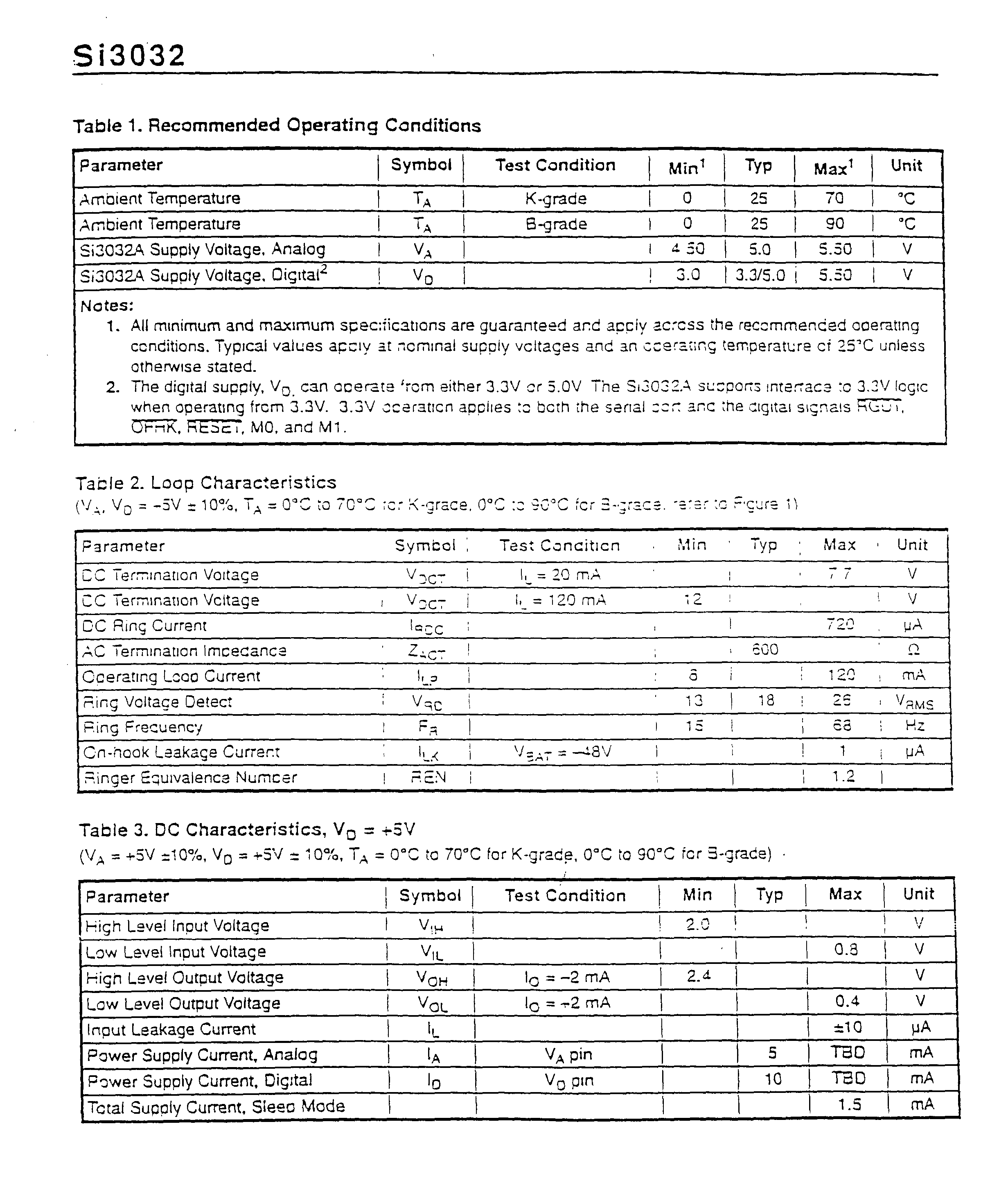


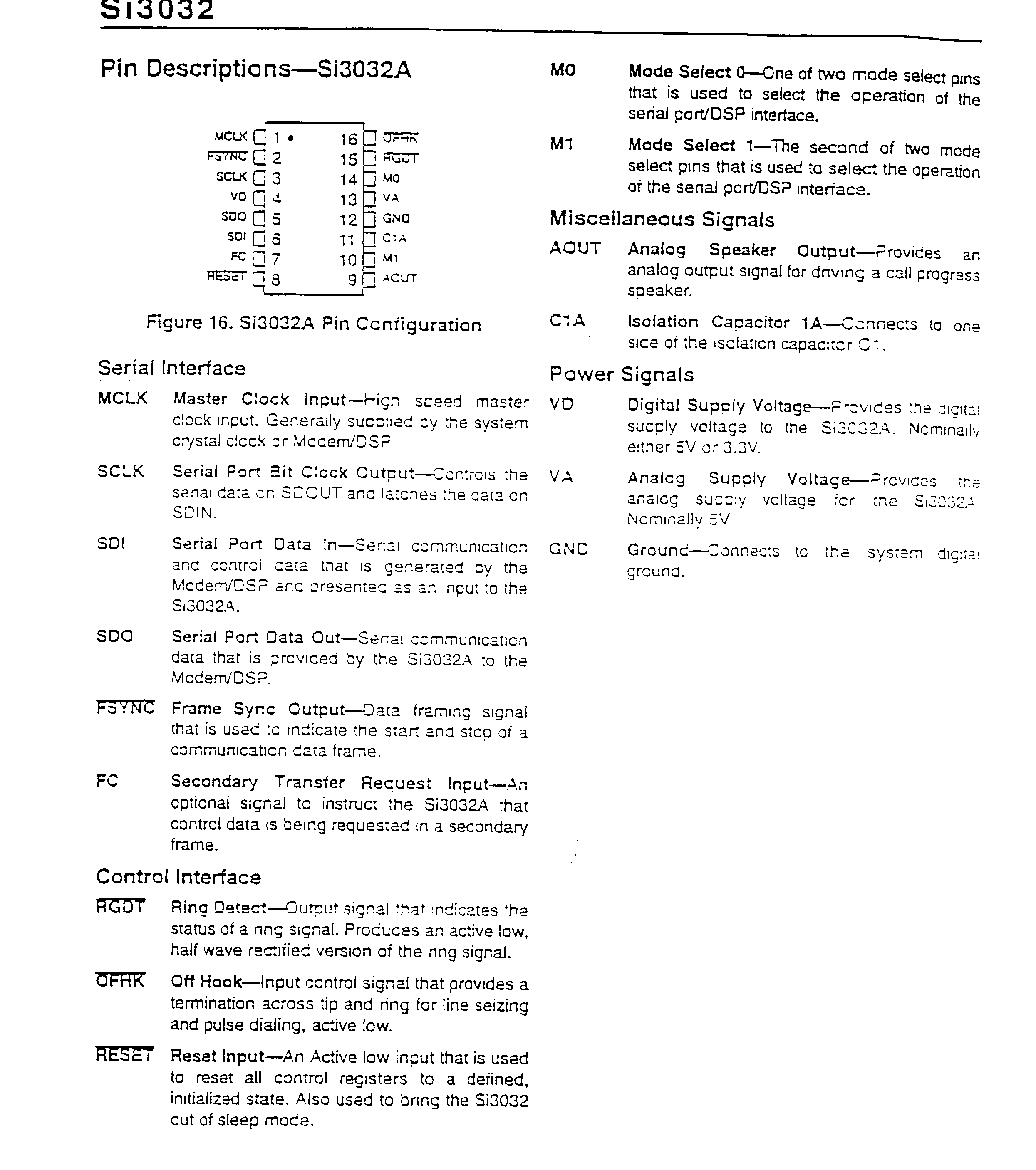


- Further modifications and alternative embodiments of this invention will be apparent to those skilled in the art in view of this description. Accordingly, this description is to be construed as illustrative only and is for the purpose of teaching those skilled in the art the manner of carrying out the invention. It is to be understood that the forms of the invention herein shown and described are to be taken as the presently preferred embodiments. Various changes may be made in the shape, size and arrangement of parts. For example, equivalent elements may be substituted for those Illustrated and described herein, and certain features of the invention may be utilized independently of the use of other features, all as would be apparent to one skilled in the art after having the benefit of this description of the invention.
Claims (55)
1. Digital direct access arrangement circuitry for terminating a phone line connection, comprising:
powered side circuitry operable to communicate digitally with phone line side circuitry, said digital communication comprising a digital data stream in a pulse density modulation format transmitted across an isolation barrier; and
phone line side circuitry operable to communicate digitally with powered side circuitry, said digital communication comprising a digital data stream in a pulse density modulation format transmitted across said isolation barrier.
2. The digital direct access arrangement circuitry of claim 1 , wherein communication across said isolation barrier is bi-directional.
3. The digital direct access arrangement circuitry of claim 2 , further comprising an isolation barrier coupled between said powered side circuitry and said phone line side circuitry.
4. The digital direct access arrangement circuitry of claim 2 , wherein said isolation barrier comprises one or more capacitors.
5. The digital direct access arrangement circuitry of claim 2 , wherein said powered side circuitry includes encode circuitry coupled to said digital data stream to generate an encoded digital signal for transmission across said isolation barrier and wherein said phone line circuitry includes decode circuitry to generate a decoded digital signal from said encoded digital signal.
6. The digital direct access arrangement circuitry of claim 2 , wherein said encoded digital signal comprises control data added to said digital data stream.
7. The digital direct access arrangement circuitry of claim 2 , wherein said encoded digital signal comprises framing data added to said digital data stream for data synchronization within said phone line side circuitry.
8. The digital direct access arrangement circuitry of claim 2 , wherein said encoded digital signal comprises said digital data stream formatted such that said decode circuitry may recover a clock signal from said encoded digital signal.
9. The digital direct access arrangement circuitry of claim 2 , wherein said phone line side circuitry includes encode circuitry coupled to said digital data to generate an encoded digital signal for transmission across said isolation barrier and said powered circuitry includes decode circuitry to generate a decoded digital signal from said encoded digital signal.
10. The digital direct access arrangement circuitry of claim 2 , wherein said encoded digital signal comprises control data added to said digital data stream.
11. The digital direct access arrangement circuitry of claim 2 wherein said control data comprises phone line status information.
12. The digital direct access arrangement circuitry of claim 2 . wherein said powered side circuitry has a communication interface that may be coupled to an external device.
13. The digital direct access arrangement circuitry of claim 2 , wherein said phone line side circuitry has analog output signals that may be coupled to phone lines through hook-switch circuitry and diode bridge circuitry.
14. Powered side circuitry for digital direct access arrangement circuitry for terminating a phone line connection, comprising:
a communication interface that may be coupled to an external device;
an isolation interface that may communicate digitally with phone line side circuitry through an isolation barrier; and
encode circuitry within said isolation interface to generate an encoded digital signal from a digital data stream for transmission across said isolation barrier.
15. The powered side circuitry of claim 14 , wherein said encoded digital signal comprises control data added to said digital data stream.
16. The powered side circuitry of claim 14 , wherein said encoded digital signal comprises framing data added to said digital data stream for data synchronization within said phone line side circuitry.
17. The powered side circuitry of claim 14 , wherein said encoded digital signal comprises said digital data stream formatted such that said decode circuitry may recover a clock signal from said encoded digital signal.
18. The powered side circuitry of claim 14 , wherein said digital data signal is a digital data stream in a pulse density modulation format.
19. The powered side circuitry of claim 14 , wherein said isolation interface may communicate bidirectionally across said isolation barrier.
20. The powered side circuitry of claim 14 , wherein signals communicated through said communication interface comprises digital data signals, control signals and phone line status signals
21. The powered side circuitry of claim 20 , wherein said communication interface comprises a digital senal port interface.
22. The powered side circuitry of claim 14 , further comprising an over sampled delta-sigma modulator coupled to receive base-band digital data signals from said external device and to convert said base-band digital data signals to a digital data stream in a pulse density modulation format.
23. The powered side circuitry of claim 14 , further comprising decode circuitry that may be coupled to an encoded digital signal received from said phone line side circuitry to generate a decoded digital signal.
24. The powered side circuitry of claim 23 , wherein said decoded digital signal comprises a digital data stream in a pulse density modulation format, and further comprising a digital filter coupled to said digital data stream to generate base-band digital data signals.
25. Phone line side circuitry for digital direct access arrangement circuitry for terminating a phone line connection, comprising:
a communication interface that may be coupled to phone lines;
an isolation interface that may communicate digitally with powered side circuitry through an isolation barrier; and
decode circuitry within said isolation interface to generate a decoded digital signal from an encoded digital signal received from said powered side circuitry across said isolation barrier.
26. The phone line side circuitry of claim 25 , wherein said encoded digital signal comprises a digital data stream formatted such that said decode circuitry may recover a clock signal from said encoded digital signal.
27. The phone line side circuitry of claim 25 , wherein said encoded digital signal comprises control data added to a digital data stream.
28. The phone line side circuitry of claim 25 , wherein said encoded digital signal comprises framing data added to a digital data stream for data synchronization within said phone line side circuitry.
29. The phone line side circuitry of claim 25 , wherein said isolation interface may communicate bidirectionally across said isolation barrier.
30. The phone line side circuitry of claim 25 , wherein signals communicated through said communication interface comprises analog data signals.
31. The phone line side circuitry of claim 25 , wherein said communication interface is configured to be coupled to phone lines through external hook-switch circuitry and an external diode bridge.
32. The phone line side circuitry of claim 25 , wherein said communication interface comprises circuitry coupled to said phone lines to detect ringing on said phone-lines and to control an off-hook state on said phone lines.
33. The phone line side circuitry of claim 32 , wherein said communication interface comprises DC termination circuitry coupled to said phone lines to provide an internal DC power supply to said phone line side circuitry.
34. The phone line side circuitry of claim 25 , further comprising an over sampled delta-sigma analog-to-digital converter configured to be coupled to analog signals received from said phone lines to convert said analog signals to a digital data stream in a pulse density modulation format.
35. The phone line side circuitry of claim 25 , further comprising encode circuitry within said isolation interface to generate an encoded digital signal from a digital data stream for transmission across said isolation barrier.
36. The phone line side circuitry of claim 35 , wherein said encoded digital signal comprises control data added to said digital data stream.
37. The phone line side circuitry of claim 35 , wherein said control data comprises phone line status information.
38. The phone line side circuitry of claim 25 , wherein said digital data signal is a digital data stream in a pulse density modulation format.
39. A method for communicating with phone lines, comprising:
converting a signal received from phone lines into a digital data stream in a pulse density modulation format;
communicating said digital data stream across an isolation barrier from phone line side circuitry to powered side circuitry;
40. The method of claim 39 , wherein said isolation barrier comprises one or more capacitors.
41. The method of claim 40 , further comprising:
communicating a digital bit stream across said isolation barrier from said powered side circuitry to said phone line side circuitry; and
recovery a clock signal within said phone line side circuitry from said digital bit stream.
42. The method of claim 40 , further comprising:
encoding said digital data stream prior to said communicating step.
43. A method for communicating with phone lines, comprising:
converting a digital signal into a digital data stream in a pulse density modulation format; and
communicating said digital data stream across an isolation barrier from powered side circuitry to phone line side circuitry.
44. The method of claim 43 , wherein said isolation barrier comprises one or more capacitors.
45. The method of claim 44 , further comprising:
recovery a clock signal within said phone line side circuitry from said digital bit stream.
46. The method of claim 45 , further comprising:
encoding said digital data stream prior to said communicating step.
47. A method for communicating with phone lines, comprising
generating an encoded digital signal from a digital data signal: and
communicating said encoded digital signal across an isolation barrier from phone line side circuitry to powered side circuitry.
48. The method of claim 47 , wherein said generating step comprises adding control data and phone line status information to said digital data stream.
49. The method of claim 47 , further comprising:
communicating a digital bit stream across said isolation barrier from said powered side circuitry to said phone line side circuitry; and
recovery a clock signal within said phone line side circuitry from said digital bit stream.
50. The method of claim 49 . wherein said isolation barrier comprises one or more capacitors.
51. A method for communicating with phone lines, comprising:
generating an encoded digital signal from a digital data signal; and
communicating said encoded digital signal across an isolation barrier from powered side circuitry to phone line side circuitry.
52. The method of claim 51 , wherein said generating step comprises adding control data and synchronization framing information to said digital data stream.
53. The method of claim 51 , wherein said generating step comprises formatting said digital data stream so that a clock signal may be recovered from said encoded digital signal.
54. The method of claim 53 , wherein said generating step comprises adding control data and synchronization framing information to said digital data stream
55. The method of claim 54 , wherein said isolation barrier comprises one or more capacitors
Priority Applications (4)
| Application Number | Priority Date | Filing Date | Title |
|---|---|---|---|
| US10/227,104 US7072389B2 (en) | 1997-04-22 | 2002-08-23 | Direct digital access arrangement circuitry and method for connecting to phone lines |
| US10/780,219 US7301995B2 (en) | 1997-04-22 | 2004-02-17 | Direct digital access arrangement circuitry and method for connecting to phone lines |
| US10/780,142 US7283584B2 (en) | 1997-04-22 | 2004-02-17 | Direct digital access arrangement circuitry and method for connecting to phone lines |
| US11/398,090 US7463675B2 (en) | 1997-04-22 | 2006-04-05 | Direct digital access arrangement circuitry and method for connecting to phone lines |
Applications Claiming Priority (6)
| Application Number | Priority Date | Filing Date | Title |
|---|---|---|---|
| US08/841,409 US6137827A (en) | 1997-04-22 | 1997-04-22 | Isolation system with digital communication across a capacitive barrier |
| US08/837,714 US6430229B1 (en) | 1997-04-22 | 1997-04-22 | Capacitive isolation system with digital communication and power transfer |
| US08/837,702 US5870046A (en) | 1997-04-22 | 1997-04-22 | Analog isolation system with digital communication across a capacitive barrier |
| US09/035,175 US6385235B1 (en) | 1997-04-22 | 1998-03-04 | Direct digital access arrangement circuitry and method for connecting to phone lines |
| US10/127,285 US7200167B2 (en) | 1997-04-22 | 2002-04-22 | Direct digital access arrangement circuitry and method for connecting to phone lines |
| US10/227,104 US7072389B2 (en) | 1997-04-22 | 2002-08-23 | Direct digital access arrangement circuitry and method for connecting to phone lines |
Related Parent Applications (1)
| Application Number | Title | Priority Date | Filing Date |
|---|---|---|---|
| US10/127,285 Continuation US7200167B2 (en) | 1997-04-22 | 2002-04-22 | Direct digital access arrangement circuitry and method for connecting to phone lines |
Related Child Applications (3)
| Application Number | Title | Priority Date | Filing Date |
|---|---|---|---|
| US10/780,219 Continuation US7301995B2 (en) | 1997-04-22 | 2004-02-17 | Direct digital access arrangement circuitry and method for connecting to phone lines |
| US10/780,142 Continuation US7283584B2 (en) | 1997-04-22 | 2004-02-17 | Direct digital access arrangement circuitry and method for connecting to phone lines |
| US11/398,090 Continuation US7463675B2 (en) | 1997-04-22 | 2006-04-05 | Direct digital access arrangement circuitry and method for connecting to phone lines |
Publications (2)
| Publication Number | Publication Date |
|---|---|
| US20030002571A1 true US20030002571A1 (en) | 2003-01-02 |
| US7072389B2 US7072389B2 (en) | 2006-07-04 |
Family
ID=27488274
Family Applications (7)
| Application Number | Title | Priority Date | Filing Date |
|---|---|---|---|
| US09/035,175 Expired - Lifetime US6385235B1 (en) | 1997-04-22 | 1998-03-04 | Direct digital access arrangement circuitry and method for connecting to phone lines |
| US09/470,273 Expired - Fee Related US6654409B1 (en) | 1997-04-22 | 1999-12-22 | Direct digital access arrangement circuitry and method for connecting DSL circuitry to phone lines |
| US10/127,285 Expired - Fee Related US7200167B2 (en) | 1997-04-22 | 2002-04-22 | Direct digital access arrangement circuitry and method for connecting to phone lines |
| US10/227,104 Expired - Fee Related US7072389B2 (en) | 1997-04-22 | 2002-08-23 | Direct digital access arrangement circuitry and method for connecting to phone lines |
| US10/780,219 Expired - Fee Related US7301995B2 (en) | 1997-04-22 | 2004-02-17 | Direct digital access arrangement circuitry and method for connecting to phone lines |
| US10/780,142 Expired - Fee Related US7283584B2 (en) | 1997-04-22 | 2004-02-17 | Direct digital access arrangement circuitry and method for connecting to phone lines |
| US11/398,090 Expired - Fee Related US7463675B2 (en) | 1997-04-22 | 2006-04-05 | Direct digital access arrangement circuitry and method for connecting to phone lines |
Family Applications Before (3)
| Application Number | Title | Priority Date | Filing Date |
|---|---|---|---|
| US09/035,175 Expired - Lifetime US6385235B1 (en) | 1997-04-22 | 1998-03-04 | Direct digital access arrangement circuitry and method for connecting to phone lines |
| US09/470,273 Expired - Fee Related US6654409B1 (en) | 1997-04-22 | 1999-12-22 | Direct digital access arrangement circuitry and method for connecting DSL circuitry to phone lines |
| US10/127,285 Expired - Fee Related US7200167B2 (en) | 1997-04-22 | 2002-04-22 | Direct digital access arrangement circuitry and method for connecting to phone lines |
Family Applications After (3)
| Application Number | Title | Priority Date | Filing Date |
|---|---|---|---|
| US10/780,219 Expired - Fee Related US7301995B2 (en) | 1997-04-22 | 2004-02-17 | Direct digital access arrangement circuitry and method for connecting to phone lines |
| US10/780,142 Expired - Fee Related US7283584B2 (en) | 1997-04-22 | 2004-02-17 | Direct digital access arrangement circuitry and method for connecting to phone lines |
| US11/398,090 Expired - Fee Related US7463675B2 (en) | 1997-04-22 | 2006-04-05 | Direct digital access arrangement circuitry and method for connecting to phone lines |
Country Status (7)
| Country | Link |
|---|---|
| US (7) | US6385235B1 (en) |
| EP (2) | EP0978190B1 (en) |
| JP (1) | JP4054068B2 (en) |
| KR (1) | KR100380790B1 (en) |
| AU (1) | AU7468198A (en) |
| DE (3) | DE69835465T2 (en) |
| WO (1) | WO1998048541A2 (en) |
Cited By (1)
| Publication number | Priority date | Publication date | Assignee | Title |
|---|---|---|---|---|
| US20090110056A1 (en) * | 2007-10-26 | 2009-04-30 | Satoshi Miyaji | Moving-picture compression-encoding apparatus |
Families Citing this family (77)
| Publication number | Priority date | Publication date | Assignee | Title |
|---|---|---|---|---|
| US6587560B1 (en) * | 1997-04-22 | 2003-07-01 | Silicon Laboratories Inc. | Low voltage circuits powered by the phone line |
| US6385235B1 (en) * | 1997-04-22 | 2002-05-07 | Silicon Laboratories, Inc. | Direct digital access arrangement circuitry and method for connecting to phone lines |
| US6442213B1 (en) * | 1997-04-22 | 2002-08-27 | Silicon Laboratories Inc. | Digital isolation system with hybrid circuit in ADC calibration loop |
| US6167134A (en) * | 1997-04-22 | 2000-12-26 | Silicon Laboratories, Inc. | External resistor and method to minimize power dissipation in DC holding circuitry for a communication system |
| US6339048B1 (en) * | 1999-12-23 | 2002-01-15 | Elementis Specialties, Inc. | Oil and oil invert emulsion drilling fluids with improved anti-settling properties |
| US6714590B1 (en) | 1999-07-23 | 2004-03-30 | Silicon Laboratories, Inc. | Integrated modem and line-isolation circuitry and associated method |
| US6724891B1 (en) * | 1998-03-04 | 2004-04-20 | Silicon Laboratories Inc. | Integrated modem and line-isolation circuitry and associated method powering caller ID circuitry with power provided across an isolation barrier |
| US6757381B1 (en) * | 1998-08-13 | 2004-06-29 | Eugene Robert Worley | Design of telephone line interface circuits using a two chip opto-coupler with LEDs integrated onto silicon chips |
| US6920218B1 (en) * | 1998-11-16 | 2005-07-19 | Agere Systems Inc. | Combination clock and charge pump for line powered DAA |
| US6553118B1 (en) * | 1999-05-11 | 2003-04-22 | Agere Systems Inc. | Method and apparatus for calculating DC offset in a digital gyrator |
| US6304597B1 (en) | 1999-07-23 | 2001-10-16 | Silicon Laboratories, Inc. | Integrated modem and line-isolation circuitry with selective modem processing and associated method |
| US6826225B1 (en) | 1999-07-23 | 2004-11-30 | Silicon Laboratories, Inc. | Integrated modem and line-isolation circuitry with selective raw data or modem data communication and associated method |
| US6735246B1 (en) | 1999-07-23 | 2004-05-11 | Silicon Laboratories Inc. | Integrated modem and line-isolation circuitry with data flow control and associated method |
| US7020187B1 (en) | 1999-07-23 | 2006-03-28 | Silicon Laboratories Inc. | Integrated modem and line-isolation circuitry with HDLC framing and associated method |
| US6853644B1 (en) * | 1999-12-22 | 2005-02-08 | Intel Corporation | Method and apparatus for driving data packets |
| US6262600B1 (en) * | 2000-02-14 | 2001-07-17 | Analog Devices, Inc. | Isolator for transmitting logic signals across an isolation barrier |
| US7526206B1 (en) * | 2000-05-23 | 2009-04-28 | The Aerospace Corporation | Laser communications crosslink system |
| US6510215B1 (en) | 2000-07-17 | 2003-01-21 | Silicon Laboratories Inc. | Caller ID data-reporting mechanism for electronic devices and associated methods |
| US6748515B1 (en) | 2000-07-17 | 2004-06-08 | Silicon Laboratories Inc. | Programmable vendor identification circuitry and associated method |
| US7024539B2 (en) * | 2000-07-17 | 2006-04-04 | Silicon Laboratories Inc. | Resistor identification configuration circuitry and associated method |
| US7058173B2 (en) * | 2001-02-28 | 2006-06-06 | Thomson Licensing | Multi-stage isolation barrier circuitry and method for connection of a telephony device to a telephone line |
| EP1276305A1 (en) * | 2001-05-30 | 2003-01-15 | Texas Instruments Incorporated | Modem isolation systems and apparatus |
| US20030012363A1 (en) * | 2001-07-16 | 2003-01-16 | Loeb Frederick F. | Jack module with integrated modem interface circuits |
| US7139391B2 (en) * | 2001-10-30 | 2006-11-21 | Integration Associates, Inc. | DAA hook switch |
| US7702293B2 (en) * | 2001-11-02 | 2010-04-20 | Nokia Corporation | Multi-mode I/O circuitry supporting low interference signaling schemes for high speed digital interfaces |
| US7277491B2 (en) * | 2002-05-14 | 2007-10-02 | Ess Technology, Inc. | Data access arrangement using a high frequency transformer for electrical isolation |
| US8315348B2 (en) * | 2002-06-21 | 2012-11-20 | Gvbb Holdings S.A.R.L. | Clock extraction circuit for use in a linearly expandable broadcast router |
| DE10243197B4 (en) | 2002-09-18 | 2011-05-05 | Infineon Technologies Ag | Digital signal transmission method |
| KR20040074868A (en) * | 2003-02-19 | 2004-08-26 | 삼성전자주식회사 | Apparatus and method for transmitting voice data on ADSL subscriber card |
| US7266195B1 (en) | 2003-03-04 | 2007-09-04 | Silicon Laboratories Inc. | Surge clamp protection circuit |
| US6901059B2 (en) * | 2003-03-10 | 2005-05-31 | Utstarcom, Inc. | Low noise hybrid circuit for communications systems using time division multiplexing |
| US7089475B1 (en) | 2003-03-26 | 2006-08-08 | Silicon Laboratories Inc. | Error correction of data across an isolation barrier |
| US6968055B1 (en) | 2003-03-26 | 2005-11-22 | Silicon Laboratories Inc. | DC holding circuit |
| US7218713B1 (en) | 2003-04-15 | 2007-05-15 | Silicon Laboratories Inc. | Telephone line interface for DAA circuitry |
| US6891935B1 (en) | 2003-12-16 | 2005-05-10 | Silicon Laboratories Inc. | Direct access arrangement (DAA) circuit having automatic interface identification |
| US7512175B2 (en) * | 2005-03-16 | 2009-03-31 | Ibiquity Digital Corporation | Method for synchronizing exporter and exciter clocks |
| ES2705589T3 (en) | 2005-04-22 | 2019-03-26 | Qualcomm Inc | Systems, procedures and devices for smoothing the gain factor |
| US7672448B2 (en) * | 2005-06-23 | 2010-03-02 | 2Wire, Inc. | Network interface device with a remote power source |
| US8213489B2 (en) * | 2005-06-23 | 2012-07-03 | Agere Systems Inc. | Serial protocol for agile sample rate switching |
| US7773733B2 (en) * | 2005-06-23 | 2010-08-10 | Agere Systems Inc. | Single-transformer digital isolation barrier |
| US7940921B2 (en) * | 2005-06-23 | 2011-05-10 | Agere Systems Inc. | Continuous power transfer scheme for two-wire serial link |
| US7526034B2 (en) * | 2006-04-18 | 2009-04-28 | 2Wire, Inc. | Method and apparatus for communicating between devices having no common electrical ground |
| US7965977B2 (en) * | 2006-04-18 | 2011-06-21 | 2Wire, Inc. | Remote antenna system |
| US8520835B2 (en) * | 2006-04-18 | 2013-08-27 | 2Wire, Inc. | Method and apparatus for providing power to a network interface device via telephone lines |
| US20080279288A1 (en) * | 2007-05-11 | 2008-11-13 | Philip John Crawley | Digital Isolator Interface with Process Tracking |
| US7732889B2 (en) * | 2007-05-24 | 2010-06-08 | Akros Silicon Inc. | Capacitor structure in a semiconductor device |
| US20080277761A1 (en) * | 2007-05-08 | 2008-11-13 | Texas Instruments, Inc. | On-chip isolation capacitors, circuits therefrom, and methods for forming the same |
| US20090145628A1 (en) * | 2007-12-05 | 2009-06-11 | Karl Gifford | Method of using finely stranded 32-56 gauge "Litz Wire" in both the construction of the Megasonic amplifier (including but not limited to the power transformer and the output filter magnetics) and the interconnect cabling from the amplifier to the transducer, utilizing frequencies above 500kHz to 5 MHz and beyond, but not limited to these frequencies |
| US7804859B2 (en) * | 2008-06-30 | 2010-09-28 | Silicon Laboratories, Inc. | System and method of providing electrical isolation |
| US8095710B2 (en) * | 2008-06-30 | 2012-01-10 | Silicon Laboratories Inc. | System and method of providing electrical isolation |
| US7675444B1 (en) * | 2008-09-23 | 2010-03-09 | Maxim Integrated Products, Inc. | High voltage isolation by capacitive coupling |
| US8150028B2 (en) * | 2008-12-17 | 2012-04-03 | Silicon Laboratories, Inc. | Circuit device with serial bus isolation |
| US8207635B2 (en) * | 2009-02-20 | 2012-06-26 | Redwood Systems, Inc. | Digital switch communication |
| US8427300B2 (en) * | 2009-02-20 | 2013-04-23 | Redwood Systems, Inc. | Transmission of power and data with frequency modulation |
| US8248230B2 (en) | 2009-02-20 | 2012-08-21 | Redwood Systems, Inc. | Smart power device |
| US8058750B2 (en) * | 2009-05-14 | 2011-11-15 | Redwood Systems, Inc. | Discharge cycle communication |
| JP2011160096A (en) * | 2010-01-29 | 2011-08-18 | Toshiba Corp | Optical transmission circuit, optical reception circuit, and optically coupled isolation circuit |
| TWI445314B (en) * | 2010-08-24 | 2014-07-11 | Genesys Logic Inc | Transceiver system having phase and frequency detector and method thereof |
| DE102010042903A1 (en) * | 2010-10-26 | 2012-04-26 | Robert Bosch Gmbh | Transmission method and system |
| EP2629438B1 (en) | 2012-02-15 | 2014-11-19 | ams AG | Transmitter and receiver for pulse density modulated signals and signal processing method |
| US9013425B2 (en) * | 2012-02-23 | 2015-04-21 | Cypress Semiconductor Corporation | Method and apparatus for data transmission via capacitance sensing device |
| US8896182B2 (en) * | 2012-04-05 | 2014-11-25 | General Electric Corporation | System for driving a piezoelectric load and method of making same |
| US9293997B2 (en) | 2013-03-14 | 2016-03-22 | Analog Devices Global | Isolated error amplifier for isolated power supplies |
| US10097243B2 (en) * | 2013-03-15 | 2018-10-09 | David Schie | Isolator |
| DE102013103362B4 (en) * | 2013-04-04 | 2016-09-01 | eesy-ic GmbH | CONVERTER ARRANGEMENT |
| US10536309B2 (en) | 2014-09-15 | 2020-01-14 | Analog Devices, Inc. | Demodulation of on-off-key modulated signals in signal isolator systems |
| US10270630B2 (en) | 2014-09-15 | 2019-04-23 | Analog Devices, Inc. | Demodulation of on-off-key modulated signals in signal isolator systems |
| US9660848B2 (en) | 2014-09-15 | 2017-05-23 | Analog Devices Global | Methods and structures to generate on/off keyed carrier signals for signal isolators |
| CN107078977B (en) | 2014-09-24 | 2020-10-16 | 美国亚德诺半导体公司 | Circuit and system for multipath isolator communication |
| US9998301B2 (en) | 2014-11-03 | 2018-06-12 | Analog Devices, Inc. | Signal isolator system with protection for common mode transients |
| US9065461B1 (en) * | 2015-01-15 | 2015-06-23 | Avago Technologies General Ip (Singapore) Pte. Ltd. | Coding and decoding isolation device and method thereof |
| US9941999B1 (en) * | 2017-03-08 | 2018-04-10 | Allegro Microsystems, Llc | Methods and apparatus for communication over an isolation barrier with monitoring |
| US10943855B2 (en) | 2017-08-23 | 2021-03-09 | Semiconductor Components Industries, Llc | Electronic device packaging with galvanic isolation |
| US10554456B2 (en) | 2017-08-23 | 2020-02-04 | Semiconductor Components Industries, Llc | Circuits and methods for bi-directional data communication over isolation channels |
| US10097166B1 (en) | 2017-10-13 | 2018-10-09 | Hamilton Sundstrand Corporation | Transformer coupled control isolation for direct current control signals |
| WO2020189068A1 (en) * | 2019-03-18 | 2020-09-24 | パナソニックIpマネジメント株式会社 | Capacitive coupling circuit device |
| US11115244B2 (en) | 2019-09-17 | 2021-09-07 | Allegro Microsystems, Llc | Signal isolator with three state data transmission |
Citations (99)
| Publication number | Priority date | Publication date | Assignee | Title |
|---|---|---|---|---|
| US3750024A (en) * | 1971-06-16 | 1973-07-31 | Itt Corp Nutley | Narrow band digital speech communication system |
| US4066843A (en) * | 1975-03-28 | 1978-01-03 | Applied Data Research, Inc. | Telephone circuit monitoring system |
| US4192978A (en) * | 1978-02-27 | 1980-03-11 | Vincent Ogden W | Operational amplifier hybrid system |
| US4216426A (en) * | 1979-03-02 | 1980-08-05 | Burroughs Corporation | Self-clocked data transmission system having automatic signal reversing means |
| US4271526A (en) * | 1979-03-02 | 1981-06-02 | Burroughs Corporation | Three-level, self-clocked data transmission system |
| US4384274A (en) * | 1979-06-22 | 1983-05-17 | American Microsystems, Inc. | Current mirror digital to analog converter |
| US4393516A (en) * | 1979-03-09 | 1983-07-12 | Electric Power Research Institute, Inc. | Data transmission system and method |
| US4433212A (en) * | 1982-06-21 | 1984-02-21 | Applied Spectrum Technologies, Inc. | Telephone line interface circuit |
| US4465903A (en) * | 1983-04-21 | 1984-08-14 | Ixo, Inc. | Electronic telephone interface circuit |
| US4528664A (en) * | 1982-11-29 | 1985-07-09 | Northern Telecom Limited | Call progress signal monitor and method for telephone systems |
| US4529845A (en) * | 1984-04-02 | 1985-07-16 | Gte Communication Systems Corporation | Optical coupling interface circuit for telephone line ringing signal indication or detection |
| US4567331A (en) * | 1983-12-22 | 1986-01-28 | Itt Corporation | Electronic hybrid having synthesized impedance circuitry |
| US4594577A (en) * | 1980-09-02 | 1986-06-10 | American Microsystems, Inc. | Current mirror digital to analog converter |
| US4607170A (en) * | 1985-03-01 | 1986-08-19 | Digitel, Inc. | Data communication interconnect device |
| US4644526A (en) * | 1984-11-13 | 1987-02-17 | Chialin Wu | Full duplex frequency division multiplex communication system |
| US4656661A (en) * | 1984-12-13 | 1987-04-07 | American Telephone And Telegraph Company | Switched capacitor coupled line receiver circuit |
| US4686697A (en) * | 1983-11-21 | 1987-08-11 | Lifeline Systems, Inc. | Telephone care system with telephone line-checking |
| US4686699A (en) * | 1984-12-21 | 1987-08-11 | International Business Machines Corporation | Call progress monitor for a computer telephone interface |
| US4720811A (en) * | 1985-04-26 | 1988-01-19 | Hitachi, Ltd. | Microprocessor capable of stopping its operation at any cycle time |
| US4741031A (en) * | 1986-06-27 | 1988-04-26 | Gai-Tronics | Intrinsically safe telephone |
| US4757528A (en) * | 1986-09-05 | 1988-07-12 | Harris Corporation | Thermally coupled information transmission across electrical isolation boundaries |
| US4835486A (en) * | 1986-04-28 | 1989-05-30 | Burr-Brown Corporation | Isolation amplifier with precise timing of signals coupled across isolation barrier |
| US4843339A (en) * | 1987-10-28 | 1989-06-27 | Burr-Brown Corporation | Isolation amplifier including precision voltage-to-duty-cycle converter and low ripple, high bandwidth charge balance demodulator |
| US4901217A (en) * | 1987-12-01 | 1990-02-13 | Apple Computer, Inc. | Digital input power supply and method |
| US4901275A (en) * | 1986-12-18 | 1990-02-13 | Burr-Brown Limited | Analog data acquisition apparatus and method provided with electro-optical isolation |
| US4943807A (en) * | 1988-04-13 | 1990-07-24 | Crystal Semiconductor | Digitally calibrated delta-sigma analog-to-digital converter |
| US4993063A (en) * | 1987-03-03 | 1991-02-12 | Kiko Frederick J | Channel unit interface circuit |
| US4995111A (en) * | 1987-06-19 | 1991-02-19 | Fujitsu Limited | Ring trip circuit for subscriber telephone |
| US4996529A (en) * | 1989-04-10 | 1991-02-26 | Motorola, Inc. | Auto-zeroing circuit for offset cancellation |
| US5012950A (en) * | 1988-04-30 | 1991-05-07 | Holger Knappe | Plastic container for liquids or gases |
| US5032819A (en) * | 1988-10-24 | 1991-07-16 | Murata Mfg. Co., Ltd. | Data communications system |
| US5086454A (en) * | 1989-11-17 | 1992-02-04 | Vocal Technologies, Ltd. | Direct connect modem deriving power from telephone line |
| US5097503A (en) * | 1989-01-31 | 1992-03-17 | Alcatel Cit | Electronic subscriber line connection circuit |
| US5136630A (en) * | 1990-07-13 | 1992-08-04 | Gai-Tronics | Intrinsically safe telephone |
| US5204896A (en) * | 1990-08-10 | 1993-04-20 | Telegenics, Inc. | Outbound telemetry device |
| US5224154A (en) * | 1991-09-06 | 1993-06-29 | Universal Data Systems, Inc. | Line powered DCA including dual programmed microcontrollers |
| US5235634A (en) * | 1990-12-14 | 1993-08-10 | Telegenics, Inc. | Apparatus and method for activating an inbound telemetry device |
| US5237511A (en) * | 1990-10-29 | 1993-08-17 | Westronic, Inc. | Distribution automation smart remote terminal unit |
| US5287107A (en) * | 1992-06-05 | 1994-02-15 | Hewlett-Packard Company | Optical isolation amplifier with sigma-delta modulation |
| US5311588A (en) * | 1991-02-19 | 1994-05-10 | Intervoice, Inc. | Call progress detection circuitry and method |
| US5323398A (en) * | 1991-10-24 | 1994-06-21 | Nec Corporation | Transmission system for transmitting G3 facsimile signals and compressed speech signals |
| US5323451A (en) * | 1989-11-29 | 1994-06-21 | Sharp Kabushiki Kaisha | Facsimile device and automatic receiving method thereof |
| US5329585A (en) * | 1992-11-30 | 1994-07-12 | Motorola, Inc. | Subscriber line interface circuit for controlling AC and DC output impedance |
| US5329281A (en) * | 1992-04-30 | 1994-07-12 | Hewlett-Packard Company | Analog to digital converter with autoranging offset |
| US5333196A (en) * | 1991-04-15 | 1994-07-26 | Northern Telecom Limited | Current limiting battery feed arrangement |
| US5337338A (en) * | 1993-02-01 | 1994-08-09 | Qualcomm Incorporated | Pulse density modulation circuit (parallel to serial) comparing in a nonsequential bit order |
| US5343516A (en) * | 1989-09-29 | 1994-08-30 | Digital Systems Group, Inc. | Computer telecommunications signalling interface |
| US5384808A (en) * | 1992-12-31 | 1995-01-24 | Apple Computer, Inc. | Method and apparatus for transmitting NRZ data signals across an isolation barrier disposed in an interface between adjacent devices on a bus |
| US5390249A (en) * | 1991-03-14 | 1995-02-14 | Park; Chung H. | Receiver device for receiving ringing signals in an off-hook line condition |
| US5406283A (en) * | 1992-05-01 | 1995-04-11 | University Of Waterloo | Multi-bit oversampled DAC with dynamic element matching |
| US5410594A (en) * | 1990-03-02 | 1995-04-25 | Kabushiki Kaisha Toshiba | Transmission input/output device with reduced power consumption |
| US5426698A (en) * | 1993-05-11 | 1995-06-20 | General Datacomm, Inc. | Transformed current sensing relay for use in switched network modems and circuit incorporating same |
| US5428682A (en) * | 1993-03-12 | 1995-06-27 | Advanced Micro Devices, Inc. | Subscriber line interface circuit with reduced on-chip power dissipation |
| US5438678A (en) * | 1993-03-23 | 1995-08-01 | Smith; Peter L. | Self-powered computer accessory device for power extraction from attached data signals and method of operating thereof |
| US5442694A (en) * | 1994-04-12 | 1995-08-15 | Dialogic Corporation | Ring tone detection for a telephone system |
| US5500895A (en) * | 1994-05-24 | 1996-03-19 | Yurgelites; Gerald J. | Telephone isolation device |
| US5500894A (en) * | 1993-12-03 | 1996-03-19 | Silicon Systems, Inc. | Telephone line interface with AC and DC transconductance loops |
| US5506900A (en) * | 1993-02-17 | 1996-04-09 | Silicon Systems, Inc. | Temperature compensation for trans-hybrid loss in a miniaturized data access arrangement |
| US5506903A (en) * | 1993-04-06 | 1996-04-09 | Sony Corporation | Digital multiplex transmission system |
| US5509068A (en) * | 1994-03-25 | 1996-04-16 | Bayless; Samuel R. | Electronic ring monitoring device for telecommunications line |
| US5511118A (en) * | 1991-01-31 | 1996-04-23 | Northern Telecom Limited | Method of providing d.c. feed to a telephone line |
| US5521967A (en) * | 1990-04-24 | 1996-05-28 | The Telephone Connection, Inc. | Method for monitoring telephone call progress |
| US5533053A (en) * | 1994-05-16 | 1996-07-02 | Silicon Systems, Inc. | Low frequency common mode rejection in a clock circuit |
| US5544241A (en) * | 1995-06-27 | 1996-08-06 | Andrew S. Dibner | Telephone ring detector |
| US5546448A (en) * | 1994-11-10 | 1996-08-13 | Multi-Tech Systems, Inc. | Apparatus and method for a caller ID modem interface |
| US5592529A (en) * | 1994-09-29 | 1997-01-07 | International Business Machines Corporation | Telephone inadvertent off-hook condition detector |
| US5598157A (en) * | 1994-10-28 | 1997-01-28 | Harris Corporation | Sigma Delta analog to digital converter with three point calibration apparatus and method |
| US5600551A (en) * | 1995-08-02 | 1997-02-04 | Schenck-Accurate, Inc. | Isolated power/voltage multiplier apparatus and method |
| US5602912A (en) * | 1994-05-16 | 1997-02-11 | Silicon Systems, Inc. | Telephone hybrid circuit |
| US5644629A (en) * | 1993-03-26 | 1997-07-01 | Sni Innovation, Inc. | Automatic routing of incoming telephone calls to a plurality of receiving devices based on caller identification |
| US5655010A (en) * | 1995-08-11 | 1997-08-05 | Paradyne Corporation | Line-powered modem with capacitive isolation |
| US5654984A (en) * | 1993-12-03 | 1997-08-05 | Silicon Systems, Inc. | Signal modulation across capacitors |
| US5659608A (en) * | 1995-12-15 | 1997-08-19 | Lucent Technologies Inc. | Line feed circuit with logic level controlled ringing |
| US5705978A (en) * | 1995-09-29 | 1998-01-06 | Rosemount Inc. | Process control transmitter |
| US5721774A (en) * | 1995-12-15 | 1998-02-24 | Lucent Technologies Inc. | Longitudinally balanced, dual voltage line-feed circuit |
| US5737411A (en) * | 1994-12-29 | 1998-04-07 | Advanced Micro Devices Inc. | Battery switching in a telephone subscriber line interface circuit |
| US5740241A (en) * | 1995-05-12 | 1998-04-14 | Carrier Access Corporation | T1 channel bank control process and apparatus |
| US5745060A (en) * | 1996-02-12 | 1998-04-28 | Analog Devices, Inc. | Gain calibration circuitry for an analog to digital converter |
| US5751803A (en) * | 1995-11-08 | 1998-05-12 | Shmuel Hershkovit | Telephone line coupler |
| US5790656A (en) * | 1995-09-29 | 1998-08-04 | Rockwell International Corporation | Data access arrangement with telephone interface |
| US5859584A (en) * | 1995-12-06 | 1999-01-12 | International Computers Limited | Combined data and power transmission |
| US5870046A (en) * | 1997-04-22 | 1999-02-09 | Silicon Laboratories Inc. | Analog isolation system with digital communication across a capacitive barrier |
| US5875235A (en) * | 1997-03-07 | 1999-02-23 | S3, Incorporated | Transformerless data access arrangement |
| US5881102A (en) * | 1996-02-07 | 1999-03-09 | Intel Corporation | Method and apparatus for minimizing modem power while maximizing modem throughput |
| US5881129A (en) * | 1996-05-10 | 1999-03-09 | Chen; Robert Kuo-Wei | Self-monitoring line interface circuit |
| US5901210A (en) * | 1997-06-10 | 1999-05-04 | Tdk Systems, Inc. | Method and apparatus for implementing automatic number identification system for DAA |
| US5907596A (en) * | 1996-02-15 | 1999-05-25 | Casio Phonemate, Inc. | Calling party identification device with message function |
| US5914671A (en) * | 1997-02-27 | 1999-06-22 | Micron Communications, Inc. | System and method for locating individuals and equipment, airline reservation system, communication system |
| US5917364A (en) * | 1996-12-25 | 1999-06-29 | Nec Corporation | Bi-directional interface circuit of reduced signal alteration |
| US5940459A (en) * | 1996-07-09 | 1999-08-17 | Pc-Tel, Inc. | Host signal processor modem and telephone |
| US5946393A (en) * | 1997-02-10 | 1999-08-31 | Integration Associates, Inc. | Data access arrangement |
| US6072778A (en) * | 1996-08-14 | 2000-06-06 | Motorola, Inc. | Method of controlling a communication system |
| US6075842A (en) * | 1988-10-11 | 2000-06-13 | Ultratec, Inc. | Text enhanced telephony |
| US6081586A (en) * | 1998-11-16 | 2000-06-27 | Conexant Systems, Inc. | Modem having a programmable universal data access arrangement |
| US6111939A (en) * | 1997-04-16 | 2000-08-29 | Intel Corporation | Method and apparatus for processing caller identification in a power managed computing environment |
| US6205219B1 (en) * | 1998-02-24 | 2001-03-20 | Lucent Technologies, Inc. | Call related information reception using sigma/delta modulation |
| US6385235B1 (en) * | 1997-04-22 | 2002-05-07 | Silicon Laboratories, Inc. | Direct digital access arrangement circuitry and method for connecting to phone lines |
| US6389061B1 (en) * | 1997-04-22 | 2002-05-14 | Silicon Laboratories Inc. | Isolation system with digital communication across a capacitive barrier |
| US6430229B1 (en) * | 1997-04-22 | 2002-08-06 | Silicon Laboratories Inc. | Capacitive isolation system with digital communication and power transfer |
Family Cites Families (56)
| Publication number | Priority date | Publication date | Assignee | Title |
|---|---|---|---|---|
| US3907833A (en) * | 1972-05-15 | 1975-09-23 | Celanese Corp | Process for oxidizing a hydrocarbon to maleic anhydride and acetic acid |
| US3904833A (en) | 1973-06-04 | 1975-09-09 | Superior Continental Corp | Ringing generator circuit with capacitor storage |
| JPS5753698B2 (en) | 1973-07-06 | 1982-11-15 | ||
| US4053720A (en) | 1975-12-02 | 1977-10-11 | International Telephone And Telegraph Corporation | Automatic exclusion circuit |
| US4054941A (en) | 1976-12-22 | 1977-10-18 | Bell Telephone Laboratories, Incorporated | Range extender with gain |
| US4118603A (en) | 1977-05-31 | 1978-10-03 | Noramco, Inc. | DC signaling circuit for use in conjunction with isolation transformers |
| US4224487A (en) * | 1978-02-23 | 1980-09-23 | Simonsen Bent P | Fast acting explosive circuit interrupter |
| US4224478A (en) * | 1978-12-04 | 1980-09-23 | Gte Sylvania Incorporated | Data transmission circuit for establishing a bidirectional data path in a telephone system |
| US4292595A (en) | 1979-11-13 | 1981-09-29 | Burr-Brown Research Corporation | Capacitance coupled isolation amplifier and method |
| US4349821A (en) | 1980-01-28 | 1982-09-14 | Westinghouse Electric Corp. | Data acquisition system and analog to digital converter therefor |
| US4417099A (en) | 1980-11-03 | 1983-11-22 | Universal Data Systems, Inc. | Electro-optical isolator circuit for line powered modem |
| CA1157124A (en) | 1981-11-18 | 1983-11-15 | David G. Agnew | Hybrid circuit including capacitive charge-transfer means |
| US4475208A (en) | 1982-01-18 | 1984-10-02 | Ricketts James A | Wired spread spectrum data communication system |
| US4541104A (en) | 1982-06-10 | 1985-09-10 | Nec Corporation | Framing circuit for digital system |
| CA1182230A (en) | 1982-12-17 | 1985-02-05 | Patrick R. Beirne | Subscriber line interface circuit |
| JPS61156338A (en) | 1984-12-27 | 1986-07-16 | Toshiba Corp | Multiprocessor system |
| US4712233A (en) | 1985-04-22 | 1987-12-08 | Fairchild Camera & Instrument Corp. | Monolithic telephone subscriber line interface circuit |
| JPS63305864A (en) * | 1987-06-05 | 1988-12-13 | Matsushita Electric Works Ltd | Controller for bedsore preventing mat |
| US4864605A (en) | 1988-03-08 | 1989-09-05 | International Telesystems Corp. | Telephone trunk interface circuit |
| JPH01233921A (en) | 1988-03-15 | 1989-09-19 | Toshiba Corp | A/d conversion circuit using delta-sigma modulator |
| US5051799A (en) | 1989-02-17 | 1991-09-24 | Paul Jon D | Digital output transducer |
| US5058129A (en) * | 1989-10-11 | 1991-10-15 | Integrated Network Corporation | Two-wire digital transmission loop |
| GB9014679D0 (en) | 1990-07-02 | 1990-08-22 | Sarnoff David Res Center | Sequential successive approximation a/d converter |
| US5258721A (en) | 1990-08-27 | 1993-11-02 | Dallas Semiconductor Corp. | Ring signal detection circuit |
| US5260941A (en) | 1990-10-31 | 1993-11-09 | Rose Communications, Inc. | Digital radio telephone system |
| GB2256774A (en) | 1991-06-11 | 1992-12-16 | Nec Technologies | Hands free phone set |
| US5245654A (en) | 1991-10-10 | 1993-09-14 | Cermetek Microelectronics, Inc. | Solid state isolation device using opto-isolators |
| US5361296A (en) | 1991-11-25 | 1994-11-01 | Zoom Telephonics, Inc. | Modem with ring detection/modem processing capability |
| US5377260A (en) | 1991-12-05 | 1994-12-27 | Sierra Semiconductor Corporation | Telephone circuit to control off-hook status during receipt of caller-ID signal |
| US5577104A (en) | 1992-02-05 | 1996-11-19 | Casio Phonemate, Inc. | Method for system and message activation based on distinctive ringing |
| US5355468A (en) | 1992-04-06 | 1994-10-11 | Unisys Corporation | System for halting synchronous digital modules |
| US5369666A (en) | 1992-06-09 | 1994-11-29 | Rockwell International Corporation | Modem with digital isolation |
| US5355407A (en) | 1992-10-13 | 1994-10-11 | Astro Science Corporation | Phone busy circuit |
| US5375051A (en) | 1992-11-13 | 1994-12-20 | Daiblo Research Corporation | Apparatus using serial data line to turn on a transceiver or other device |
| US5361067A (en) | 1992-11-30 | 1994-11-01 | Motorola Inc. | Digital linearization calibration for analog to digital converter |
| JP2508594B2 (en) | 1993-06-18 | 1996-06-19 | 日本電気株式会社 | A method for selecting a called side device in the ISDN packet switching mode |
| US5555100A (en) | 1993-10-07 | 1996-09-10 | Audiofax, Inc. | Facsimile store and forward system with local interface translating DTMF signals into store and forward system commands |
| DE69329859T2 (en) | 1993-10-29 | 2001-06-07 | St Microelectronics Srl | Telephone subscriber circuit with a galvanic isolation element for generating the on / off states of a telephone line |
| US5343514A (en) | 1993-12-10 | 1994-08-30 | Snyder Gary K | Telephone line powered system |
| US5467385A (en) | 1994-01-27 | 1995-11-14 | Reuben; Douglas S. | Calling number display and recording system |
| US5473552A (en) | 1994-06-15 | 1995-12-05 | Intel Corporation | Scheme for isolating a computer system from a data transmission network |
| US5694465A (en) | 1995-03-16 | 1997-12-02 | Advanced Micro Devices, Inc. | Integrated ringer for short telephone lines |
| US5675640A (en) | 1995-05-19 | 1997-10-07 | Lucent Technologies Inc. | Telephone ringing signal detector |
| DE69532885D1 (en) | 1995-07-28 | 2004-05-19 | St Microelectronics Srl | Interference bell suppression device, in particular for additional bells in plug-in telephone systems |
| JPH09238205A (en) | 1996-02-29 | 1997-09-09 | Toshiba Corp | Constitution method for speakerphone and information processor |
| CN1183587C (en) | 1996-04-08 | 2005-01-05 | 德克萨斯仪器股份有限公司 | Method and apparatus for galvanically isolating two integrated circuits from each others |
| US5805687A (en) | 1996-09-30 | 1998-09-08 | Northern Telecom Limited | Subscriber equipment muting method and apparatus |
| US5841840A (en) | 1996-12-23 | 1998-11-24 | Paradyne Corporation | Multiple line modem and method for providing voice on demand |
| US6061051A (en) | 1997-01-17 | 2000-05-09 | Tritech Microelectronics | Command set for touchpad pen-input mouse |
| US5974139A (en) | 1997-03-07 | 1999-10-26 | Bellsouth Corporation | Line isolation device for asymmetrical digital subscriber line |
| WO1998048515A1 (en) | 1997-04-18 | 1998-10-29 | Steensgaard Madsen Jesper | Oversampled digital-to-analog converter based on nonlinear separation and linear recombination |
| US5883907A (en) | 1997-05-01 | 1999-03-16 | Motorola, Inc. | Asymmetrical digital subscriber line (ADSL) block encoder circuit and method of operation |
| US6005923A (en) | 1997-05-28 | 1999-12-21 | Conexant Systems, Inc. | Full featured data access arrangement for use with modems |
| US5959372A (en) | 1997-07-21 | 1999-09-28 | Emerson Electric Co. | Power management circuit |
| US5991335A (en) | 1997-10-14 | 1999-11-23 | 3Com Corporation | Method and system for line isolation |
| US6128373A (en) | 1998-05-08 | 2000-10-03 | Conexant Systems, Inc. | Programmable data access arrangement having combined command signals |
-
1998
- 1998-03-04 US US09/035,175 patent/US6385235B1/en not_active Expired - Lifetime
- 1998-04-21 WO PCT/US1998/008116 patent/WO1998048541A2/en active IP Right Grant
- 1998-04-21 DE DE69835465T patent/DE69835465T2/en not_active Expired - Fee Related
- 1998-04-21 JP JP54631298A patent/JP4054068B2/en not_active Expired - Fee Related
- 1998-04-21 AU AU74681/98A patent/AU7468198A/en not_active Abandoned
- 1998-04-21 KR KR10-1999-7009696A patent/KR100380790B1/en not_active IP Right Cessation
- 1998-04-21 EP EP98922049A patent/EP0978190B1/en not_active Expired - Lifetime
- 1998-04-21 EP EP04000278A patent/EP1418739B1/en not_active Expired - Lifetime
- 1998-04-21 DE DE69827941T patent/DE69827941T2/en not_active Expired - Lifetime
- 1998-04-21 DE DE0978190T patent/DE978190T1/en active Pending
-
1999
- 1999-12-22 US US09/470,273 patent/US6654409B1/en not_active Expired - Fee Related
-
2002
- 2002-04-22 US US10/127,285 patent/US7200167B2/en not_active Expired - Fee Related
- 2002-08-23 US US10/227,104 patent/US7072389B2/en not_active Expired - Fee Related
-
2004
- 2004-02-17 US US10/780,219 patent/US7301995B2/en not_active Expired - Fee Related
- 2004-02-17 US US10/780,142 patent/US7283584B2/en not_active Expired - Fee Related
-
2006
- 2006-04-05 US US11/398,090 patent/US7463675B2/en not_active Expired - Fee Related
Patent Citations (99)
| Publication number | Priority date | Publication date | Assignee | Title |
|---|---|---|---|---|
| US3750024A (en) * | 1971-06-16 | 1973-07-31 | Itt Corp Nutley | Narrow band digital speech communication system |
| US4066843A (en) * | 1975-03-28 | 1978-01-03 | Applied Data Research, Inc. | Telephone circuit monitoring system |
| US4192978A (en) * | 1978-02-27 | 1980-03-11 | Vincent Ogden W | Operational amplifier hybrid system |
| US4216426A (en) * | 1979-03-02 | 1980-08-05 | Burroughs Corporation | Self-clocked data transmission system having automatic signal reversing means |
| US4271526A (en) * | 1979-03-02 | 1981-06-02 | Burroughs Corporation | Three-level, self-clocked data transmission system |
| US4393516A (en) * | 1979-03-09 | 1983-07-12 | Electric Power Research Institute, Inc. | Data transmission system and method |
| US4384274A (en) * | 1979-06-22 | 1983-05-17 | American Microsystems, Inc. | Current mirror digital to analog converter |
| US4594577A (en) * | 1980-09-02 | 1986-06-10 | American Microsystems, Inc. | Current mirror digital to analog converter |
| US4433212A (en) * | 1982-06-21 | 1984-02-21 | Applied Spectrum Technologies, Inc. | Telephone line interface circuit |
| US4528664A (en) * | 1982-11-29 | 1985-07-09 | Northern Telecom Limited | Call progress signal monitor and method for telephone systems |
| US4465903A (en) * | 1983-04-21 | 1984-08-14 | Ixo, Inc. | Electronic telephone interface circuit |
| US4686697A (en) * | 1983-11-21 | 1987-08-11 | Lifeline Systems, Inc. | Telephone care system with telephone line-checking |
| US4567331A (en) * | 1983-12-22 | 1986-01-28 | Itt Corporation | Electronic hybrid having synthesized impedance circuitry |
| US4529845A (en) * | 1984-04-02 | 1985-07-16 | Gte Communication Systems Corporation | Optical coupling interface circuit for telephone line ringing signal indication or detection |
| US4644526A (en) * | 1984-11-13 | 1987-02-17 | Chialin Wu | Full duplex frequency division multiplex communication system |
| US4656661A (en) * | 1984-12-13 | 1987-04-07 | American Telephone And Telegraph Company | Switched capacitor coupled line receiver circuit |
| US4686699A (en) * | 1984-12-21 | 1987-08-11 | International Business Machines Corporation | Call progress monitor for a computer telephone interface |
| US4607170A (en) * | 1985-03-01 | 1986-08-19 | Digitel, Inc. | Data communication interconnect device |
| US4720811A (en) * | 1985-04-26 | 1988-01-19 | Hitachi, Ltd. | Microprocessor capable of stopping its operation at any cycle time |
| US4835486A (en) * | 1986-04-28 | 1989-05-30 | Burr-Brown Corporation | Isolation amplifier with precise timing of signals coupled across isolation barrier |
| US4741031A (en) * | 1986-06-27 | 1988-04-26 | Gai-Tronics | Intrinsically safe telephone |
| US4757528A (en) * | 1986-09-05 | 1988-07-12 | Harris Corporation | Thermally coupled information transmission across electrical isolation boundaries |
| US4901275A (en) * | 1986-12-18 | 1990-02-13 | Burr-Brown Limited | Analog data acquisition apparatus and method provided with electro-optical isolation |
| US4993063A (en) * | 1987-03-03 | 1991-02-12 | Kiko Frederick J | Channel unit interface circuit |
| US4995111A (en) * | 1987-06-19 | 1991-02-19 | Fujitsu Limited | Ring trip circuit for subscriber telephone |
| US4843339A (en) * | 1987-10-28 | 1989-06-27 | Burr-Brown Corporation | Isolation amplifier including precision voltage-to-duty-cycle converter and low ripple, high bandwidth charge balance demodulator |
| US4901217A (en) * | 1987-12-01 | 1990-02-13 | Apple Computer, Inc. | Digital input power supply and method |
| US4943807A (en) * | 1988-04-13 | 1990-07-24 | Crystal Semiconductor | Digitally calibrated delta-sigma analog-to-digital converter |
| US5012950A (en) * | 1988-04-30 | 1991-05-07 | Holger Knappe | Plastic container for liquids or gases |
| US6075842A (en) * | 1988-10-11 | 2000-06-13 | Ultratec, Inc. | Text enhanced telephony |
| US5032819A (en) * | 1988-10-24 | 1991-07-16 | Murata Mfg. Co., Ltd. | Data communications system |
| US5097503A (en) * | 1989-01-31 | 1992-03-17 | Alcatel Cit | Electronic subscriber line connection circuit |
| US4996529A (en) * | 1989-04-10 | 1991-02-26 | Motorola, Inc. | Auto-zeroing circuit for offset cancellation |
| US5343516A (en) * | 1989-09-29 | 1994-08-30 | Digital Systems Group, Inc. | Computer telecommunications signalling interface |
| US5086454A (en) * | 1989-11-17 | 1992-02-04 | Vocal Technologies, Ltd. | Direct connect modem deriving power from telephone line |
| US5323451A (en) * | 1989-11-29 | 1994-06-21 | Sharp Kabushiki Kaisha | Facsimile device and automatic receiving method thereof |
| US5410594A (en) * | 1990-03-02 | 1995-04-25 | Kabushiki Kaisha Toshiba | Transmission input/output device with reduced power consumption |
| US5521967A (en) * | 1990-04-24 | 1996-05-28 | The Telephone Connection, Inc. | Method for monitoring telephone call progress |
| US5136630A (en) * | 1990-07-13 | 1992-08-04 | Gai-Tronics | Intrinsically safe telephone |
| US5204896A (en) * | 1990-08-10 | 1993-04-20 | Telegenics, Inc. | Outbound telemetry device |
| US5237511A (en) * | 1990-10-29 | 1993-08-17 | Westronic, Inc. | Distribution automation smart remote terminal unit |
| US5235634A (en) * | 1990-12-14 | 1993-08-10 | Telegenics, Inc. | Apparatus and method for activating an inbound telemetry device |
| US5511118A (en) * | 1991-01-31 | 1996-04-23 | Northern Telecom Limited | Method of providing d.c. feed to a telephone line |
| US5311588A (en) * | 1991-02-19 | 1994-05-10 | Intervoice, Inc. | Call progress detection circuitry and method |
| US5390249A (en) * | 1991-03-14 | 1995-02-14 | Park; Chung H. | Receiver device for receiving ringing signals in an off-hook line condition |
| US5333196A (en) * | 1991-04-15 | 1994-07-26 | Northern Telecom Limited | Current limiting battery feed arrangement |
| US5224154A (en) * | 1991-09-06 | 1993-06-29 | Universal Data Systems, Inc. | Line powered DCA including dual programmed microcontrollers |
| US5323398A (en) * | 1991-10-24 | 1994-06-21 | Nec Corporation | Transmission system for transmitting G3 facsimile signals and compressed speech signals |
| US5329281A (en) * | 1992-04-30 | 1994-07-12 | Hewlett-Packard Company | Analog to digital converter with autoranging offset |
| US5406283A (en) * | 1992-05-01 | 1995-04-11 | University Of Waterloo | Multi-bit oversampled DAC with dynamic element matching |
| US5287107A (en) * | 1992-06-05 | 1994-02-15 | Hewlett-Packard Company | Optical isolation amplifier with sigma-delta modulation |
| US5329585A (en) * | 1992-11-30 | 1994-07-12 | Motorola, Inc. | Subscriber line interface circuit for controlling AC and DC output impedance |
| US5384808A (en) * | 1992-12-31 | 1995-01-24 | Apple Computer, Inc. | Method and apparatus for transmitting NRZ data signals across an isolation barrier disposed in an interface between adjacent devices on a bus |
| US5337338A (en) * | 1993-02-01 | 1994-08-09 | Qualcomm Incorporated | Pulse density modulation circuit (parallel to serial) comparing in a nonsequential bit order |
| US5506900A (en) * | 1993-02-17 | 1996-04-09 | Silicon Systems, Inc. | Temperature compensation for trans-hybrid loss in a miniaturized data access arrangement |
| US5428682A (en) * | 1993-03-12 | 1995-06-27 | Advanced Micro Devices, Inc. | Subscriber line interface circuit with reduced on-chip power dissipation |
| US5438678A (en) * | 1993-03-23 | 1995-08-01 | Smith; Peter L. | Self-powered computer accessory device for power extraction from attached data signals and method of operating thereof |
| US5644629A (en) * | 1993-03-26 | 1997-07-01 | Sni Innovation, Inc. | Automatic routing of incoming telephone calls to a plurality of receiving devices based on caller identification |
| US5506903A (en) * | 1993-04-06 | 1996-04-09 | Sony Corporation | Digital multiplex transmission system |
| US5426698A (en) * | 1993-05-11 | 1995-06-20 | General Datacomm, Inc. | Transformed current sensing relay for use in switched network modems and circuit incorporating same |
| US5654984A (en) * | 1993-12-03 | 1997-08-05 | Silicon Systems, Inc. | Signal modulation across capacitors |
| US5500894A (en) * | 1993-12-03 | 1996-03-19 | Silicon Systems, Inc. | Telephone line interface with AC and DC transconductance loops |
| US5509068A (en) * | 1994-03-25 | 1996-04-16 | Bayless; Samuel R. | Electronic ring monitoring device for telecommunications line |
| US5442694A (en) * | 1994-04-12 | 1995-08-15 | Dialogic Corporation | Ring tone detection for a telephone system |
| US5602912A (en) * | 1994-05-16 | 1997-02-11 | Silicon Systems, Inc. | Telephone hybrid circuit |
| US5533053A (en) * | 1994-05-16 | 1996-07-02 | Silicon Systems, Inc. | Low frequency common mode rejection in a clock circuit |
| US5500895A (en) * | 1994-05-24 | 1996-03-19 | Yurgelites; Gerald J. | Telephone isolation device |
| US5592529A (en) * | 1994-09-29 | 1997-01-07 | International Business Machines Corporation | Telephone inadvertent off-hook condition detector |
| US5598157A (en) * | 1994-10-28 | 1997-01-28 | Harris Corporation | Sigma Delta analog to digital converter with three point calibration apparatus and method |
| US5546448A (en) * | 1994-11-10 | 1996-08-13 | Multi-Tech Systems, Inc. | Apparatus and method for a caller ID modem interface |
| US5737411A (en) * | 1994-12-29 | 1998-04-07 | Advanced Micro Devices Inc. | Battery switching in a telephone subscriber line interface circuit |
| US5740241A (en) * | 1995-05-12 | 1998-04-14 | Carrier Access Corporation | T1 channel bank control process and apparatus |
| US5544241A (en) * | 1995-06-27 | 1996-08-06 | Andrew S. Dibner | Telephone ring detector |
| US5600551A (en) * | 1995-08-02 | 1997-02-04 | Schenck-Accurate, Inc. | Isolated power/voltage multiplier apparatus and method |
| US5655010A (en) * | 1995-08-11 | 1997-08-05 | Paradyne Corporation | Line-powered modem with capacitive isolation |
| US5790656A (en) * | 1995-09-29 | 1998-08-04 | Rockwell International Corporation | Data access arrangement with telephone interface |
| US5705978A (en) * | 1995-09-29 | 1998-01-06 | Rosemount Inc. | Process control transmitter |
| US5751803A (en) * | 1995-11-08 | 1998-05-12 | Shmuel Hershkovit | Telephone line coupler |
| US5859584A (en) * | 1995-12-06 | 1999-01-12 | International Computers Limited | Combined data and power transmission |
| US5721774A (en) * | 1995-12-15 | 1998-02-24 | Lucent Technologies Inc. | Longitudinally balanced, dual voltage line-feed circuit |
| US5659608A (en) * | 1995-12-15 | 1997-08-19 | Lucent Technologies Inc. | Line feed circuit with logic level controlled ringing |
| US5881102A (en) * | 1996-02-07 | 1999-03-09 | Intel Corporation | Method and apparatus for minimizing modem power while maximizing modem throughput |
| US5745060A (en) * | 1996-02-12 | 1998-04-28 | Analog Devices, Inc. | Gain calibration circuitry for an analog to digital converter |
| US5907596A (en) * | 1996-02-15 | 1999-05-25 | Casio Phonemate, Inc. | Calling party identification device with message function |
| US5881129A (en) * | 1996-05-10 | 1999-03-09 | Chen; Robert Kuo-Wei | Self-monitoring line interface circuit |
| US5940459A (en) * | 1996-07-09 | 1999-08-17 | Pc-Tel, Inc. | Host signal processor modem and telephone |
| US6072778A (en) * | 1996-08-14 | 2000-06-06 | Motorola, Inc. | Method of controlling a communication system |
| US5917364A (en) * | 1996-12-25 | 1999-06-29 | Nec Corporation | Bi-directional interface circuit of reduced signal alteration |
| US5946393A (en) * | 1997-02-10 | 1999-08-31 | Integration Associates, Inc. | Data access arrangement |
| US5914671A (en) * | 1997-02-27 | 1999-06-22 | Micron Communications, Inc. | System and method for locating individuals and equipment, airline reservation system, communication system |
| US5875235A (en) * | 1997-03-07 | 1999-02-23 | S3, Incorporated | Transformerless data access arrangement |
| US6111939A (en) * | 1997-04-16 | 2000-08-29 | Intel Corporation | Method and apparatus for processing caller identification in a power managed computing environment |
| US5870046A (en) * | 1997-04-22 | 1999-02-09 | Silicon Laboratories Inc. | Analog isolation system with digital communication across a capacitive barrier |
| US6385235B1 (en) * | 1997-04-22 | 2002-05-07 | Silicon Laboratories, Inc. | Direct digital access arrangement circuitry and method for connecting to phone lines |
| US6389061B1 (en) * | 1997-04-22 | 2002-05-14 | Silicon Laboratories Inc. | Isolation system with digital communication across a capacitive barrier |
| US6430229B1 (en) * | 1997-04-22 | 2002-08-06 | Silicon Laboratories Inc. | Capacitive isolation system with digital communication and power transfer |
| US5901210A (en) * | 1997-06-10 | 1999-05-04 | Tdk Systems, Inc. | Method and apparatus for implementing automatic number identification system for DAA |
| US6205219B1 (en) * | 1998-02-24 | 2001-03-20 | Lucent Technologies, Inc. | Call related information reception using sigma/delta modulation |
| US6081586A (en) * | 1998-11-16 | 2000-06-27 | Conexant Systems, Inc. | Modem having a programmable universal data access arrangement |
Cited By (2)
| Publication number | Priority date | Publication date | Assignee | Title |
|---|---|---|---|---|
| US20090110056A1 (en) * | 2007-10-26 | 2009-04-30 | Satoshi Miyaji | Moving-picture compression-encoding apparatus |
| US8660183B2 (en) * | 2007-10-26 | 2014-02-25 | Kddi Corporation | Moving-picture compression-encoding apparatus |
Also Published As
| Publication number | Publication date |
|---|---|
| US20060215771A1 (en) | 2006-09-28 |
| WO1998048541A3 (en) | 1999-03-18 |
| DE69835465D1 (en) | 2006-09-14 |
| US7283584B2 (en) | 2007-10-16 |
| DE69827941D1 (en) | 2005-01-05 |
| JP4054068B2 (en) | 2008-02-27 |
| DE978190T1 (en) | 2000-06-29 |
| US7072389B2 (en) | 2006-07-04 |
| EP1418739B1 (en) | 2006-08-02 |
| EP0978190A2 (en) | 2000-02-09 |
| AU7468198A (en) | 1998-11-13 |
| US7301995B2 (en) | 2007-11-27 |
| EP0978190B1 (en) | 2004-12-01 |
| DE69835465T2 (en) | 2007-03-01 |
| DE69827941T2 (en) | 2005-11-24 |
| JP2002509667A (en) | 2002-03-26 |
| US20040161023A1 (en) | 2004-08-19 |
| US6654409B1 (en) | 2003-11-25 |
| KR20010020141A (en) | 2001-03-15 |
| US7200167B2 (en) | 2007-04-03 |
| US7463675B2 (en) | 2008-12-09 |
| WO1998048541A2 (en) | 1998-10-29 |
| EP1418739A1 (en) | 2004-05-12 |
| US20040161024A1 (en) | 2004-08-19 |
| US6385235B1 (en) | 2002-05-07 |
| EP0978190A4 (en) | 2000-05-10 |
| US20020154702A1 (en) | 2002-10-24 |
| KR100380790B1 (en) | 2003-04-18 |
Similar Documents
| Publication | Publication Date | Title |
|---|---|---|
| US7072389B2 (en) | Direct digital access arrangement circuitry and method for connecting to phone lines | |
| US6570513B2 (en) | Isolation system with digital communication across a capacitive barrier | |
| US6389061B1 (en) | Isolation system with digital communication across a capacitive barrier | |
| US7050509B2 (en) | Digital isolation system with hybrid circuit in ADC calibration loop | |
| US20050036604A1 (en) | Direct digital access arrangement circuitry and method for connecting DSL circuitry to phone lines | |
| US6167134A (en) | External resistor and method to minimize power dissipation in DC holding circuitry for a communication system | |
| US6323796B1 (en) | Digital isolation system with ADC offset calibration | |
| US6222922B1 (en) | Loop current monitor circuitry and method for a communication system | |
| US6167132A (en) | Analog successive approximation (SAR) analog-to-digital converter (ADC) | |
| US6430229B1 (en) | Capacitive isolation system with digital communication and power transfer | |
| US6408034B1 (en) | Framed delta sigma data with unlikely delta sigma data patterns | |
| US20060008075A1 (en) | Direct digital access arrangement circuitry and method for connecting DSL circuitry to phone lines | |
| US6480602B1 (en) | Ring-detect interface circuitry and method for a communication system | |
| US6389134B1 (en) | Call progress monitor circuitry and method for a communication system |
Legal Events
| Date | Code | Title | Description |
|---|---|---|---|
| FEPP | Fee payment procedure |
Free format text: PAYOR NUMBER ASSIGNED (ORIGINAL EVENT CODE: ASPN); ENTITY STATUS OF PATENT OWNER: LARGE ENTITY |
|
| CC | Certificate of correction | ||
| FPAY | Fee payment |
Year of fee payment: 4 |
|
| REMI | Maintenance fee reminder mailed | ||
| LAPS | Lapse for failure to pay maintenance fees | ||
| STCH | Information on status: patent discontinuation |
Free format text: PATENT EXPIRED DUE TO NONPAYMENT OF MAINTENANCE FEES UNDER 37 CFR 1.362 |
|
| FP | Lapsed due to failure to pay maintenance fee |
Effective date: 20140704 |