US3696433A - Resonant slot antenna structure - Google Patents
Resonant slot antenna structure Download PDFInfo
- Publication number
- US3696433A US3696433A US55848A US3696433DA US3696433A US 3696433 A US3696433 A US 3696433A US 55848 A US55848 A US 55848A US 3696433D A US3696433D A US 3696433DA US 3696433 A US3696433 A US 3696433A
- Authority
- US
- United States
- Prior art keywords
- slots
- conductor
- antenna
- outer conductor
- dielectric material
- Prior art date
- Legal status (The legal status is an assumption and is not a legal conclusion. Google has not performed a legal analysis and makes no representation as to the accuracy of the status listed.)
- Expired - Lifetime
Links
Images


Classifications
-
- H—ELECTRICITY
- H01—ELECTRIC ELEMENTS
- H01Q—ANTENNAS, i.e. RADIO AERIALS
- H01Q13/00—Waveguide horns or mouths; Slot antennas; Leaky-waveguide antennas; Equivalent structures causing radiation along the transmission path of a guided wave
- H01Q13/20—Non-resonant leaky-waveguide or transmission-line antennas; Equivalent structures causing radiation along the transmission path of a guided wave
- H01Q13/22—Longitudinal slot in boundary wall of waveguide or transmission line
-
- H—ELECTRICITY
- H01—ELECTRIC ELEMENTS
- H01Q—ANTENNAS, i.e. RADIO AERIALS
- H01Q13/00—Waveguide horns or mouths; Slot antennas; Leaky-waveguide antennas; Equivalent structures causing radiation along the transmission path of a guided wave
- H01Q13/10—Resonant slot antennas
-
- H—ELECTRICITY
- H01—ELECTRIC ELEMENTS
- H01Q—ANTENNAS, i.e. RADIO AERIALS
- H01Q13/00—Waveguide horns or mouths; Slot antennas; Leaky-waveguide antennas; Equivalent structures causing radiation along the transmission path of a guided wave
- H01Q13/10—Resonant slot antennas
- H01Q13/16—Folded slot antennas
Definitions
- the antenna is particularly adaptable to construction UNITED STATES PATENTS by printed circuit techniques, with the slots and conductor elements etched in conductive plating on Butler dielectric pp i g material i g it possible to construct unitary arrays of multiple elements.
- ATTORNEY PATENIEDums m2 I 3.6963433 sum 2 or 3 INVENTORS DERLING G. K ON 1 KENT B. ROB S Wm M ATTORNEY PATENTEDnms 1912 3,696,433
- Waveguide type array antennas with spaced slots have highly directional and controllable beam patterns, the spacing and phasing of the slots determining the particular radiation pattern. Slots with resonant impedance are preferable for efficiency. Slots have been incorporated in coaxial transmission lines but, since the slot should have a length of approximately one half wavelength of the radiation, circumferential slots are not practical in small sized coaxial lines. It is also difficult to obtain maximum radiation orthogonal to the axis of the antenna element due to slot phasing with circumferential slots.
- the antenna structure described herein has an inner conductive strip supported by a dielectric material within an outer tubular conductor, which may be of rectangular, circular, or other cross section which will support the TEM mode of the radiation. Slots are made in the outer conductor, the slots being of Z, L or U shape which causes phase reversal between slots. The slots can thus be spaced at other than multiples of the half wavelength, the effective slot length achieved by the special shaping allowing resonant slots to be incorporated in an element of small cross sectional size.
- the slots of Z, L or U shape are arranged with arms extending along the length of the coaxial element and a coupling portion transverse or circumferential to the element.
- the mean slot length necessary for resonance is slightly greater than one-half wavelength, but may be longer.
- the amount of power radiated from each slot is determined by the area of the coupling portion.
- the structure is particularly adaptable to printed circuit techniques, the slots and conductors being etched in conductive plating on dielectric substrate material, which forms the basic supporting structure of the antenna.
- Multiple element arrays can thus be made in unitary form in any desired configuration, with feed connections, impedance matching and phasing elements all incorporated in a printed circuit type layout. This results in a considerable reduction in cost compared to the usual assembly techniques, and permits the construction of a compact antenna without separate joints and associated fittings.
- An object of this invention is to provide a new and improved resonant slot antenna.
- Another object of this invention is to provide antenna structure which enables a resonant slot configuration to be incorporated in a coaxial transmission line of small cross sectional size.
- a further object of this invention is to provide a resonant slot antenna which is adapted to construction by printed circuit techniques.
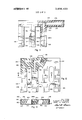
- FIG. 1 is a view of a single coaxial element, with portions cut away.
- FIG. 2 is a perspective view of a portion of an element with a Z shaped slot, and showing the phasing.
- FIG. 3 is a similar view showing the Z shaped slot transposed and the phase reversed.
- FIG. 4 is a similar view showingthe phasing of an L shaped slot.
- FIG. 5 is a further similar view showing a U shaped slot.
- FIG. 6 is a top plan view of an element with three slot configurations to show typical proportioning.
- FIG. 7 is a perspective view of a portion of a cylindrical coaxial element with a Z shaped slot.
- FIG. 8 is a perspective view of a portion of coaxial strip line.
- FIG. 9 is a perspective view showing the Z shaped slot in a collapsible antenna element.
- FIG. 10 is a perspective view of a coaxial element made by printed circuit technique.
- FIG. 11 is a top plan view, partially cut away, of an array using the structure of FIG. 10.
- FIG. 12 is a top plan view of another type of unitary array.
- FIG. 13 is a sectional view taken on line 13l3 of FIG. 12.
- the basic antenna element 10 shown in FIG. 1, comprises a tubular outer conductor 12 of rectangular cross section, with a coextensive inner conductor 14 supported therein by dielectric material 16. Part or all of the element may be enclosed in a protective plastic sheath 18 of suitable dielectric quality. At one end of the element is a coaxial feed connector 20 and at the other end is a shorting plate 22, making a complete antenna element. In one wide face of the outer conductor 12 are longitudinally spaced slots 24, which in this case are Z shaped with arms 26 extending in opposite directions parallel to the length of the element and connected by a transverse coupling portion 28.
- the inner conductor 14 is a flat metal strip of copper or the like, the outer conductor being a copper tube, which may be rigid, or in the form of plating on the dielectric material, or even a braided sheath.
- the dielectric material is Teflon, reinforced with glass cloth, but other materials may be used.
- each slot For maximum efficiency it is necessary for each slot to have a resonant impedance. This is accomplished by making the mean slot length, indicated by the broken center line 30 in FIG. 6, at least one-half wavelength of the radiation for which the antenna is designed. The amount of power radiated by the slot is determined by the area of the coupling portion 28, within the broken outline 32.
- the coupling portion is not limited to the rectangular shape shown, but it is desirable to have the medial length thereof substantially shorter than the length of arms 26, so that the majority of radiation is from the arms, in order to polarize the radiation properly.
- the instantaneous phase of the voltage across the slot 24 is represented by arrows 34, and the phase of the instantaneous radiated electrical field by arrows 36.
- the instantaneous phase of voltage across the slot is reversed, as shown by arrows 34A. This results in a phase reversal of the electrical, or E field, shown by arrows 36A.
- the phasing can be controlled in a similar manner by using an L shaped slot 38, with a single longitudinal arm 40 and a transverse coupling portion 42, as in FIG. 4.
- Arrows 44 indicate the instantaneous phase of voltage across the L shaped slot
- arrows 46 show the instantaneous phase of the E field.
- transposing the L shaped slot the phasing would be reversed in a manner similar to that shown in FIG. 3.
- the mean length 48 and coupling area 50 of the L shaped slot are indicated in FIG. 6.
- the U shaped slot 52 shown in FIGS. and 6, has a pair of adjacent parallel arms 54 and 56, coupled at one end by a transverse coupling portion 58.
- the mean length 60 includes both arms and the coupling portion and the coupling area is indicated at 62.
- the arrows 64 show the instantaneous phase of the voltage across the slot, the polarity in the two arms 54 and 56 being opposed. This provides oppositely phased E field radiation around the two arms, indicated by arrows 66 and 68.
- the resultant radiation is effectively nulled at the axis between the arms, but has broad beam width on each side.
- a Z shaped slot 70 is shown applied to a cylindrical coaxial element 72, with arms 74 extending axially and the coupling portion 76 circumferential in the outer conductor 78.
- a further configuration, shown in FIG. 8, is a strip line element 80, with a thin flat rectangular outer conductor 82 in which a Z shaped slot 84 is formed.
- any of the slot shapes may be used in any of the antenna element structures shown, and in any suitable number and spacing, according to the beam pattern and performance required. Different slot shapes may be combined in the same antenna for some purposes.
- the provision for phase reversal between adjacent slots makes it unnecessary to have the slot spacing at multiples of a half wavelength.
- the slots can be extended axially by means of the arm portions, to obtain a large radiation area with minimum transverse or circumferential extension of the slots.
- the various slot arrangements can be incorporated into antenna elements of small cross section, with efficiency comparable to much larger waveguide type structures.
- an elongated dielectric element 96 of rectangular cross section has an outer plating 98, of copper or the like, on one wide flat surface and an inner stn'p conductor 100 on the opposite surface.
- the strip conductor can be etched by conventional printed circuit methods from a plating-on the entire surface of the element 96, facilitating the manufacture from stock material plated on opposite surfaces.
- a second similar dielectric element 102 has an outer plating 104 on one flat surface and is bonded to the other dielectric element 96 by suitable low loss adhesive 106, with the strip conductor 100 sandwiched between the dielectric elements.
- the unplated sides of the assembly are covered by conductive side plates 108, or may be plated over by conventional methods to form a complete outer conductor around the element.
- the radiating slots are formed in the outer plating 104 by etching, or similar means. In this form L shaped slots and 110A are shown in transposed pairs as an example, but any other slot arrangement is applicable.
- a typical array shown in FIG. 11, has a plurality of spaced parallel radiating elements 112, 114 and 116 extending from a common feed element 118.
- Each radiating element has an inner strip conductor 120, embedded or sandwiched between two similar array shaped pieces of dielectric material 122, separated on a flat common plane of the array, similar to the basic structure of FIG. 10.
- a feed conductor 124 in feed element 118 is coupled to each inner conductor 120 in a unitary printed circuit type combination.
- the entire outer surface of the array is plated over to form an integral outer conductor 126, in a common surface of which the slots 128 and 128A are made.
- the number spacing and type of slots, and the number and spacing of the radiating elements are arranged to suit the specific beam pattern desired. With resonant slots the array will have efficient standing wave characteristics. Impedance and phase matching means can be incorporated in the feed conductor 124 as part of the basic assembly, the nature and function of such means being well known.
- FIGS. 12 and 13 A further form of multiple element array, with inherent structural strength, is shown in FIGS. 12 and 13.
- a plurality of spaced parallel inner strip conductors 130 are sandwiched between dielectric elements 132 and 134, and extend from a common feed conductor 136 with a suitable feed connection 138. Impedance transformers and other such means may be incorporated into the feed elements as necessary.
- Between and parallel to the strip conductors 130 are elongated slotted openings 140 completely through the array, the openings being separated by pillar portions 142 of the dielectric material. The structure is thus lightened, without unduly reducing the structural strength.
- the interior of each opening 140 will receive a wall plating 144, effectively forming outer conductors about the individual inner conductors 130 and making spaced radiating elements 146 within the array.
- Each radiating element has slots in a common surface, the arrangement shown utilizing Z shaped slots 148 and 148A along each element, in the outer conductor plating 150. In one element the slots have one orientation and in the next adjacent element the orientation is reversed to obtain the desired phase reversal.
- the resultant structure is light weight, rigid and, with a dielectric material such as the glass fiber reinforced Teflon mentioned, or a comparable material, is more resistant to damage than a typical thin wall waveguide assembly. While the conductive elements in FIGS. -13 are shown as having substantial thickness,
- the actual thickness will be on the order of a few thousandths of an inch, the dielectric material providing the structural support.
- a resonant slot antenna structure comprising, at least one elongated antenna element having a longitudinal inner conductor, a longitudinal outer conductor at least partially surrounding said inner conductor, supporting means for holding said inner conductor in spaced relation to and coextensive with said outer conductor, longitudinally spaced radiating slots in said outer conductor, each slot having at least one longitudinally extending arm and a transverse coupling portion at one end of the arm, said support means is a dielectric material, said slots are substantially Z shaped, with a pair of opposed arms interconnected by said coupling portions, and alternate slots have the arms thereof transposed. 2.
- a resonant slot antenna structure comprising, at least one elongated antenna element having a longitudinal inner conductor, a longitudinal outer conductor at least partially surrounding said inner conductor, supporting means for holding said inner conductor in spaced relation to and coextensive with said outer conductor, longitudinally spaced radiating slots in said outer conductor, each slot having at least one longitudinally extending arm and a transverse coupling portion at one end of the arm, said support means is a dielectric material, and said slots are substantially L shaped, with the arm thereof adjacent one side of the antenna element.
- a resonant slot antenna structure comprising,
- At least one elongated antenna element having a longitudinal inner conductor
- said support means is a dielectric material
- dielectric material is in two similar array shaped portions separated on a common flat plane of the antenna elements, said feed conductor and inner conductors comprising a unitary plated array on one of said dielectric portions.
Abstract
A resonant slot antenna composed of one or more elongated coaxial type radiating elements, each having an inner conductor supported within an outer conductor, the outer conductor having longitudinally spaced slots which are shaped to provide phase reversal between slots and spaced to avoid mutual coupling. This permits a coaxial or strip line antenna to be made with the desirable characteristics of a waveguide type. The antenna is particularly adaptable to construction by printed circuit techniques, with the slots and conductor elements etched in conductive plating on dielectric supporting material, making it possible to construct unitary arrays of multiple elements.
Description
United States Patent [151 3,696,433
Killian et al. [451 Oct. 3, 1972 [54] RESONANT SLOTANTENNA 2,511,029 6/1950 Willoughby ..343/770 X STRUCTURE Primary Examinerl-lerman Karl Saalbach [72] Invemors' g i g g fi Assistant ExaminerMarvin Nussbaum o ajon 0 o l Attorney-Carl R. Brown, Stephen L. King and Ken- [73] Assignee: Teledyne Ryan Aeronautical Comneth W. Mateer pany, San Diego, Calif. AB T ACT R [22] Filed: July 17, 1970 [57] S A resonant slot antenna composed of one or more [21 1 App! 55,848 elongated coaxial type radiating elements, each having an inner conductor supported within an outer conduc- 52 us. Cl. ..343/770, 343/771, 333/84 M tor, the quter conductor having longitudinally spaced [51] lnt. Cl. ..H0lg 13/10 slots much are Shaped to Provlde Phase reversal [58] Field of Search ..343/770, 771, 767-768 between W and P Y avid mutual P This permits a coaxial or str1p line antenna to be made 56] References Cited with the desirable characteristics of a waveguide type. The antenna is particularly adaptable to construction UNITED STATES PATENTS by printed circuit techniques, with the slots and conductor elements etched in conductive plating on Butler dielectric pp i g material i g it possible to construct unitary arrays of multiple elements. an a e 3,106,713 10/1963 Murata et a1. ..343/770 8 Claims, 13 Drawing Figures VIIIIIII'I'I'd PATENTEDnm 3 m2 SHEET 1 0F 3 INVENTORS e. KILLION ROBERTS DERLING KENT B.
ATTORNEY PATENIEDums m2 I 3.6963433 sum 2 or 3 INVENTORS DERLING G. K ON 1 KENT B. ROB S Wm M ATTORNEY PATENTEDnms 1912 3,696,433
sum 3 or s I/l8 /W ///////H .III
I% Fig. I2
INVENTORS DERLING G. KILLION KENT B. ROBERTS ATTORNEY RESONANT SLOT ANTENNA STRUCTURE BACKGROUND OF THE INVENTION Waveguide type array antennas with spaced slots have highly directional and controllable beam patterns, the spacing and phasing of the slots determining the particular radiation pattern. Slots with resonant impedance are preferable for efficiency. Slots have been incorporated in coaxial transmission lines but, since the slot should have a length of approximately one half wavelength of the radiation, circumferential slots are not practical in small sized coaxial lines. It is also difficult to obtain maximum radiation orthogonal to the axis of the antenna element due to slot phasing with circumferential slots.
SUMMARY OF THE INVENTION The antenna structure described herein has an inner conductive strip supported by a dielectric material within an outer tubular conductor, which may be of rectangular, circular, or other cross section which will support the TEM mode of the radiation. Slots are made in the outer conductor, the slots being of Z, L or U shape which causes phase reversal between slots. The slots can thus be spaced at other than multiples of the half wavelength, the effective slot length achieved by the special shaping allowing resonant slots to be incorporated in an element of small cross sectional size.
The slots of Z, L or U shape are arranged with arms extending along the length of the coaxial element and a coupling portion transverse or circumferential to the element. For maximum efficiency and to achieve a standing wave array, the mean slot length necessary for resonance is slightly greater than one-half wavelength, but may be longer. The amount of power radiated from each slot is determined by the area of the coupling portion. With the Z and L shaped slots, phase reversal is obtained by transposing the arms of adjacent slots, the U shaped slot having opposed phasing in itself.
The structure is particularly adaptable to printed circuit techniques, the slots and conductors being etched in conductive plating on dielectric substrate material, which forms the basic supporting structure of the antenna. Multiple element arrays can thus be made in unitary form in any desired configuration, with feed connections, impedance matching and phasing elements all incorporated in a printed circuit type layout. This results in a considerable reduction in cost compared to the usual assembly techniques, and permits the construction of a compact antenna without separate joints and associated fittings.
An object of this invention, therefore, is to provide a new and improved resonant slot antenna.
Another object of this invention is to provide antenna structure which enables a resonant slot configuration to be incorporated in a coaxial transmission line of small cross sectional size.
A further object of this invention is to provide a resonant slot antenna which is adapted to construction by printed circuit techniques.
Other objects and many advantages of this invention will become more apparent upon a reading of the following detailed description and an examination of the drawings, wherein like reference numerals designate like parts throughout and in which:
BRIEF DESCRIPTION OF THE DRAWINGS FIG. 1 is a view of a single coaxial element, with portions cut away.
FIG. 2 is a perspective view of a portion of an element with a Z shaped slot, and showing the phasing.
FIG. 3 is a similar view showing the Z shaped slot transposed and the phase reversed.
FIG. 4 is a similar view showingthe phasing of an L shaped slot.
FIG. 5 is a further similar view showing a U shaped slot.
FIG. 6 is a top plan view of an element with three slot configurations to show typical proportioning.
FIG. 7 is a perspective view of a portion of a cylindrical coaxial element with a Z shaped slot.
FIG. 8 is a perspective view of a portion of coaxial strip line.
FIG. 9 is a perspective view showing the Z shaped slot in a collapsible antenna element.
FIG. 10 is a perspective view of a coaxial element made by printed circuit technique.
FIG. 11 is a top plan view, partially cut away, of an array using the structure of FIG. 10.
FIG. 12 is a top plan view of another type of unitary array.
FIG. 13 is a sectional view taken on line 13l3 of FIG. 12.
DESCRIPTION OF THE PREFERRED EMBODIMENT The basic antenna element 10, shown in FIG. 1, comprises a tubular outer conductor 12 of rectangular cross section, with a coextensive inner conductor 14 supported therein by dielectric material 16. Part or all of the element may be enclosed in a protective plastic sheath 18 of suitable dielectric quality. At one end of the element is a coaxial feed connector 20 and at the other end is a shorting plate 22, making a complete antenna element. In one wide face of the outer conductor 12 are longitudinally spaced slots 24, which in this case are Z shaped with arms 26 extending in opposite directions parallel to the length of the element and connected by a transverse coupling portion 28.
As shown, the inner conductor 14 is a flat metal strip of copper or the like, the outer conductor being a copper tube, which may be rigid, or in the form of plating on the dielectric material, or even a braided sheath. One particularly suitable dielectric material is Teflon, reinforced with glass cloth, but other materials may be used.
For maximum efficiency it is necessary for each slot to have a resonant impedance. This is accomplished by making the mean slot length, indicated by the broken center line 30 in FIG. 6, at least one-half wavelength of the radiation for which the antenna is designed. The amount of power radiated by the slot is determined by the area of the coupling portion 28, within the broken outline 32. The coupling portion is not limited to the rectangular shape shown, but it is desirable to have the medial length thereof substantially shorter than the length of arms 26, so that the majority of radiation is from the arms, in order to polarize the radiation properly.
In FIG. 2, the instantaneous phase of the voltage across the slot 24 is represented by arrows 34, and the phase of the instantaneous radiated electrical field by arrows 36. By transposing the arms of the slot, as exemplified in slot 24A in FIG. 3, the instantaneous phase of voltage across the slot is reversed, as shown by arrows 34A. This results in a phase reversal of the electrical, or E field, shown by arrows 36A.
The phasing can be controlled in a similar manner by using an L shaped slot 38, with a single longitudinal arm 40 and a transverse coupling portion 42, as in FIG. 4. Arrows 44 indicate the instantaneous phase of voltage across the L shaped slot, and arrows 46 show the instantaneous phase of the E field. By transposing the L shaped slot, the phasing would be reversed in a manner similar to that shown in FIG. 3. For reference, the mean length 48 and coupling area 50 of the L shaped slot are indicated in FIG. 6.
The U shaped slot 52, shown in FIGS. and 6, has a pair of adjacent parallel arms 54 and 56, coupled at one end by a transverse coupling portion 58. The mean length 60 includes both arms and the coupling portion and the coupling area is indicated at 62. In FIG. 5, the arrows 64 show the instantaneous phase of the voltage across the slot, the polarity in the two arms 54 and 56 being opposed. This provides oppositely phased E field radiation around the two arms, indicated by arrows 66 and 68. The resultant radiation is effectively nulled at the axis between the arms, but has broad beam width on each side.
In FIG. 7, a Z shaped slot 70 is shown applied to a cylindrical coaxial element 72, with arms 74 extending axially and the coupling portion 76 circumferential in the outer conductor 78. A further configuration, shown in FIG. 8, is a strip line element 80, with a thin flat rectangular outer conductor 82 in which a Z shaped slot 84 is formed.
The waveguide type element 86, shown in FIG. 9 is fully described in copending application, Ser. No. 684,907, filed Nov. 20, 1967 and entitled An Extendable Radio Frequency Transmission Line and Antenna Structure. The cylindrical outer conductor 88 has a Z shaped slot 90, with axially extending arms 92 and a circumferential coupling portion 94.
It should be understood that any of the slot shapes may be used in any of the antenna element structures shown, and in any suitable number and spacing, according to the beam pattern and performance required. Different slot shapes may be combined in the same antenna for some purposes. In each instance, the provision for phase reversal between adjacent slots makes it unnecessary to have the slot spacing at multiples of a half wavelength. As a result the slots can be extended axially by means of the arm portions, to obtain a large radiation area with minimum transverse or circumferential extension of the slots. Thus the various slot arrangements can be incorporated into antenna elements of small cross section, with efficiency comparable to much larger waveguide type structures.
The small size in which an efficient antenna can be built, makes the structure adaptable to printed circuit techniques, a typical arrangement being shown in FIG. 10. In this structure, an elongated dielectric element 96 of rectangular cross section has an outer plating 98, of copper or the like, on one wide flat surface and an inner stn'p conductor 100 on the opposite surface. The strip conductor can be etched by conventional printed circuit methods from a plating-on the entire surface of the element 96, facilitating the manufacture from stock material plated on opposite surfaces. A second similar dielectric element 102 has an outer plating 104 on one flat surface and is bonded to the other dielectric element 96 by suitable low loss adhesive 106, with the strip conductor 100 sandwiched between the dielectric elements. The unplated sides of the assembly are covered by conductive side plates 108, or may be plated over by conventional methods to form a complete outer conductor around the element. The radiating slots are formed in the outer plating 104 by etching, or similar means. In this form L shaped slots and 110A are shown in transposed pairs as an example, but any other slot arrangement is applicable.
The printed circuit technique makes it practical to construct a unitary, multiple element array of any desired configuration, in flat form or curved to fit a supporting or surrounding surface, such as the skin of an aircraft or space vehicle. A typical array, shown in FIG. 11, has a plurality of spaced parallel radiating elements 112, 114 and 116 extending from a common feed element 118. Each radiating element has an inner strip conductor 120, embedded or sandwiched between two similar array shaped pieces of dielectric material 122, separated on a flat common plane of the array, similar to the basic structure of FIG. 10. A feed conductor 124 in feed element 118 is coupled to each inner conductor 120 in a unitary printed circuit type combination. The entire outer surface of the array is plated over to form an integral outer conductor 126, in a common surface of which the slots 128 and 128A are made. The number spacing and type of slots, and the number and spacing of the radiating elements are arranged to suit the specific beam pattern desired. With resonant slots the array will have efficient standing wave characteristics. Impedance and phase matching means can be incorporated in the feed conductor 124 as part of the basic assembly, the nature and function of such means being well known.
It should be noted that, with proper spacing of the radiating elements, two such arrays could be interfitted to form a continuous planar array.
A further form of multiple element array, with inherent structural strength, is shown in FIGS. 12 and 13. A plurality of spaced parallel inner strip conductors 130 are sandwiched between dielectric elements 132 and 134, and extend from a common feed conductor 136 with a suitable feed connection 138. Impedance transformers and other such means may be incorporated into the feed elements as necessary. Between and parallel to the strip conductors 130 are elongated slotted openings 140 completely through the array, the openings being separated by pillar portions 142 of the dielectric material. The structure is thus lightened, without unduly reducing the structural strength. When the outer surface of the array is plated over, the interior of each opening 140 will receive a wall plating 144, effectively forming outer conductors about the individual inner conductors 130 and making spaced radiating elements 146 within the array.
Each radiating element has slots in a common surface, the arrangement shown utilizing Z shaped slots 148 and 148A along each element, in the outer conductor plating 150. In one element the slots have one orientation and in the next adjacent element the orientation is reversed to obtain the desired phase reversal.
It will be evident that complex arrays can be made by low cost and established techniques and with consistent accuracy. The resultant structure is light weight, rigid and, with a dielectric material such as the glass fiber reinforced Teflon mentioned, or a comparable material, is more resistant to damage than a typical thin wall waveguide assembly. While the conductive elements in FIGS. -13 are shown as having substantial thickness,
it should be understood that the actual thickness will be on the order of a few thousandths of an inch, the dielectric material providing the structural support.
Having described our invention, we now claim: 1. A resonant slot antenna structure comprising, at least one elongated antenna element having a longitudinal inner conductor, a longitudinal outer conductor at least partially surrounding said inner conductor, supporting means for holding said inner conductor in spaced relation to and coextensive with said outer conductor, longitudinally spaced radiating slots in said outer conductor, each slot having at least one longitudinally extending arm and a transverse coupling portion at one end of the arm, said support means is a dielectric material, said slots are substantially Z shaped, with a pair of opposed arms interconnected by said coupling portions, and alternate slots have the arms thereof transposed. 2. A resonant slot antenna structure comprising, at least one elongated antenna element having a longitudinal inner conductor, a longitudinal outer conductor at least partially surrounding said inner conductor, supporting means for holding said inner conductor in spaced relation to and coextensive with said outer conductor, longitudinally spaced radiating slots in said outer conductor, each slot having at least one longitudinally extending arm and a transverse coupling portion at one end of the arm, said support means is a dielectric material, and said slots are substantially L shaped, with the arm thereof adjacent one side of the antenna element.
3. A resonant slot antenna structure comprising,
at least one elongated antenna element having a longitudinal inner conductor,
a longitudinal outer conductor at least partially surrounding said inner conductor,
supporting means for holding said inner conductor in spaced relation to and coextensive with said outer conductor,
longitudinally spaced radiating slots in said outer conductor, each slot having .at least one longitudinally extending arm and a transverse coupling portion at one end of the arm,
said support means is a dielectric material,
and a feed element having an array of antenna elements extending therefrom in spaced parallel relation, an inner feed conduc or in said feed element coupled to the inner con uctor of each antenna element, the slots in alternate antenna elements having their arms transposed relatived to the slots in adjacent antenna elements.
4. An antenna structure according to claim 2, wherein alternate slots are transposed with the arms thereof adjacent the other side of the antenna element.
5. An antenna structure according to claim 3, wherein said dielectric material is a unitary structural support in said feed element and antenna elements.
6. An antenna structure according to claim 5, wherein said outer conductor is a conductive plating on the outer surfaces of said dielectric material.
7. An antenna structure according to claim 5, wherein said dielectric material is in two similar array shaped portions separated on a common flat plane of the antenna elements, said feed conductor and inner conductors comprising a unitary plated array on one of said dielectric portions.
8. An antenna structure according to claim 3, wherein said dielectric material is a unitary structural supporting member in and between said feed element and antenna elements, said dielectric material having elongated slotted openings therethrough, between and parallel to said antenna elements, said outer conductor comprising a conductive plating on the outer surfaces of the dielectric material and on the surfaces of said slotted openings.
Claims (8)
1. A resonant slot antenna structure comprising, at least one elongated antenna element having a longitudinal inner conductor, a longitudinal outer conductor at least partially surrounding said inner conductor, supporting means for holding said inner conductor in spaced relation to and coextensive with said outer conductor, longitudinally spaced radiating slots in said outer conductor, each slot having at least one longitudinally extending arm and a transverse coupling portion at one end of the arm, said support means is a dielectric material, said slots are substantially Z shaped, with a pair of opposed arms interconnected by said coupling portions, and alternate slots have the arms thereof transposed.
2. A resonant slot antenna structure comprising, at least one elongated antenna element having a longitudinal inner conductor, a longitudinal outer conductor at least partially surrounding said inner conductor, supporting means for holding said inner conductor in spaced relation to and coextensive with said outer conductor, longitudinally spaced radiating slots in said outer conductor, each slot having at least one longitudinally extending arm and a transverse coupling portion at one end of the arm, said support means is a dielectric material, and said slots are substantially L shaped, with the arm thereof adjacent one side of the antenna element.
3. A resonant slot antenna structure comprising, at least one elongated antenna element having a longitudinal inner conductor, a longitudinal outer conductor at least partially surrounding said inner conductor, supporting means for holding said inner conductor in spaced relation to and coextensive with said outer conductor, longitudinally spaced radiating slots in said outer conductor, each slot having at least one longitudinally extending arm and a transverse coupling portion at one end of the arm, said support means is a dielectric material, and a feed element having an array of antenna elements extending therefrom in spaced parallel relation, an inner feed conductor in said feed element coupled to the inner conductor of each antenna element, the slots in alternate antenna elements having their arms transposed relatived to the slots in adjacent antenna elements.
4. An antenna structure according to claim 2, wherein alternate slots are transposed with the arms thereof adjacent the other side of the antenna element.
5. An antenna structure according to claim 3, wherein said dielectric material is a unitary structural support in said feed element and antenna elements.
6. An antenna structure according to claim 5, wherein said outer conductor is a conductive plating on the outer surfaces of said dielectric material.
7. An antenna structure according to claim 5, wherein said dielectric material is in two similar array shaped portions separated on a common flat plane of the antenna elements, said feed conductor and inner conductors comprising a unitary plated array on one of said dielectric portions.
8. An antenna structure according to claim 3, wherein said dielectric material is a unitary structural supporting member in and between said feed element and antenna elements, said dielectric material having elongated slotted openings therethrough, between and parallel to said antenna elements, said outer conductor comprising a conductive plating on the outer surfaces of the dielectric material and on the surfaces of said slotted openings.
Applications Claiming Priority (1)
| Application Number | Priority Date | Filing Date | Title |
|---|---|---|---|
| US5584870A | 1970-07-17 | 1970-07-17 |
Publications (1)
| Publication Number | Publication Date |
|---|---|
| US3696433A true US3696433A (en) | 1972-10-03 |
Family
ID=22000548
Family Applications (1)
| Application Number | Title | Priority Date | Filing Date |
|---|---|---|---|
| US55848A Expired - Lifetime US3696433A (en) | 1970-07-17 | 1970-07-17 | Resonant slot antenna structure |
Country Status (1)
| Country | Link |
|---|---|
| US (1) | US3696433A (en) |
Cited By (61)
| Publication number | Priority date | Publication date | Assignee | Title |
|---|---|---|---|---|
| US3936836A (en) * | 1974-07-25 | 1976-02-03 | Westinghouse Electric Corporation | Z slot antenna |
| US3961296A (en) * | 1975-03-06 | 1976-06-01 | Motorola, Inc. | Slotted strip-line |
| US3969730A (en) * | 1975-02-12 | 1976-07-13 | The United States Of America As Represented By The Secretary Of Transportation | Cross slot omnidirectional antenna |
| US4513291A (en) * | 1981-09-11 | 1985-04-23 | Thomson-Csf | Waveguide having radiating slots and a wide frequency band |
| US4644343A (en) * | 1985-09-30 | 1987-02-17 | The Boeing Company | Y-slot waveguide antenna element |
| US4647878A (en) * | 1984-11-14 | 1987-03-03 | Itt Corporation | Coaxial shielded directional microwave coupler |
| US4673904A (en) * | 1984-11-14 | 1987-06-16 | Itt Corporation | Micro-coaxial substrate |
| US4729510A (en) * | 1984-11-14 | 1988-03-08 | Itt Corporation | Coaxial shielded helical delay line and process |
| US4845506A (en) * | 1985-06-29 | 1989-07-04 | Nippondenso Co., Ltd. | Antenna system |
| US4916458A (en) * | 1988-02-19 | 1990-04-10 | Asahi Kasei Kogyo Kabushiki Kaisha | Slotted waveguide antenna |
| JPH0341804A (en) * | 1989-07-07 | 1991-02-22 | Shinko Seisakusho:Kk | Travelling wave feeding type coaxial slot antenna and transmission and reception system |
| US5075647A (en) * | 1990-05-16 | 1991-12-24 | Universities Research Association, Inc. | Planar slot coupled microwave hybrid |
| US5227749A (en) * | 1989-05-24 | 1993-07-13 | Alcatel Espace | Structure for making microwave circuits and components |
| US5469130A (en) * | 1992-11-27 | 1995-11-21 | Murata Mfg. Co., Ltd. | High frequency parallel strip line cable comprising connector part and connector provided on substrate for connecting with connector part thereof |
| US5546096A (en) * | 1989-09-13 | 1996-08-13 | Beam Company Limited | Traveling-wave feeder type coaxial slot antenna |
| US5596337A (en) * | 1994-02-28 | 1997-01-21 | Hazeltine Corporation | Slot array antennas |
| EP0798807A2 (en) * | 1996-03-29 | 1997-10-01 | Hitachi, Ltd. | TEM slot array antenna |
| US6172656B1 (en) * | 1999-06-29 | 2001-01-09 | Mitsubishi Denki Kabushiki Kaisha | Antenna device |
| US6445354B1 (en) * | 1999-08-16 | 2002-09-03 | Novatel, Inc. | Aperture coupled slot array antenna |
| US20040166734A1 (en) * | 2001-01-15 | 2004-08-26 | Mario Festag | Housing-shaped shielding plate for the shielding of an electrical component |
| US20050146477A1 (en) * | 2004-01-07 | 2005-07-07 | Kelly Kenneth C. | Vehicle mounted satellite antenna system with inverted L-shaped waveguide |
| US20090046025A1 (en) * | 2005-11-28 | 2009-02-19 | Peter Gardner | Antenna Arrays |
| US20100001916A1 (en) * | 2006-12-01 | 2010-01-07 | Mitsubishi Electric Corporation | Coaxial line slot array antenna and method for manufacturing the same |
| EP2169769A1 (en) * | 2008-09-30 | 2010-03-31 | Alcatel, Lucent | Radiating cable |
| US20100194500A1 (en) * | 2009-02-05 | 2010-08-05 | Fujikura Ltd. | Leaky cable |
| US8149177B1 (en) * | 2008-05-09 | 2012-04-03 | The United States Of America As Represented By The Secretary Of The Air Force | Slotted waveguide antenna stiffened structure |
| US20140118203A1 (en) * | 2012-11-01 | 2014-05-01 | John R. Sanford | Coax coupled slot antenna |
| CN104221217A (en) * | 2012-03-29 | 2014-12-17 | 三菱电机株式会社 | Waveguide slot array antenna device |
| EP2871710A1 (en) * | 2013-11-07 | 2015-05-13 | Fujitsu Limited | Antenna apparatus |
| US9172605B2 (en) | 2014-03-07 | 2015-10-27 | Ubiquiti Networks, Inc. | Cloud device identification and authentication |
| US9191037B2 (en) | 2013-10-11 | 2015-11-17 | Ubiquiti Networks, Inc. | Wireless radio system optimization by persistent spectrum analysis |
| US20160043475A1 (en) * | 2014-08-06 | 2016-02-11 | Google Inc. | Folded Radiation Slots For Short Wall Waveguide Radiation |
| US9293817B2 (en) | 2013-02-08 | 2016-03-22 | Ubiquiti Networks, Inc. | Stacked array antennas for high-speed wireless communication |
| US9325516B2 (en) | 2014-03-07 | 2016-04-26 | Ubiquiti Networks, Inc. | Power receptacle wireless access point devices for networked living and work spaces |
| US9368870B2 (en) | 2014-03-17 | 2016-06-14 | Ubiquiti Networks, Inc. | Methods of operating an access point using a plurality of directional beams |
| EP3032638A1 (en) * | 2014-12-13 | 2016-06-15 | Alcatel- Lucent Shanghai Bell Co., Ltd | Radiating cable and method of manufacturing a radiating cable |
| US9397820B2 (en) | 2013-02-04 | 2016-07-19 | Ubiquiti Networks, Inc. | Agile duplexing wireless radio devices |
| US9407010B1 (en) * | 2015-01-16 | 2016-08-02 | The United States Of America As Represented By The Secretary Of The Navy | Slotted antenna with anisotropic covering |
| US9490533B2 (en) | 2013-02-04 | 2016-11-08 | Ubiquiti Networks, Inc. | Dual receiver/transmitter radio devices with choke |
| US9496620B2 (en) | 2013-02-04 | 2016-11-15 | Ubiquiti Networks, Inc. | Radio system for long-range high-speed wireless communication |
| US9543635B2 (en) | 2013-02-04 | 2017-01-10 | Ubiquiti Networks, Inc. | Operation of radio devices for long-range high-speed wireless communication |
| US9612317B2 (en) | 2014-08-17 | 2017-04-04 | Google Inc. | Beam forming network for feeding short wall slotted waveguide arrays |
| US9653819B1 (en) | 2014-08-04 | 2017-05-16 | Waymo Llc | Waveguide antenna fabrication |
| US9766605B1 (en) | 2014-08-07 | 2017-09-19 | Waymo Llc | Methods and systems for synthesis of a waveguide array antenna |
| US9876282B1 (en) | 2015-04-02 | 2018-01-23 | Waymo Llc | Integrated lens for power and phase setting of DOEWG antenna arrays |
| US9912034B2 (en) | 2014-04-01 | 2018-03-06 | Ubiquiti Networks, Inc. | Antenna assembly |
| US20190027802A1 (en) * | 2017-07-20 | 2019-01-24 | Apple Inc. | Millimeter Wave Transmission Line Structures |
| US10651560B2 (en) * | 2013-07-25 | 2020-05-12 | Airbus Ds Gmbh | Waveguide radiator, array antenna radiator and synthetic aperture radar system |
| US20200395317A1 (en) * | 2019-06-11 | 2020-12-17 | Intel Corporation | Method for fabricating multiplexed hollow waveguides of variable type on a semiconductor package |
| US10916853B2 (en) | 2018-08-24 | 2021-02-09 | The Boeing Company | Conformal antenna with enhanced circular polarization |
| US10923831B2 (en) | 2018-08-24 | 2021-02-16 | The Boeing Company | Waveguide-fed planar antenna array with enhanced circular polarization |
| US10938082B2 (en) | 2018-08-24 | 2021-03-02 | The Boeing Company | Aperture-coupled microstrip-to-waveguide transitions |
| US10971806B2 (en) * | 2017-08-22 | 2021-04-06 | The Boeing Company | Broadband conformal antenna |
| US11177548B1 (en) | 2020-05-04 | 2021-11-16 | The Boeing Company | Electromagnetic wave concentration |
| US11199611B2 (en) * | 2018-02-20 | 2021-12-14 | Magna Electronics Inc. | Vehicle radar system with T-shaped slot antennas |
| US11233310B2 (en) | 2018-01-29 | 2022-01-25 | The Boeing Company | Low-profile conformal antenna |
| US20220285851A1 (en) * | 2019-07-12 | 2022-09-08 | Brown University | Location information from a receiver in a wireless network |
| US20220328972A1 (en) * | 2021-04-12 | 2022-10-13 | AchernarTek Inc. | Slot antenna |
| US20230146641A1 (en) * | 2017-08-25 | 2023-05-11 | Lg Electronics Inc. | Slot antenna and slot antenna array |
| TWI827258B (en) * | 2022-09-15 | 2023-12-21 | 啓碁科技股份有限公司 | Antenna structure |
| US11962281B2 (en) * | 2021-09-28 | 2024-04-16 | AchernarTek Inc. | Slot antenna |
Citations (5)
| Publication number | Priority date | Publication date | Assignee | Title |
|---|---|---|---|---|
| US2511029A (en) * | 1945-02-06 | 1950-06-13 | Int Standard Electric Corp | Dipole antenna system |
| US2761137A (en) * | 1946-01-05 | 1956-08-28 | Lester C Van Atta | Solid dielectric waveguide with metal plating |
| US2914766A (en) * | 1955-06-06 | 1959-11-24 | Sanders Associates Inc | Three conductor planar antenna |
| US3044066A (en) * | 1955-06-06 | 1962-07-10 | Sanders Associates Inc | Three conductor planar antenna |
| US3106713A (en) * | 1962-01-26 | 1963-10-08 | Furukawa Electric Co Ltd | Slot antenna having short radiating slots and long nonradiating distributed capacitance tuning slot |
-
1970
- 1970-07-17 US US55848A patent/US3696433A/en not_active Expired - Lifetime
Patent Citations (5)
| Publication number | Priority date | Publication date | Assignee | Title |
|---|---|---|---|---|
| US2511029A (en) * | 1945-02-06 | 1950-06-13 | Int Standard Electric Corp | Dipole antenna system |
| US2761137A (en) * | 1946-01-05 | 1956-08-28 | Lester C Van Atta | Solid dielectric waveguide with metal plating |
| US2914766A (en) * | 1955-06-06 | 1959-11-24 | Sanders Associates Inc | Three conductor planar antenna |
| US3044066A (en) * | 1955-06-06 | 1962-07-10 | Sanders Associates Inc | Three conductor planar antenna |
| US3106713A (en) * | 1962-01-26 | 1963-10-08 | Furukawa Electric Co Ltd | Slot antenna having short radiating slots and long nonradiating distributed capacitance tuning slot |
Cited By (94)
| Publication number | Priority date | Publication date | Assignee | Title |
|---|---|---|---|---|
| US3936836A (en) * | 1974-07-25 | 1976-02-03 | Westinghouse Electric Corporation | Z slot antenna |
| US3969730A (en) * | 1975-02-12 | 1976-07-13 | The United States Of America As Represented By The Secretary Of Transportation | Cross slot omnidirectional antenna |
| US3961296A (en) * | 1975-03-06 | 1976-06-01 | Motorola, Inc. | Slotted strip-line |
| US4513291A (en) * | 1981-09-11 | 1985-04-23 | Thomson-Csf | Waveguide having radiating slots and a wide frequency band |
| US4647878A (en) * | 1984-11-14 | 1987-03-03 | Itt Corporation | Coaxial shielded directional microwave coupler |
| US4673904A (en) * | 1984-11-14 | 1987-06-16 | Itt Corporation | Micro-coaxial substrate |
| US4729510A (en) * | 1984-11-14 | 1988-03-08 | Itt Corporation | Coaxial shielded helical delay line and process |
| US4845506A (en) * | 1985-06-29 | 1989-07-04 | Nippondenso Co., Ltd. | Antenna system |
| US4644343A (en) * | 1985-09-30 | 1987-02-17 | The Boeing Company | Y-slot waveguide antenna element |
| US4916458A (en) * | 1988-02-19 | 1990-04-10 | Asahi Kasei Kogyo Kabushiki Kaisha | Slotted waveguide antenna |
| US5227749A (en) * | 1989-05-24 | 1993-07-13 | Alcatel Espace | Structure for making microwave circuits and components |
| JPH0341804A (en) * | 1989-07-07 | 1991-02-22 | Shinko Seisakusho:Kk | Travelling wave feeding type coaxial slot antenna and transmission and reception system |
| JP2641944B2 (en) | 1989-07-07 | 1997-08-20 | 株式会社 新興製作所 | Traveling wave fed coaxial slot antenna |
| US5546096A (en) * | 1989-09-13 | 1996-08-13 | Beam Company Limited | Traveling-wave feeder type coaxial slot antenna |
| US5075647A (en) * | 1990-05-16 | 1991-12-24 | Universities Research Association, Inc. | Planar slot coupled microwave hybrid |
| US5469130A (en) * | 1992-11-27 | 1995-11-21 | Murata Mfg. Co., Ltd. | High frequency parallel strip line cable comprising connector part and connector provided on substrate for connecting with connector part thereof |
| US5596337A (en) * | 1994-02-28 | 1997-01-21 | Hazeltine Corporation | Slot array antennas |
| EP0798807A2 (en) * | 1996-03-29 | 1997-10-01 | Hitachi, Ltd. | TEM slot array antenna |
| EP0798807A3 (en) * | 1996-03-29 | 2000-04-05 | Hitachi, Ltd. | TEM slot array antenna |
| US6172656B1 (en) * | 1999-06-29 | 2001-01-09 | Mitsubishi Denki Kabushiki Kaisha | Antenna device |
| US6445354B1 (en) * | 1999-08-16 | 2002-09-03 | Novatel, Inc. | Aperture coupled slot array antenna |
| US6452560B2 (en) * | 1999-08-16 | 2002-09-17 | Novatel, Inc. | Slot array antenna with reduced edge diffraction |
| US20040166734A1 (en) * | 2001-01-15 | 2004-08-26 | Mario Festag | Housing-shaped shielding plate for the shielding of an electrical component |
| US7354311B2 (en) * | 2001-01-15 | 2008-04-08 | Finisar Corporation | Housing-shaped shielding plate for the shielding of an electrical component |
| US20050146477A1 (en) * | 2004-01-07 | 2005-07-07 | Kelly Kenneth C. | Vehicle mounted satellite antenna system with inverted L-shaped waveguide |
| US6977621B2 (en) * | 2004-01-07 | 2005-12-20 | Motia, Inc. | Vehicle mounted satellite antenna system with inverted L-shaped waveguide |
| US20090046025A1 (en) * | 2005-11-28 | 2009-02-19 | Peter Gardner | Antenna Arrays |
| US8253636B2 (en) * | 2005-11-28 | 2012-08-28 | Bae Systems Plc | Improvements relating to antenna arrays |
| US8134514B2 (en) * | 2006-12-01 | 2012-03-13 | Mitsubishi Electric Corporation | Coaxial line slot array antenna and method for manufacturing the same |
| US20100001916A1 (en) * | 2006-12-01 | 2010-01-07 | Mitsubishi Electric Corporation | Coaxial line slot array antenna and method for manufacturing the same |
| US8149177B1 (en) * | 2008-05-09 | 2012-04-03 | The United States Of America As Represented By The Secretary Of The Air Force | Slotted waveguide antenna stiffened structure |
| EP2169769A1 (en) * | 2008-09-30 | 2010-03-31 | Alcatel, Lucent | Radiating cable |
| US20100194500A1 (en) * | 2009-02-05 | 2010-08-05 | Fujikura Ltd. | Leaky cable |
| KR101130774B1 (en) * | 2009-02-05 | 2012-03-28 | 가부시키가이샤후지쿠라 | Leaky cable |
| US8384499B2 (en) * | 2009-02-05 | 2013-02-26 | Fujikura Ltd. | Leaky cable having at least one slot row for propagating electromagnetic waves that have been diffracted backwards |
| US9337546B2 (en) | 2012-03-29 | 2016-05-10 | Mitsubishi Electric Corporation | Waveguide slot array antenna device |
| CN104221217A (en) * | 2012-03-29 | 2014-12-17 | 三菱电机株式会社 | Waveguide slot array antenna device |
| CN104221217B (en) * | 2012-03-29 | 2016-08-24 | 三菱电机株式会社 | Waveguide slot array antenna apparatus |
| US20140118203A1 (en) * | 2012-11-01 | 2014-05-01 | John R. Sanford | Coax coupled slot antenna |
| CN103811875A (en) * | 2012-11-01 | 2014-05-21 | 优倍快网络公司 | Coax coupled slot antenna |
| CN103811875B (en) * | 2012-11-01 | 2016-08-17 | 优倍快网络公司 | Coaxially couple slot antenna |
| US9496620B2 (en) | 2013-02-04 | 2016-11-15 | Ubiquiti Networks, Inc. | Radio system for long-range high-speed wireless communication |
| US9543635B2 (en) | 2013-02-04 | 2017-01-10 | Ubiquiti Networks, Inc. | Operation of radio devices for long-range high-speed wireless communication |
| US9397820B2 (en) | 2013-02-04 | 2016-07-19 | Ubiquiti Networks, Inc. | Agile duplexing wireless radio devices |
| US9490533B2 (en) | 2013-02-04 | 2016-11-08 | Ubiquiti Networks, Inc. | Dual receiver/transmitter radio devices with choke |
| US9293817B2 (en) | 2013-02-08 | 2016-03-22 | Ubiquiti Networks, Inc. | Stacked array antennas for high-speed wireless communication |
| US9373885B2 (en) | 2013-02-08 | 2016-06-21 | Ubiquiti Networks, Inc. | Radio system for high-speed wireless communication |
| US9531067B2 (en) | 2013-02-08 | 2016-12-27 | Ubiquiti Networks, Inc. | Adjustable-tilt housing with flattened dome shape, array antenna, and bracket mount |
| US10651560B2 (en) * | 2013-07-25 | 2020-05-12 | Airbus Ds Gmbh | Waveguide radiator, array antenna radiator and synthetic aperture radar system |
| US9191037B2 (en) | 2013-10-11 | 2015-11-17 | Ubiquiti Networks, Inc. | Wireless radio system optimization by persistent spectrum analysis |
| EP2871710A1 (en) * | 2013-11-07 | 2015-05-13 | Fujitsu Limited | Antenna apparatus |
| US9325516B2 (en) | 2014-03-07 | 2016-04-26 | Ubiquiti Networks, Inc. | Power receptacle wireless access point devices for networked living and work spaces |
| US9172605B2 (en) | 2014-03-07 | 2015-10-27 | Ubiquiti Networks, Inc. | Cloud device identification and authentication |
| US9368870B2 (en) | 2014-03-17 | 2016-06-14 | Ubiquiti Networks, Inc. | Methods of operating an access point using a plurality of directional beams |
| US9843096B2 (en) | 2014-03-17 | 2017-12-12 | Ubiquiti Networks, Inc. | Compact radio frequency lenses |
| US9912053B2 (en) | 2014-03-17 | 2018-03-06 | Ubiquiti Networks, Inc. | Array antennas having a plurality of directional beams |
| US9941570B2 (en) | 2014-04-01 | 2018-04-10 | Ubiquiti Networks, Inc. | Compact radio frequency antenna apparatuses |
| US9912034B2 (en) | 2014-04-01 | 2018-03-06 | Ubiquiti Networks, Inc. | Antenna assembly |
| US9653819B1 (en) | 2014-08-04 | 2017-05-16 | Waymo Llc | Waveguide antenna fabrication |
| US9711870B2 (en) * | 2014-08-06 | 2017-07-18 | Waymo Llc | Folded radiation slots for short wall waveguide radiation |
| US10566701B2 (en) * | 2014-08-06 | 2020-02-18 | Waymo Llc | Folded radiation slots for short wall waveguide radiation |
| US20170279203A1 (en) * | 2014-08-06 | 2017-09-28 | Waymo Llc | Folded Radiation Slots For Short Wall Waveguide Radiation |
| CN106716718B (en) * | 2014-08-06 | 2020-11-06 | 伟摩有限责任公司 | Radiation structure and method for radiating electromagnetic energy using the same |
| US20160043475A1 (en) * | 2014-08-06 | 2016-02-11 | Google Inc. | Folded Radiation Slots For Short Wall Waveguide Radiation |
| CN106716718A (en) * | 2014-08-06 | 2017-05-24 | 谷歌公司 | Folded radiation slots for short wall waveguide radiation |
| EP3178131A4 (en) * | 2014-08-06 | 2018-10-10 | Waymo Llc | Folded radiation slots for short wall waveguide radiation |
| EP3809528A1 (en) * | 2014-08-06 | 2021-04-21 | Waymo Llc | Folded radiation slots for short wall waveguide radiation |
| JP2019057951A (en) * | 2014-08-06 | 2019-04-11 | ウェイモ エルエルシー | Folded radiation slots for short wall waveguide radiation |
| US9766605B1 (en) | 2014-08-07 | 2017-09-19 | Waymo Llc | Methods and systems for synthesis of a waveguide array antenna |
| US10394204B1 (en) | 2014-08-07 | 2019-08-27 | Waymo Llc | Methods and systems for synthesis of a waveguide array antenna |
| US9612317B2 (en) | 2014-08-17 | 2017-04-04 | Google Inc. | Beam forming network for feeding short wall slotted waveguide arrays |
| JP2019054538A (en) * | 2014-08-17 | 2019-04-04 | ウェイモ エルエルシー | Beamforming network for supplying power to short wall slotted waveguide arrays |
| EP3032638A1 (en) * | 2014-12-13 | 2016-06-15 | Alcatel- Lucent Shanghai Bell Co., Ltd | Radiating cable and method of manufacturing a radiating cable |
| US9407010B1 (en) * | 2015-01-16 | 2016-08-02 | The United States Of America As Represented By The Secretary Of The Navy | Slotted antenna with anisotropic covering |
| US9876282B1 (en) | 2015-04-02 | 2018-01-23 | Waymo Llc | Integrated lens for power and phase setting of DOEWG antenna arrays |
| US10763566B2 (en) * | 2017-07-20 | 2020-09-01 | Apple Inc. | Millimeter wave transmission line structures |
| US20190027802A1 (en) * | 2017-07-20 | 2019-01-24 | Apple Inc. | Millimeter Wave Transmission Line Structures |
| US10971806B2 (en) * | 2017-08-22 | 2021-04-06 | The Boeing Company | Broadband conformal antenna |
| US20230146641A1 (en) * | 2017-08-25 | 2023-05-11 | Lg Electronics Inc. | Slot antenna and slot antenna array |
| US11870137B2 (en) * | 2017-08-25 | 2024-01-09 | Lg Electronics Inc. | Slot antenna and slot antenna array |
| US11233310B2 (en) | 2018-01-29 | 2022-01-25 | The Boeing Company | Low-profile conformal antenna |
| US11199611B2 (en) * | 2018-02-20 | 2021-12-14 | Magna Electronics Inc. | Vehicle radar system with T-shaped slot antennas |
| US20220099793A1 (en) * | 2018-02-20 | 2022-03-31 | Magna Electronics Inc. | Vehicle radar system with t-shaped slot antennas |
| US11714164B2 (en) * | 2018-02-20 | 2023-08-01 | Magna Electronics Inc. | Vehicle radar system with t-shaped slot antennas |
| US10938082B2 (en) | 2018-08-24 | 2021-03-02 | The Boeing Company | Aperture-coupled microstrip-to-waveguide transitions |
| US10923831B2 (en) | 2018-08-24 | 2021-02-16 | The Boeing Company | Waveguide-fed planar antenna array with enhanced circular polarization |
| US10916853B2 (en) | 2018-08-24 | 2021-02-09 | The Boeing Company | Conformal antenna with enhanced circular polarization |
| US20200395317A1 (en) * | 2019-06-11 | 2020-12-17 | Intel Corporation | Method for fabricating multiplexed hollow waveguides of variable type on a semiconductor package |
| US11721650B2 (en) * | 2019-06-11 | 2023-08-08 | Intel Corporation | Method for fabricating multiplexed hollow waveguides of variable type on a semiconductor package |
| US20220285851A1 (en) * | 2019-07-12 | 2022-09-08 | Brown University | Location information from a receiver in a wireless network |
| US11177548B1 (en) | 2020-05-04 | 2021-11-16 | The Boeing Company | Electromagnetic wave concentration |
| US20220328972A1 (en) * | 2021-04-12 | 2022-10-13 | AchernarTek Inc. | Slot antenna |
| US11962281B2 (en) * | 2021-09-28 | 2024-04-16 | AchernarTek Inc. | Slot antenna |
| TWI827258B (en) * | 2022-09-15 | 2023-12-21 | 啓碁科技股份有限公司 | Antenna structure |
Similar Documents
| Publication | Publication Date | Title |
|---|---|---|
| US3696433A (en) | Resonant slot antenna structure | |
| US4125839A (en) | Dual diagonally fed electric microstrip dipole antennas | |
| US4130822A (en) | Slot antenna | |
| US4054874A (en) | Microstrip-dipole antenna elements and arrays thereof | |
| US4843403A (en) | Broadband notch antenna | |
| US5581266A (en) | Printed-circuit crossed-slot antenna | |
| CA1056942A (en) | Stripline antenna arrays | |
| EP0377858B1 (en) | Embedded surface wave antenna | |
| EP0685900B1 (en) | Antennae | |
| US4287518A (en) | Cavity-backed, micro-strip dipole antenna array | |
| US2914766A (en) | Three conductor planar antenna | |
| JPH0223702A (en) | Wide band antenna | |
| EP1493205B1 (en) | Horizontally polarized endfire antenna array | |
| US3044066A (en) | Three conductor planar antenna | |
| US3164790A (en) | Sinuously folded quarter wave stripline directional coupler | |
| GB2316233A (en) | Wide band radiating device capable of several polarizations | |
| US3286268A (en) | Log periodic antenna with parasitic elements interspersed in log periodic manner | |
| US4409595A (en) | Stripline slot array | |
| US3193831A (en) | Logarithmic periodic antenna | |
| US4528568A (en) | Slotted dipole with three layer transmission line feed | |
| US4220956A (en) | Collinear series-fed radio frequency antenna array | |
| US3039095A (en) | Broadband aircraft foil antenna | |
| US3031666A (en) | Three conductor planar antenna | |
| US2895134A (en) | Directional antenna systems | |
| US3002189A (en) | Three conductor planar antenna |