US4779037A - Dual input low dropout voltage regulator - Google Patents
Dual input low dropout voltage regulator Download PDFInfo
- Publication number
- US4779037A US4779037A US07/121,613 US12161387A US4779037A US 4779037 A US4779037 A US 4779037A US 12161387 A US12161387 A US 12161387A US 4779037 A US4779037 A US 4779037A
- Authority
- US
- United States
- Prior art keywords
- signal
- current
- input voltage
- output
- voltage
- Prior art date
- Legal status (The legal status is an assumption and is not a legal conclusion. Google has not performed a legal analysis and makes no representation as to the accuracy of the status listed.)
- Expired - Lifetime
Links
Images


Classifications
-
- G—PHYSICS
- G05—CONTROLLING; REGULATING
- G05F—SYSTEMS FOR REGULATING ELECTRIC OR MAGNETIC VARIABLES
- G05F1/00—Automatic systems in which deviations of an electric quantity from one or more predetermined values are detected at the output of the system and fed back to a device within the system to restore the detected quantity to its predetermined value or values, i.e. retroactive systems
- G05F1/10—Regulating voltage or current
- G05F1/46—Regulating voltage or current wherein the variable actually regulated by the final control device is dc
- G05F1/56—Regulating voltage or current wherein the variable actually regulated by the final control device is dc using semiconductor devices in series with the load as final control devices
- G05F1/565—Regulating voltage or current wherein the variable actually regulated by the final control device is dc using semiconductor devices in series with the load as final control devices sensing a condition of the system or its load in addition to means responsive to deviations in the output of the system, e.g. current, voltage, power factor
- G05F1/569—Regulating voltage or current wherein the variable actually regulated by the final control device is dc using semiconductor devices in series with the load as final control devices sensing a condition of the system or its load in addition to means responsive to deviations in the output of the system, e.g. current, voltage, power factor for protection
-
- H—ELECTRICITY
- H02—GENERATION; CONVERSION OR DISTRIBUTION OF ELECTRIC POWER
- H02J—CIRCUIT ARRANGEMENTS OR SYSTEMS FOR SUPPLYING OR DISTRIBUTING ELECTRIC POWER; SYSTEMS FOR STORING ELECTRIC ENERGY
- H02J9/00—Circuit arrangements for emergency or stand-by power supply, e.g. for emergency lighting
- H02J9/04—Circuit arrangements for emergency or stand-by power supply, e.g. for emergency lighting in which the distribution system is disconnected from the normal source and connected to a standby source
- H02J9/06—Circuit arrangements for emergency or stand-by power supply, e.g. for emergency lighting in which the distribution system is disconnected from the normal source and connected to a standby source with automatic change-over, e.g. UPS systems
- H02J9/061—Circuit arrangements for emergency or stand-by power supply, e.g. for emergency lighting in which the distribution system is disconnected from the normal source and connected to a standby source with automatic change-over, e.g. UPS systems for DC powered loads
Definitions
- the invention relates generally to self-switched redundant input voltage regulator circuits. More specifically, the invention relates to self-switched redundant input voltage regulator circuits having low dropout differential voltage regardless of the relative magnitude of the input voltage signals.
- an error amplifier (amplifier 1) is employed to compare a reference voltage VR (which is a 1.25 volt signal in the FIG. 1 example) with a signal proportionaly to the output voltage.
- the amplifier output controls a transistor (PNP transistor 2) through which the output current flows, by adjusting the transistor so that the output voltage (Vout) equals a fixed multiple of the reference voltage (kVR).
- a source voltage (sometimes referred to herein as an "input voltage”), which may be unregulated, is supplied to the emitter of the transistor.
- a voltage regulator may be characterized by its "dropout voltage,” which is the lowest source voltage which will allow the regulator output voltage to remain substantially constant at kVR, the above-mentioned fixed multiple of the reference voltage. If the source voltage drops below the dropout voltage, then the regulator's output voltage will decrease below kVR.
- a redundant source voltage (V IN) is supplied to the emitter of transistor 2.
- the source voltage is redundant in the sense that the source voltage is normally supplied through diode D from a battery (and hence is denoted V BAT), but if the battery fails, the source voltage supplied to transistor 2 is the time-varying voltage V c across capacitor C 1 (V c varies as capacitor C 1 discharges).
- V BAT battery
- V c varies as capacitor C 1 discharges
- the inventive voltage regulator includes two transistors that are controlled by the output of an error amplifier, and redundant input voltage sources "V BAT" and "VCC". A first one of the transistors conducts when V BAT is greater than VCC. The other transistor conducts when VCC is greater than V BAT. When V BAT and VCC have equal magnitude, both transistors conduct.
- the inventive circuit has low dropout voltage regardless of the relative magnitude of V BAT and VCC.
- V BAT is supplied by a battery
- VCC is supplied by a storage capacitor charged by the battery.
- the discharging storage capacitor thus serves as a time-varying redundant voltage source in the event of battery failure.
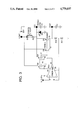
- FIG. 1 is a schematic circuit diagram of a conventional redundant input voltage regulator.
- FIG. 2 is a schematic circuit diagram of a preferred embodiment of the voltage regulator of the invention.
- FIG. 3 is a schematic circuit diagram of another preferred embodiment of the inventive voltage regulator.
- FIG. 4 is a graph of typical input and output voltage characteristics of a voltage regulator embodying the invention.
- FIG. 2 is a schematic diagram of a preferred embodiment of the invention.
- Reference voltage signsl VR is supplied to non-inverting input terminal 4 of conventional error amplifier 1.
- the base of series pass PNP transistor Q1, and the base of series pass PNP transistor Q2, are connected to the output terminal of error amplifier 1.
- Collector 10 of transistor Q1 is connected through resistor R 10 to inverting terminal 5 of amplifier 1.
- collector 11 of transistor Q2 is connected through resistor R 10 to inverting terminal 5 of amplifier 1.
- a signal (Vf) proportional to the output voltage Vout is thus fed back through resistor R 10 to inverting input terminal 5 of amplifier 1.
- Amplifier 1 compares the voltage signals supplied to input terminals 4 and 5 and generates an output signal, whose amplitude is proportional to the difference between the reference voltage VR and voltage signal Vf, for controlling the base of each of transistors Q1 and Q2.
- Output voltage terminal Vout is connected above ground by external stabilization capacitor C 2 , and resistor R 11 is connected between ground and the node labelled Vf.
- Voltage source V B is connected to bias terminal 14 of error amplifier 1 in order to provide bias current for error amplifier 1 in a conventional manner.
- V BAT will charge storage capacitor C 1 through diode D 10 until VCC equals V BAT minus the voltage drop across diode D 10 . If V BAT then decreases to below VCC (for example, if a battery associated with V BAT fails), capacitor C 1 will discharge and the associated time-varying voltage will cause transistor Q1 to remain conducting after current has ceased to flow through transistor Q2.
- the FIG. 2 circuit operates with substantially the same low dropout voltage, and with substantially the same stability regardless of the relative magnitude of VCC and V BAT, and before, during, and after a sudden decrease in the magnitude of V BAT.
- the FIG. 3 circuit shares these characteristics with the FIG. 2 circuit. Additionally, however, the FIG. 3 embodiment of the invention includes additional circuit components for the purpose of enhancing the circuit's stability in a wider range of operating modes.
- the FIG. 3 circuit includes transistors Q1 and Q2, resistors R 10 and R 11 , external storage capacitor C 1 , a source of reference voltage VR, and a source of input voltage V BAT, which are connected as are the corresponding components of the FIG. 2 circuit.
- Diode D 1 and resistor R 3 comprise a charging circuit for capacitor C 1 which corresponds to that including diode D 10 of FIG. 2.
- Zener diode D 2 is preferably connected between voltage source VCC and the emitter of transistor Q1, to permit use of a physically smaller, less expensive capacitor C 1 than would be required absent Zener diode D 2 .
- Error amplifier 6 performs the same function as that performed by amplifier 1 in the FIG. 2 circuit, but is so connected to the other circuit elements that its output drive capability, which is controlled by the magnitude of the bias current at bias terminal 14, varies in response to the error amplifier output current at output terminal 12.
- the other bias terminal 20 of error amplifier 6 is connected to ground. Error amplifier 6 has conventional design, as does error amplifier 1.
- the amount of bias current at terminal 14 of amplifier 16 is determined by the state of multiple collector PNP transistors Q3 and Q4.
- Each of transistors Q3 and Q4 is constructed in a manner well known in the art of integrated circuit fabrication.
- the emitters of transistors Q3 and Q4 are respectively connected to emitters of transistors Q2 and Q1.
- First collector 15 of transistor Q3 is connected to first collector 17 of transistor Q4 and to the base of transistor Q1 and the base of transistor Q2.
- Second collector 16 of transistor Q3 is connected to the base of transistor Q3 and to bias terminal 14 of error amplifier 6.
- Second collector 18 of transistor Q4 is connected to the base of transistor Q4 and to bias terminal 14 of error amplifier 6.
- Transistors Q3 and Q4 function as a current mirror to enhance the stability of the FIG. 3 circuit by causing the amplitude of the error amplifier bias current (at bias terminal 14) to be proportional to the amplitude of the error amplifier output current (at output terminal 12). It will be apparent from this specification to those of ordinary skill in the art how to design and construct alternative means for performing the current mirroring function performed by transistors Q3 and Q4 in FIG. 3.
- FIG. 4 Typical response curves characterizing either embodiment of the inventive circuit are set forth in FIG. 4.
- FIG. 4 assumes that storage capacitor C 1 has capacitance in the range 200 to 500 microfarads, and that VR, and resistors R 10 and R 11 are chosen so that desired output voltage (kVR) is 5 volts.
- Curve A of FIG. 4 represents input voltage V BAT
- curve B represents redundant input voltage VCC (the voltage across the storage capacitor)
- curve C represents output voltage Vout.
- V BAT and VCC are initially zero, when V BAT is increased to 12 volts, output voltage Vout will rapidly rise to 5 volts (in less than 10 msec), and VCC will rise exponentially to a level slightly less than 12 volts.
- V BAT exceeds VCC in this period, a first one of transistors Q1 and Q2 (Q1 in FIGS. 2 and 3) will be conducting during this period.
- V BAT commences a sudden decrease to zero (as shown in FIG. 4) or to a value below zero.
- the other one of transistors Q1 and Q2 (Q2 in FIGS. 2 and 3) will be conducting.
- V DO is defined as the difference between the dropout voltage (approximately 5.3 volts in the FIG. 4 example) and the desired output voltage (5 volts in the FIG. 4 example), then V DO is equal to approximately 300 mV in the FIG. 4 example.
- storage capacitance C 1 is preferably in the range 200 to 500 microfarads
- diode D 1 preferably has a reverse breakdown voltage greater than 50 volts
- resistance R3 is preferably in the range 200 to 500 ohms
- zener diode D 2 preferably has reverse breakdown voltage in the range 16 to 18 volts.
- V BAT will typically be less than 26 volts
- output capacitance C 2 will typically be on the order of 10 microfarads
- the output voltage Vout will typically be within 0.5 volts or less or a desired voltage (kVR) in the range 5.0 to 10.0 volts, with a differential dropout voltage in the range 200 mV-700 mV, provided the output current (at the Vout terminal) does not exceed a maximum of up to about 300 mA and the circuit operating temperature remains in the range from about -(40° C.) to about + 125° C.
- FIG. 2 and FIG. 3 embodiments will preferably be implemented in integrated circuit form, in a manner that will be apparent from this specification to those of ordinary skill in the art. However, these embodiments (or variations thereon) may alternatively be implemented using discrete circuit components.
Abstract
Description
Claims (14)
Priority Applications (5)
| Application Number | Priority Date | Filing Date | Title |
|---|---|---|---|
| US07/121,613 US4779037A (en) | 1987-11-17 | 1987-11-17 | Dual input low dropout voltage regulator |
| EP19880118785 EP0316781B1 (en) | 1987-11-17 | 1988-11-11 | Dual input low dropout voltage regulator |
| DE19883876388 DE3876388T2 (en) | 1987-11-17 | 1988-11-11 | VOLTAGE REGULATOR WITH TWO INPUTS WITH LOW VOLTAGE LOSS. |
| CA 583212 CA1295015C (en) | 1987-11-17 | 1988-11-16 | Dual input low drop out voltage regulator |
| JP63289002A JPH01161512A (en) | 1987-11-17 | 1988-11-17 | Dual-input low dropout voltage regulator |
Applications Claiming Priority (1)
| Application Number | Priority Date | Filing Date | Title |
|---|---|---|---|
| US07/121,613 US4779037A (en) | 1987-11-17 | 1987-11-17 | Dual input low dropout voltage regulator |
Publications (1)
| Publication Number | Publication Date |
|---|---|
| US4779037A true US4779037A (en) | 1988-10-18 |
Family
ID=22397782
Family Applications (1)
| Application Number | Title | Priority Date | Filing Date |
|---|---|---|---|
| US07/121,613 Expired - Lifetime US4779037A (en) | 1987-11-17 | 1987-11-17 | Dual input low dropout voltage regulator |
Country Status (5)
| Country | Link |
|---|---|
| US (1) | US4779037A (en) |
| EP (1) | EP0316781B1 (en) |
| JP (1) | JPH01161512A (en) |
| CA (1) | CA1295015C (en) |
| DE (1) | DE3876388T2 (en) |
Cited By (59)
| Publication number | Priority date | Publication date | Assignee | Title |
|---|---|---|---|---|
| EP0437129A2 (en) * | 1989-12-13 | 1991-07-17 | Fujitsu Limited | Card type semiconductor device |
| EP0465933A2 (en) * | 1990-07-10 | 1992-01-15 | National Semiconductor Corporation | Common emitter amplifier operating from a multiplicity of power supplies |
| US5083043A (en) * | 1990-01-18 | 1992-01-21 | Sharp Kabushiki Kaisha | Voltage control circuit for a semiconductor apparatus capable of controlling an output voltage |
| US5227714A (en) * | 1991-10-07 | 1993-07-13 | Brooktree Corporation | Voltage regulator |
| US5274323A (en) * | 1991-10-31 | 1993-12-28 | Linear Technology Corporation | Control circuit for low dropout regulator |
| US5280233A (en) * | 1991-02-27 | 1994-01-18 | Sgs-Thomson Microelectronics, S.R.L. | Low-drop voltage regulator |
| GB2277416A (en) * | 1993-04-22 | 1994-10-26 | Thames Water Utilities | Power supply; Utility meter interface |
| US5412309A (en) * | 1993-02-22 | 1995-05-02 | National Semiconductor Corporation | Current amplifiers |
| US5552697A (en) * | 1995-01-20 | 1996-09-03 | Linfinity Microelectronics | Low voltage dropout circuit with compensating capacitance circuitry |
| WO1996041248A1 (en) * | 1995-06-07 | 1996-12-19 | Analog Devices, Inc. | Frequency compensation for a low drop-out regulator |
| EP0756222A2 (en) * | 1995-07-25 | 1997-01-29 | Thomson Consumer Electronics, Inc. | Clamp circuit for remotely sensed voltage |
| US5675241A (en) * | 1995-07-06 | 1997-10-07 | Texas Instruments Incorporated | Voltage regulator with low drop out voltage |
| US5686820A (en) * | 1995-06-15 | 1997-11-11 | International Business Machines Corporation | Voltage regulator with a minimal input voltage requirement |
| EP0847124A1 (en) * | 1996-12-05 | 1998-06-10 | Alcatel | Emergency power system for providing temporary power in case of failure of a principal power source |
| US5923129A (en) * | 1997-03-14 | 1999-07-13 | Linfinity Microelectronics | Apparatus and method for starting a fluorescent lamp |
| US5930121A (en) * | 1997-03-14 | 1999-07-27 | Linfinity Microelectronics | Direct drive backlight system |
| US6002295A (en) * | 1996-10-25 | 1999-12-14 | Sgs-Thomson Microelectronics S.A. | Voltage regulator with automatic selection of a highest supply voltage |
| US6005378A (en) * | 1998-03-05 | 1999-12-21 | Impala Linear Corporation | Compact low dropout voltage regulator using enhancement and depletion mode MOS transistors |
| US6040639A (en) * | 1995-09-29 | 2000-03-21 | Telefonaktiebolaget Lm Ericsson | Circuit for improved load transient response in power supplies |
| US6097178A (en) * | 1998-09-14 | 2000-08-01 | Linear Technology Corporation | Circuits and methods for multiple-input, single-output, low-dropout voltage regulators |
| US6188212B1 (en) * | 2000-04-28 | 2001-02-13 | Burr-Brown Corporation | Low dropout voltage regulator circuit including gate offset servo circuit powered by charge pump |
| US6198266B1 (en) * | 1999-10-13 | 2001-03-06 | National Semiconductor Corporation | Low dropout voltage reference |
| US6198234B1 (en) | 1999-06-09 | 2001-03-06 | Linfinity Microelectronics | Dimmable backlight system |
| US6333623B1 (en) | 2000-10-30 | 2001-12-25 | Texas Instruments Incorporated | Complementary follower output stage circuitry and method for low dropout voltage regulator |
| US6455953B1 (en) * | 2000-02-08 | 2002-09-24 | Peter Ar-Fu Lam | Dual power modes electronics apparatus |
| US6512353B2 (en) * | 2000-07-13 | 2003-01-28 | Sipex Corporation | Synchronized, ripple independent window comparator for switch-mode power converters |
| US6614706B2 (en) * | 2000-10-13 | 2003-09-02 | Infineon Technologies Ag | Voltage regulating circuit, in particular for semiconductor memories |
| US6677735B2 (en) * | 2001-12-18 | 2004-01-13 | Texas Instruments Incorporated | Low drop-out voltage regulator having split power device |
| US20040027106A1 (en) * | 2002-08-06 | 2004-02-12 | Martins Marcus Marchesi | Soft-start system for voltage regulator and method of implementing soft-start |
| US20060113972A1 (en) * | 2004-11-29 | 2006-06-01 | Stmicroelectronics, Inc. | Low quiescent current regulator circuit |
| US20060170401A1 (en) * | 2005-02-03 | 2006-08-03 | Tien-Tzu Chen | High-efficiency linear voltage regulator |
| US20060202738A1 (en) * | 2005-03-11 | 2006-09-14 | Francesco Gatta | Line regulator with high bandwidth (BW) and high power supply rejection ratio (PSRR)and wide range of output current |
| US20070024352A1 (en) * | 2005-07-27 | 2007-02-01 | Shuyun Zhang | Distributed transistor structure for high linearity active CATV power splitter |
| US7279872B2 (en) * | 2003-08-27 | 2007-10-09 | Michael Hackner | Circuit and method for processing a supply voltage with voltage peaks |
| US20070241731A1 (en) * | 2005-06-03 | 2007-10-18 | Micrel, Incorporated | Creating Additional Phase Margin In The Open Loop Gain Of A Negative Feedback Amplifier System Using A Boost Zero Compensating Resistor |
| US7391172B2 (en) | 2003-09-23 | 2008-06-24 | Microsemi Corporation | Optical and temperature feedbacks to control display brightness |
| US7411360B2 (en) | 2002-12-13 | 2008-08-12 | Microsemi Corporation | Apparatus and method for striking a fluorescent lamp |
| US7414371B1 (en) | 2005-11-21 | 2008-08-19 | Microsemi Corporation | Voltage regulation loop with variable gain control for inverter circuit |
| US7468722B2 (en) | 2004-02-09 | 2008-12-23 | Microsemi Corporation | Method and apparatus to control display brightness with ambient light correction |
| US7525255B2 (en) | 2003-09-09 | 2009-04-28 | Microsemi Corporation | Split phase inverters for CCFL backlight system |
| US7569998B2 (en) | 2006-07-06 | 2009-08-04 | Microsemi Corporation | Striking and open lamp regulation for CCFL controller |
| US7646152B2 (en) | 2004-04-01 | 2010-01-12 | Microsemi Corporation | Full-bridge and half-bridge compatible driver timing schedule for direct drive backlight system |
| US20100156369A1 (en) * | 2008-12-18 | 2010-06-24 | Kularatna Nihal | High current voltage regulator |
| US7755595B2 (en) | 2004-06-07 | 2010-07-13 | Microsemi Corporation | Dual-slope brightness control for transflective displays |
| US20100201337A1 (en) * | 2007-05-02 | 2010-08-12 | Zetex Semiconductors Plc | Voltage regulator for low noise block |
| US20110193538A1 (en) * | 2010-02-05 | 2011-08-11 | Dialog Semiconductor Gmbh | Domino voltage regulator (dvr) |
| US8093839B2 (en) | 2008-11-20 | 2012-01-10 | Microsemi Corporation | Method and apparatus for driving CCFL at low burst duty cycle rates |
| TWI395079B (en) * | 2009-03-13 | 2013-05-01 | Advanced Analog Technology Inc | Low dropout regulator having a current-limiting mechanism |
| US8450936B1 (en) | 2010-05-13 | 2013-05-28 | Whelen Engineering Company, Inc. | Dual range power supply |
| CN103218003A (en) * | 2013-04-26 | 2013-07-24 | 无锡中星微电子有限公司 | Low-dropout voltage stabilizer with multiple power sources input |
| ITMI20120628A1 (en) * | 2012-04-17 | 2013-10-18 | Metersit S R L | STATIC GAS COUNTER WITH BATTERY ALARM SYSTEM |
| CN103441675A (en) * | 2013-08-29 | 2013-12-11 | 福尔斯通电子(昆山)有限公司 | Constant current voltage stabilizing circuit |
| CN103529894A (en) * | 2013-10-25 | 2014-01-22 | 苏州贝克微电子有限公司 | Double-input low-dropout voltage stabilizer |
| US20140062442A1 (en) * | 2012-09-05 | 2014-03-06 | Atmel Corporation | Fully integrated voltage regulator using open loop digital control for optimum power stepping and slew rate |
| CN103941798A (en) * | 2014-04-30 | 2014-07-23 | 杭州士兰微电子股份有限公司 | Low dropout regulator |
| US20140277812A1 (en) * | 2013-03-13 | 2014-09-18 | Yi-Chun Shih | Dual loop digital low drop regulator and current sharing control apparatus for distributable voltage regulators |
| IT201700035474A1 (en) * | 2017-03-31 | 2018-10-01 | St Microelectronics Srl | MATCHING VOLTAGE REGULATOR, DEVICE, EQUIPMENT AND CORRESPONDING PROCEDURE |
| US11294412B2 (en) | 2019-12-04 | 2022-04-05 | Nxp B.V. | Apparatuses and methods involving switching between dual inputs of power amplification circuitry |
| EP4250526A1 (en) * | 2022-03-24 | 2023-09-27 | FDK Corporation | Backup power supply apparatus and backup power supply apparatus controlling method |
Families Citing this family (11)
| Publication number | Priority date | Publication date | Assignee | Title |
|---|---|---|---|---|
| DE4015351A1 (en) * | 1990-05-12 | 1991-11-14 | Daimler Benz Ag | DEVICE FOR POWER SUPPLYING AN ELECTRONIC COMPUTER SYSTEM IN A MOTOR VEHICLE |
| KR19980064252A (en) * | 1996-12-19 | 1998-10-07 | 윌리엄비.켐플러 | Low Dropout Voltage Regulator with PMOS Pass Element |
| DE19710440A1 (en) * | 1997-03-13 | 1998-09-24 | Bosch Gmbh Robert | Power supply circuit |
| AT406920B (en) * | 1997-05-30 | 2000-10-25 | Siemens Ag Oesterreich | POWER SUPPLY |
| FR2807847B1 (en) * | 2000-04-12 | 2002-11-22 | St Microelectronics Sa | LINEAR REGULATOR WITH LOW OVERVOLTAGE IN TRANSIENT REGIME |
| US7402986B2 (en) | 2004-07-26 | 2008-07-22 | Wolfson Microelectronics Plc | Power supply circuit for portable battery powered device |
| GB2416605A (en) * | 2004-07-26 | 2006-02-01 | Wolfson Ltd | Dual power bus for battery powered device |
| CN102609025B (en) * | 2012-03-16 | 2013-12-11 | 电子科技大学 | Dynamic current doubling circuit and linear voltage regulator integrated with the circuit |
| KR101422924B1 (en) * | 2012-10-18 | 2014-08-13 | 삼성전기주식회사 | Low drop-out regulator |
| CN103529893A (en) * | 2013-10-18 | 2014-01-22 | 苏州贝克微电子有限公司 | Low dropout voltage stabilizer for reducing static working current |
| KR20220037280A (en) * | 2020-09-17 | 2022-03-24 | 삼성전자주식회사 | Power supply method and electronic device usint the same |
Citations (6)
| Publication number | Priority date | Publication date | Assignee | Title |
|---|---|---|---|---|
| US4209710A (en) * | 1978-06-27 | 1980-06-24 | Honeywell Inc. | Battery back-up regulator |
| US4354118A (en) * | 1981-01-30 | 1982-10-12 | Bell & Howell Company | Battery backup supply control means and method |
| US4384350A (en) * | 1980-11-03 | 1983-05-17 | Fairchild Camera & Instrument Corp. | MOS Battery backup controller for microcomputer random access memory |
| US4543522A (en) * | 1982-11-30 | 1985-09-24 | Thomson-Csf | Regulator with a low drop-out voltage |
| US4645943A (en) * | 1984-10-15 | 1987-02-24 | Dallas Semiconductor Corporation | Space-saving back-up power supply |
| US4716354A (en) * | 1985-11-12 | 1987-12-29 | Norand Corporation | Automatic voltage regulator means providing a dual low power responsive and output-voltage-controlling regulator signal particularly for a plural source battery powered system |
Family Cites Families (4)
| Publication number | Priority date | Publication date | Assignee | Title |
|---|---|---|---|---|
| JPS5512252U (en) * | 1978-07-08 | 1980-01-25 | ||
| JPS62174814A (en) * | 1986-01-28 | 1987-07-31 | Nec Ic Microcomput Syst Ltd | Stabilization power source circuit |
| US4673824A (en) * | 1986-03-03 | 1987-06-16 | Tektronix, Inc. | Power supply switch circuit |
| IT1203335B (en) * | 1987-02-23 | 1989-02-15 | Sgs Microelettronica Spa | MINIMUM VOLTAGE DROP VOLTAGE REGULATOR, SUITABLE TO SUPPORT HIGH VOLTAGE TRANSITORS |
-
1987
- 1987-11-17 US US07/121,613 patent/US4779037A/en not_active Expired - Lifetime
-
1988
- 1988-11-11 EP EP19880118785 patent/EP0316781B1/en not_active Expired - Lifetime
- 1988-11-11 DE DE19883876388 patent/DE3876388T2/en not_active Expired - Fee Related
- 1988-11-16 CA CA 583212 patent/CA1295015C/en not_active Expired - Fee Related
- 1988-11-17 JP JP63289002A patent/JPH01161512A/en active Pending
Patent Citations (6)
| Publication number | Priority date | Publication date | Assignee | Title |
|---|---|---|---|---|
| US4209710A (en) * | 1978-06-27 | 1980-06-24 | Honeywell Inc. | Battery back-up regulator |
| US4384350A (en) * | 1980-11-03 | 1983-05-17 | Fairchild Camera & Instrument Corp. | MOS Battery backup controller for microcomputer random access memory |
| US4354118A (en) * | 1981-01-30 | 1982-10-12 | Bell & Howell Company | Battery backup supply control means and method |
| US4543522A (en) * | 1982-11-30 | 1985-09-24 | Thomson-Csf | Regulator with a low drop-out voltage |
| US4645943A (en) * | 1984-10-15 | 1987-02-24 | Dallas Semiconductor Corporation | Space-saving back-up power supply |
| US4716354A (en) * | 1985-11-12 | 1987-12-29 | Norand Corporation | Automatic voltage regulator means providing a dual low power responsive and output-voltage-controlling regulator signal particularly for a plural source battery powered system |
Cited By (88)
| Publication number | Priority date | Publication date | Assignee | Title |
|---|---|---|---|---|
| EP0437129A3 (en) * | 1989-12-13 | 1992-03-18 | Fujitsu Limited | Card type semiconductor device |
| EP0437129A2 (en) * | 1989-12-13 | 1991-07-17 | Fujitsu Limited | Card type semiconductor device |
| US5083043A (en) * | 1990-01-18 | 1992-01-21 | Sharp Kabushiki Kaisha | Voltage control circuit for a semiconductor apparatus capable of controlling an output voltage |
| EP0465933A2 (en) * | 1990-07-10 | 1992-01-15 | National Semiconductor Corporation | Common emitter amplifier operating from a multiplicity of power supplies |
| US5103157A (en) * | 1990-07-10 | 1992-04-07 | National Semiconductor Corp. | Common emitter amplifiers operating from a multiplicity of power supplies |
| EP0465933A3 (en) * | 1990-07-10 | 1992-09-02 | National Semiconductor Corporation | Common emitter amplifier operating from a multiplicity of power supplies |
| US5280233A (en) * | 1991-02-27 | 1994-01-18 | Sgs-Thomson Microelectronics, S.R.L. | Low-drop voltage regulator |
| US5227714A (en) * | 1991-10-07 | 1993-07-13 | Brooktree Corporation | Voltage regulator |
| US5485109A (en) * | 1991-10-31 | 1996-01-16 | Linear Technology Corporation | Error signal generation circuit for low dropout regulators |
| US5274323A (en) * | 1991-10-31 | 1993-12-28 | Linear Technology Corporation | Control circuit for low dropout regulator |
| US5334928A (en) * | 1991-10-31 | 1994-08-02 | Linear Technology Corporation | Frequency compensation circuit for low dropout regulators |
| US5412309A (en) * | 1993-02-22 | 1995-05-02 | National Semiconductor Corporation | Current amplifiers |
| GB2277416A (en) * | 1993-04-22 | 1994-10-26 | Thames Water Utilities | Power supply; Utility meter interface |
| GB2277416B (en) * | 1993-04-22 | 1997-04-16 | Thames Water Utilities | Regulated power supply |
| US5552697A (en) * | 1995-01-20 | 1996-09-03 | Linfinity Microelectronics | Low voltage dropout circuit with compensating capacitance circuitry |
| WO1996041248A1 (en) * | 1995-06-07 | 1996-12-19 | Analog Devices, Inc. | Frequency compensation for a low drop-out regulator |
| US5631598A (en) * | 1995-06-07 | 1997-05-20 | Analog Devices, Inc. | Frequency compensation for a low drop-out regulator |
| US5686820A (en) * | 1995-06-15 | 1997-11-11 | International Business Machines Corporation | Voltage regulator with a minimal input voltage requirement |
| US5675241A (en) * | 1995-07-06 | 1997-10-07 | Texas Instruments Incorporated | Voltage regulator with low drop out voltage |
| EP0756222A2 (en) * | 1995-07-25 | 1997-01-29 | Thomson Consumer Electronics, Inc. | Clamp circuit for remotely sensed voltage |
| EP0756222A3 (en) * | 1995-07-25 | 1998-01-07 | Thomson Consumer Electronics, Inc. | Clamp circuit for remotely sensed voltage |
| US6040639A (en) * | 1995-09-29 | 2000-03-21 | Telefonaktiebolaget Lm Ericsson | Circuit for improved load transient response in power supplies |
| US6002295A (en) * | 1996-10-25 | 1999-12-14 | Sgs-Thomson Microelectronics S.A. | Voltage regulator with automatic selection of a highest supply voltage |
| US6121694A (en) * | 1996-12-05 | 2000-09-19 | Alcatel | Back-up power supply serving to compensate temporarily for main power supply deficiency |
| EP0847124A1 (en) * | 1996-12-05 | 1998-06-10 | Alcatel | Emergency power system for providing temporary power in case of failure of a principal power source |
| FR2756984A1 (en) * | 1996-12-05 | 1998-06-12 | Gec Alsthom Syst Et Serv | EMERGENCY POWER SUPPLY TEMPORARILY FOR A DEFICIENCY OF A MAIN POWER SOURCE |
| US5930121A (en) * | 1997-03-14 | 1999-07-27 | Linfinity Microelectronics | Direct drive backlight system |
| US5923129A (en) * | 1997-03-14 | 1999-07-13 | Linfinity Microelectronics | Apparatus and method for starting a fluorescent lamp |
| US6005378A (en) * | 1998-03-05 | 1999-12-21 | Impala Linear Corporation | Compact low dropout voltage regulator using enhancement and depletion mode MOS transistors |
| US6097178A (en) * | 1998-09-14 | 2000-08-01 | Linear Technology Corporation | Circuits and methods for multiple-input, single-output, low-dropout voltage regulators |
| US6198234B1 (en) | 1999-06-09 | 2001-03-06 | Linfinity Microelectronics | Dimmable backlight system |
| US6198266B1 (en) * | 1999-10-13 | 2001-03-06 | National Semiconductor Corporation | Low dropout voltage reference |
| US6455953B1 (en) * | 2000-02-08 | 2002-09-24 | Peter Ar-Fu Lam | Dual power modes electronics apparatus |
| US6188212B1 (en) * | 2000-04-28 | 2001-02-13 | Burr-Brown Corporation | Low dropout voltage regulator circuit including gate offset servo circuit powered by charge pump |
| US6512353B2 (en) * | 2000-07-13 | 2003-01-28 | Sipex Corporation | Synchronized, ripple independent window comparator for switch-mode power converters |
| US6614706B2 (en) * | 2000-10-13 | 2003-09-02 | Infineon Technologies Ag | Voltage regulating circuit, in particular for semiconductor memories |
| US6333623B1 (en) | 2000-10-30 | 2001-12-25 | Texas Instruments Incorporated | Complementary follower output stage circuitry and method for low dropout voltage regulator |
| US6677735B2 (en) * | 2001-12-18 | 2004-01-13 | Texas Instruments Incorporated | Low drop-out voltage regulator having split power device |
| US7400121B2 (en) * | 2002-08-06 | 2008-07-15 | Texas Instruments Incorporated | Soft-start system for voltage regulator and method of implementing soft-start |
| US20040027106A1 (en) * | 2002-08-06 | 2004-02-12 | Martins Marcus Marchesi | Soft-start system for voltage regulator and method of implementing soft-start |
| US7411360B2 (en) | 2002-12-13 | 2008-08-12 | Microsemi Corporation | Apparatus and method for striking a fluorescent lamp |
| US7279872B2 (en) * | 2003-08-27 | 2007-10-09 | Michael Hackner | Circuit and method for processing a supply voltage with voltage peaks |
| US7525255B2 (en) | 2003-09-09 | 2009-04-28 | Microsemi Corporation | Split phase inverters for CCFL backlight system |
| US7952298B2 (en) | 2003-09-09 | 2011-05-31 | Microsemi Corporation | Split phase inverters for CCFL backlight system |
| US7391172B2 (en) | 2003-09-23 | 2008-06-24 | Microsemi Corporation | Optical and temperature feedbacks to control display brightness |
| US8223117B2 (en) | 2004-02-09 | 2012-07-17 | Microsemi Corporation | Method and apparatus to control display brightness with ambient light correction |
| US7468722B2 (en) | 2004-02-09 | 2008-12-23 | Microsemi Corporation | Method and apparatus to control display brightness with ambient light correction |
| US7965046B2 (en) | 2004-04-01 | 2011-06-21 | Microsemi Corporation | Full-bridge and half-bridge compatible driver timing schedule for direct drive backlight system |
| US7646152B2 (en) | 2004-04-01 | 2010-01-12 | Microsemi Corporation | Full-bridge and half-bridge compatible driver timing schedule for direct drive backlight system |
| US7755595B2 (en) | 2004-06-07 | 2010-07-13 | Microsemi Corporation | Dual-slope brightness control for transflective displays |
| US7274176B2 (en) * | 2004-11-29 | 2007-09-25 | Stmicroelectronics Kk | Regulator circuit having a low quiescent current and leakage current protection |
| US20060113972A1 (en) * | 2004-11-29 | 2006-06-01 | Stmicroelectronics, Inc. | Low quiescent current regulator circuit |
| US7106032B2 (en) * | 2005-02-03 | 2006-09-12 | Aimtron Technology Corp. | Linear voltage regulator with selectable light and heavy load paths |
| US20060170401A1 (en) * | 2005-02-03 | 2006-08-03 | Tien-Tzu Chen | High-efficiency linear voltage regulator |
| US20070194812A1 (en) * | 2005-03-11 | 2007-08-23 | Francesco Gatta | Line regulator with high bandwidth (bw) and high power supply rejection ratio (psrr) and wide range of output current |
| US7212043B2 (en) * | 2005-03-11 | 2007-05-01 | Broadcom Corporation | Line regulator with high bandwidth (BW) and high power supply rejection ration (PSRR) and wide range of output current |
| US20060202738A1 (en) * | 2005-03-11 | 2006-09-14 | Francesco Gatta | Line regulator with high bandwidth (BW) and high power supply rejection ratio (PSRR)and wide range of output current |
| US7573322B2 (en) | 2005-03-11 | 2009-08-11 | Broadcom Corporation | Line regulator with high bandwidth (BW) and high power supply rejection ratio (PSRR) and wide range of output current |
| US20070241731A1 (en) * | 2005-06-03 | 2007-10-18 | Micrel, Incorporated | Creating Additional Phase Margin In The Open Loop Gain Of A Negative Feedback Amplifier System Using A Boost Zero Compensating Resistor |
| US7656139B2 (en) * | 2005-06-03 | 2010-02-02 | Micrel, Incorporated | Creating additional phase margin in the open loop gain of a negative feedback amplifier system using a boost zero compensating resistor |
| US20070024352A1 (en) * | 2005-07-27 | 2007-02-01 | Shuyun Zhang | Distributed transistor structure for high linearity active CATV power splitter |
| US7508249B2 (en) * | 2005-07-27 | 2009-03-24 | Analog Devices, Inc. | Distributed transistor structure for high linearity active CATV power splitter |
| US7414371B1 (en) | 2005-11-21 | 2008-08-19 | Microsemi Corporation | Voltage regulation loop with variable gain control for inverter circuit |
| US8358082B2 (en) | 2006-07-06 | 2013-01-22 | Microsemi Corporation | Striking and open lamp regulation for CCFL controller |
| US7569998B2 (en) | 2006-07-06 | 2009-08-04 | Microsemi Corporation | Striking and open lamp regulation for CCFL controller |
| US20100201337A1 (en) * | 2007-05-02 | 2010-08-12 | Zetex Semiconductors Plc | Voltage regulator for low noise block |
| US8093839B2 (en) | 2008-11-20 | 2012-01-10 | Microsemi Corporation | Method and apparatus for driving CCFL at low burst duty cycle rates |
| US20100156369A1 (en) * | 2008-12-18 | 2010-06-24 | Kularatna Nihal | High current voltage regulator |
| US7907430B2 (en) | 2008-12-18 | 2011-03-15 | WaikotoLink Limited | High current voltage regulator |
| TWI395079B (en) * | 2009-03-13 | 2013-05-01 | Advanced Analog Technology Inc | Low dropout regulator having a current-limiting mechanism |
| US20110193538A1 (en) * | 2010-02-05 | 2011-08-11 | Dialog Semiconductor Gmbh | Domino voltage regulator (dvr) |
| US8334681B2 (en) * | 2010-02-05 | 2012-12-18 | Dialog Semiconductor Gmbh | Domino voltage regulator (DVR) |
| US8450936B1 (en) | 2010-05-13 | 2013-05-28 | Whelen Engineering Company, Inc. | Dual range power supply |
| ITMI20120628A1 (en) * | 2012-04-17 | 2013-10-18 | Metersit S R L | STATIC GAS COUNTER WITH BATTERY ALARM SYSTEM |
| US20140062442A1 (en) * | 2012-09-05 | 2014-03-06 | Atmel Corporation | Fully integrated voltage regulator using open loop digital control for optimum power stepping and slew rate |
| US9170592B2 (en) * | 2012-09-05 | 2015-10-27 | Atmel Corporation | Fully integrated voltage regulator using open loop digital control for optimum power stepping and slew rate |
| US10698432B2 (en) * | 2013-03-13 | 2020-06-30 | Intel Corporation | Dual loop digital low drop regulator and current sharing control apparatus for distributable voltage regulators |
| US20140277812A1 (en) * | 2013-03-13 | 2014-09-18 | Yi-Chun Shih | Dual loop digital low drop regulator and current sharing control apparatus for distributable voltage regulators |
| US11921529B2 (en) | 2013-03-13 | 2024-03-05 | Intel Corporation | Dual loop digital low drop regulator and current sharing control apparatus for distributable voltage regulators |
| CN103218003A (en) * | 2013-04-26 | 2013-07-24 | 无锡中星微电子有限公司 | Low-dropout voltage stabilizer with multiple power sources input |
| CN103441675A (en) * | 2013-08-29 | 2013-12-11 | 福尔斯通电子(昆山)有限公司 | Constant current voltage stabilizing circuit |
| CN103529894A (en) * | 2013-10-25 | 2014-01-22 | 苏州贝克微电子有限公司 | Double-input low-dropout voltage stabilizer |
| CN103941798A (en) * | 2014-04-30 | 2014-07-23 | 杭州士兰微电子股份有限公司 | Low dropout regulator |
| CN103941798B (en) * | 2014-04-30 | 2015-12-02 | 杭州士兰微电子股份有限公司 | Low pressure difference linear voltage regulator |
| US10303193B2 (en) | 2017-03-31 | 2019-05-28 | Stmicroelectronics S.R.L. | Voltage regulator circuit, corresponding device, apparatus and method |
| IT201700035474A1 (en) * | 2017-03-31 | 2018-10-01 | St Microelectronics Srl | MATCHING VOLTAGE REGULATOR, DEVICE, EQUIPMENT AND CORRESPONDING PROCEDURE |
| US11294412B2 (en) | 2019-12-04 | 2022-04-05 | Nxp B.V. | Apparatuses and methods involving switching between dual inputs of power amplification circuitry |
| EP4250526A1 (en) * | 2022-03-24 | 2023-09-27 | FDK Corporation | Backup power supply apparatus and backup power supply apparatus controlling method |
Also Published As
| Publication number | Publication date |
|---|---|
| EP0316781A1 (en) | 1989-05-24 |
| DE3876388D1 (en) | 1993-01-14 |
| DE3876388T2 (en) | 1993-05-13 |
| EP0316781B1 (en) | 1992-12-02 |
| JPH01161512A (en) | 1989-06-26 |
| CA1295015C (en) | 1992-01-28 |
Similar Documents
| Publication | Publication Date | Title |
|---|---|---|
| US4779037A (en) | Dual input low dropout voltage regulator | |
| EP0862102B1 (en) | Load pole stabilized voltage regulator | |
| US5955915A (en) | Circuit for limiting the current in a power transistor | |
| US4731574A (en) | Series voltage regulator with limited current consumption at low input voltages | |
| EP0766164B1 (en) | Voltage regulator with load pole stabilization | |
| US4906913A (en) | Low dropout voltage regulator with quiescent current reduction | |
| EP0505499B1 (en) | Regulated bifurcated power supply | |
| US6177785B1 (en) | Programmable voltage regulator circuit with low power consumption feature | |
| US6806690B2 (en) | Ultra-low quiescent current low dropout (LDO) voltage regulator with dynamic bias and bandwidth | |
| US4349778A (en) | Band-gap voltage reference having an improved current mirror circuit | |
| US6208123B1 (en) | Voltage regulator with clamp circuit | |
| EP0580923A1 (en) | Circuit for detecting voltage variations in relation to a set value, for devices comprising errors amplifiers | |
| JPH1049243A (en) | Internal power circuit | |
| US4338646A (en) | Current limiting circuit | |
| US6300820B1 (en) | Voltage regulated charge pump | |
| US6091285A (en) | Constant voltage output device | |
| JPH06324092A (en) | Hysteresis circuit and power supply system having hystresis circuit | |
| US5883504A (en) | Power supply unit | |
| US4556805A (en) | Comparator circuit having hysteresis voltage substantially independent of variation in power supply voltage | |
| US5798663A (en) | Precision hysteresis generator | |
| EP0355119B1 (en) | Voltage regulator | |
| US5694031A (en) | Voltage regulator with differential current steering stage | |
| US4551691A (en) | Hysteresis circuit with small hysteresis amplitude and oscillator using the hysteresis circuit | |
| US6259287B1 (en) | Regulated voltage supply with low voltage inhibit reset circuit | |
| USRE37876E1 (en) | Power supply switch reference circuitry |
Legal Events
| Date | Code | Title | Description |
|---|---|---|---|
| AS | Assignment |
Owner name: NATIONAL SEMICONDUCTOR CORPORATION, 2900 SEMICONDU Free format text: ASSIGNMENT OF ASSIGNORS INTEREST.;ASSIGNOR:LO CASCIO, JAMES J.;REEL/FRAME:004809/0531 Effective date: 19871109 Owner name: NATIONAL SEMICONDUCTOR CORPORATION,CALIFORNIA Free format text: ASSIGNMENT OF ASSIGNORS INTEREST;ASSIGNOR:LO CASCIO, JAMES J.;REEL/FRAME:004809/0531 Effective date: 19871109 |
|
| STCF | Information on status: patent grant |
Free format text: PATENTED CASE |
|
| FEPP | Fee payment procedure |
Free format text: PAYER NUMBER DE-ASSIGNED (ORIGINAL EVENT CODE: RMPN); ENTITY STATUS OF PATENT OWNER: LARGE ENTITY Free format text: PAYOR NUMBER ASSIGNED (ORIGINAL EVENT CODE: ASPN); ENTITY STATUS OF PATENT OWNER: LARGE ENTITY |
|
| FEPP | Fee payment procedure |
Free format text: PAYOR NUMBER ASSIGNED (ORIGINAL EVENT CODE: ASPN); ENTITY STATUS OF PATENT OWNER: LARGE ENTITY |
|
| FPAY | Fee payment |
Year of fee payment: 4 |
|
| FPAY | Fee payment |
Year of fee payment: 8 |
|
| FEPP | Fee payment procedure |
Free format text: PAYER NUMBER DE-ASSIGNED (ORIGINAL EVENT CODE: RMPN); ENTITY STATUS OF PATENT OWNER: LARGE ENTITY Free format text: PAYOR NUMBER ASSIGNED (ORIGINAL EVENT CODE: ASPN); ENTITY STATUS OF PATENT OWNER: LARGE ENTITY |
|
| FPAY | Fee payment |
Year of fee payment: 12 |