US4901308A - Digital bridge for a time slot interchange digital switched matrix - Google Patents
Digital bridge for a time slot interchange digital switched matrix Download PDFInfo
- Publication number
- US4901308A US4901308A US07/343,086 US34308689A US4901308A US 4901308 A US4901308 A US 4901308A US 34308689 A US34308689 A US 34308689A US 4901308 A US4901308 A US 4901308A
- Authority
- US
- United States
- Prior art keywords
- data
- information
- ram
- output
- digital
- Prior art date
- Legal status (The legal status is an assumption and is not a legal conclusion. Google has not performed a legal analysis and makes no representation as to the accuracy of the status listed.)
- Expired - Lifetime
Links
Images


Classifications
-
- H—ELECTRICITY
- H04—ELECTRIC COMMUNICATION TECHNIQUE
- H04Q—SELECTING
- H04Q11/00—Selecting arrangements for multiplex systems
- H04Q11/04—Selecting arrangements for multiplex systems for time-division multiplexing
- H04Q11/08—Time only switching
-
- H—ELECTRICITY
- H04—ELECTRIC COMMUNICATION TECHNIQUE
- H04M—TELEPHONIC COMMUNICATION
- H04M3/00—Automatic or semi-automatic exchanges
- H04M3/42—Systems providing special services or facilities to subscribers
- H04M3/56—Arrangements for connecting several subscribers to a common circuit, i.e. affording conference facilities
- H04M3/561—Arrangements for connecting several subscribers to a common circuit, i.e. affording conference facilities by multiplexing
-
- H—ELECTRICITY
- H04—ELECTRIC COMMUNICATION TECHNIQUE
- H04M—TELEPHONIC COMMUNICATION
- H04M3/00—Automatic or semi-automatic exchanges
- H04M3/42—Systems providing special services or facilities to subscribers
- H04M3/56—Arrangements for connecting several subscribers to a common circuit, i.e. affording conference facilities
- H04M3/568—Arrangements for connecting several subscribers to a common circuit, i.e. affording conference facilities audio processing specific to telephonic conferencing, e.g. spatial distribution, mixing of participants
Definitions
- the present invention pertains in general to telephone switching matrices and, more particularly, to a switch matrix of the time slot for interchange type.
- the telephone switching matrix can be of two forms, a time matrix or a space matrix.
- a space matrix is essentially a hardwired connection whereas a time matrix involves some minimal time delay in order to provide the switching.
- One form of a time matrix is a time slot interchange (TSI) which collects data in a given transmission frame, stores the data and then outputs the data in a subsequent frame. During the subsequent frame, the data is output in a different sequence than when it was received.
- TSI time slot interchange
- the information is divided into a plurality of time domain multiplexed channels such that a predetermined number of channels exists in a given sample frame.
- Each channel consists of one sample of a linear value that is digitized and transmitted in a given time slot in the time frame.
- PCM pulse-code modulation
- a demultiplexer is typically disposed at the receiving end in the transmission system for receiving the digitized data stream and routing this information to a particular location which is a function of the time position in a particular frame. For example, if a frame were comprised of twenty-four channels the PCM information in the first channel would be routed to a first location and the information in the second channel would be routed to a second location, the remaining channels being routed to a different location also. This continues for each frame with a first location receiving the information stored in the first channel of each frame, each channel distinguished by its time slot or position in the frame. It is necessary that the first time slot in each frame receive information for only one channel in each successive frame. This is normally a straightforward task when a system is synchronized with respect to frames. However, if information is to be switched in anything other than a T1 format, there is a potential that the integrity of the channels can be altered.
- a random access memory In a conventional TSI system, information is received and sequentially stored in a random access memory (RAM) in a given frame. In the next successive frame, this information is randomly output to a different channel in a different time slot. For example, if information in channel 1 of a collection frame is received from position A and this information is to be transmitted to a position B which corresponds to the second channel in the transmission frame, it would be necessary to access the stored information in the RAM in a different sequence than it was stored such that information received in the first channel during collection is transmitted in the second channel during transmission. This therefore requires a sequential writing of data to the RAM and random reading of the data in accordance with a predetermined connection pattern. Of course, the information is delayed by a single frame.
- RAM random access memory
- the present invention overcomes the disadvantages of expanding a time matrix beyond the capabilities of the state-of-the-art access time for volatile memories to allow expansion of the system regardless of the access time of the memories.
- the present invention disclosed and claimed herein comprises a digital bridge circuit for a time slot interchange digital switch matrix.
- the digital bridge has a storage medium for receiving all of the digital call signals from the switch matrix for storage thereof to provide a collection memory.
- a conference storage device is provided for storing a conference template that defines a plurality of conferences, each conference comprised of at least two conferees.
- the digital call signals are collected during a collection frame in the collection memory and, in a subsequent accumulation frame, the digital call signals associated with the conferees in the conference are accessed in accordance with a predetermined order.
- Summation circuitry is provided for sequentially summing the accessed digital call signals for each of the conferences and storing them as a single digital conference signal for each of the conferences in an accumulation memory.
- Transmit circuitry is provided for outputting the digital conference signals to each of the associated conferees in the associated conference.
- the digital conference signal is output to the switch matrix for routing to the ports associated with the associated conferee.
- echo cancelling circuitry for subtracting the digital call signals associated with the receiving conferee from the digital conference signal.
- the digital call signal for the receiving conferee is accessed during transmission of the digital conference signal and subtracted therefrom during transmission of the digital conference signal to the receiving conferee.
- the threshold level of each of the digital call signals is accessed from the collection memory to determine if the noise exceeds a predetermined threshold. If the noise does exceed the predetermined threshold, the digital call signal is inhibited from summation with the digital call signals for the remaining conferees in the conference to reduce the level of noise in the resulting digital call conference signal.
- FIG. 1 illustrates a schematic block diagram of a general digital cross-connect system
- FIG. 2 illustrates a block schematic block diagram of a digital matrix utilizing the present invention in a time slot interchange format
- FIG. 3 illustrates a block diagram of the system of the preferred embodiment
- FIG. 4 illustrates a schematic block diagram of one of the digital matrix modules in the system of FIG. 3;
- FIG. 5 illustrates a schematic block diagram of the Multiplexer in one of the digital matrix modules in the system of FIG. 3;
- FIG. 6 illustrates a schematic block diagram of the digital matrix modules
- FIG. 7 illustrates a schematic block diagram of the memory block for page one of the memory
- FIG. 8 illustrates a schematic block diagram of the digital matrix module for the bridge function
- FIG. 9 illustrates a schematic block diagram of the bridge IC circuit.
- FIG. 1 there is illustrated a schematic block diagram of a general digital cross-connect system.
- the cross-connect system is comprised of a digital switching matrix 10 which is interfaced with individual unit sub-systems 12 labeled "1"0 through "N", the interface being an ingoing bus 14 and an outgoing bus 16 for transfer of digital information therebetween.
- Each of the unit sub-systems 12 is interfaced with DSO channels 18 on each of the unit sub-systems, each of the sub-systems 12 having a plurality of DSO channels associated therewith.
- the unit sub-systems 12 are operable to receive pulse-code modulation (PCM)information from the DSO channels and arrange this information in a channeltype format where the processing is performed by the digital switching matrix 10. This arrangement will be described in more detail hereinbelow; however, this arrangement is conventional. The information is then transmitted to the digital switching matrix 10 for storage therein and retransmission to another one of the DSO channels 18 in the cross-connect matrix. The overall operation of this system is controlled by an administrative sub-system 20.
- PCM pulse-code modulation
- Digital transmission over a voice-grade line is accomplished with a T1 carrier system.
- the signal In digitizing an analog signal for transmission along thistype of carrier system, the signal is first sampled, quantitized and then encoded. The sampling rate is around 8 kHz which results in one sample every one hundred twenty-five microseconds.
- Analog information sampling isthen encoded using pulse-code modulation (PCM) techniques, which is a common digitizing technique in use today.
- PCM pulse-code modulation
- TDM time division multiplex
- each frame there are 24 separate time slots with each slot being occupied by 8 bits, each 8 bit segment representing a PCM word representing an analog value for that particular sample of that particular channel.
- the frame therefore contains one sample for each channel plus an additional bit for frame synchronization.
- T1 carriers with T1 carrier having a transmission rate of 1.54 MBit/second with 24 PCM voice channels, the T1C carrier having a transmission rate of 3.152 MBit/S providing 48 PCM voice channels, the T2 carrier having a transmission rate of 6.312 MBit/S providing 96 PCM voice channels, the T3 carrier having a transmission rateof 44.736 MBit/S providing 672 PCM voice channels and the T4M carrier having a transmission rate of 274.176 MBit/S and providing 4032 PCM voice channels.
- T1 carrier having a transmission rate of 1.54 MBit/second with 24 PCM voice channels
- the T1C carrier having a transmission rate of 3.152 MBit/S providing 48 PCM voice channels
- the T2 carrier having a transmission rate of 6.312 MBit/S providing 96 PCM voice channels
- the T3 carrier having a transmission rateof 44.736 MBit/S providing 672 PCM voice channels
- the T4M carrier having a transmission rate of 274.176 MB
- FIG. 2 there is illustrated a schematic block diagram of a digital matrix utilizing the present invention in a time slot interchange format.
- the system is made up of a plurality of digital matrixmodules 22, each module having an input data bus 24 for receiving PCM inputdata and an output data bus 26 for outputting PCM data.
- Each of the input data buses 24 and 26 are interfaced with nodes 28 labeled "1" through "N".Each of the nodes is operable to receive information from a plurality of channels in accordance with the carrier transmission format (i.e. T1 transmission) and interface this data with the digital matrix module.
- T1 transmission the carrier transmission format
- This is a conventional format for time slot interchange.
- Each of the digital matrix modules 22 has a predetermined capacity for receiving data on the input bus 24 and outputting data on the output bus 26. This information is input to the system for storage therein and switched information is then transmitted back to one of the nodes 28 through the associated one of the output buses 26. It is the rate of retrieval of information from storage and the time constraints of the transmission format that determines the capacity of the system, since onlya finite amount of information can be input to the system for storage and retrieval. This cannot easily be cured by increasing memory because all ofthe information in a given collection frame must be accessible for output in any given time slot of a transmission frame to provide a non-blocking system.
- the T1 transmission format is utilized which provides for 24 channels.
- the 24 channels are sampled with a sampling rate8 kHz. Therefore, each frame is 125 microseconds in duration with each frame operating with a time domain multiplex (TDM) time slot of 5.2 microseconds.
- TDM time slots for the 24 channels hereinafter will be referred to as TDM time slots, t 1 -t 24 .
- each of the 24 TDM time slots, t 1 -t 24 would provide the capability of holding or allowing storage of 28 channels of information. This would result in a total of 672 channels.
- the nodes 28 determine how this information is input to the digital matrix module 22 with respect to the frame. The information would be arranged in 28 "shelves", each shelf having 24 channels corresponding to the TDM time slots t 1 -t 24 .
- the information corresponding to that time slot would be sequentially input to the bus 24 from each of the shelves such that 28 channels of information would be stored in the systemduring a given time slot and, in a similar manner, 28 channels of information would be output on bus 26 during the same time slot.
- the next 28 channels are sequentially inputfrom each of the shelves.
- Each TDM time slot requires that this transfer ofthe information from each of the 28 shelves be accomplished within 5.2 microseconds. Capacity can be expanded, of course, if more channels of information can be stored and accessed within the 5.2 microseconds. Therefore, the capacity of the system is determined by the length of the data word that must be input to or output from matrix module 22, the stored access time for reading or writing data and the duration of the TDMtime slot.
- each of the input buses 24 passes directly through the module and is connected to an intramatrix bus 30 which is a group of data buses, with one data bus in the intramatrix data bus 30 operable to receive data from only one of the digital matrix modules 22, but operable to output data to each of the digital matrix modules 22.
- a data bus 32 in the intramatrix bus 30 is interfaced with bus 24in the digital matrix module 22 associated with node #1 through a connecting bus 34.
- the data bus 32 is interfaced with the digital matrix module 22 associated with node #1 through an output bus 36, with the digital matrix module 22 associated with node #2 through an output bus 38 and with digital matrix module 22 associated with node #N through an output bus 40.
- Each of the digital matrix modules 22 has a switching RAM 42 associated therewith that has the input thereof interfaced with the intramatrix bus 30 for receiving information therefrom for a Write operation and the output thereof interfaced with the output bus 26 for a Read operation.
- a control Write circuit 44 and a control Read circuit 46 is associated with each switching RAM 42 to control the Read and Write operation.
- Each of theswitching RAMs 42 are comprised of parallel RAMs, each RAM associated with one of the data buses in the intramatrix data bus 30. This allows each of the RAMs in the switching RAM 42 to store only information received from one of the nodes. Therefore, there are N individual RAMs in each of the switching RAMs.
- the switching RAM 42 is operable to switch between the individual RAMs to select the data for output to the associated node.
- the control Read circuit 46 is operable to store a connection pattern that allows information from any channel to be transmitted to the appropriate location. However, it may be necessary to change the TDM time slot (i.e., time slot interchange) to which this information is transmitted as the receiving location may be associated with a different time slot compared to the time slot of the information when it was collected. Of course, the transmitted information may be associated with the same time slot as when it was received in a collection frame, in which case no time slot interchange is required.
- any channel information in the system that was stored in the collection frame is available for output to any given node from its associated switching RAM 42.
- the capacity of a given node 28, as described hereinabove, is determined by the number of parallel bitsthat are transmitted along output data bus 26 and the rate at which this data can be accessed from memory.
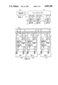
- FIG. 3 there is illustrated a block diagram of the systemof the preferred embodiment.
- the system utilizes four digital matrix modules 50, 52, 54 and 56 labeled "A" through “D”.
- Each of the digital matrix modules 50-56 are interfaced with nodes 58, 60, 62 and 64, respectively, each of the nodes 58-64 labeled "node #1-node #4", through PCM data buses 66 for inputting data to the associated module 50-56 and PCM data bus 68 for output of data from the associated one of the digital matrix modules 50-56.
- Each of the digital matrix modules 50-56 are interfaced together through an intramatrix bus 70.
- the intramatrix bus 70 is comprised of four separate buses 72, 74, 76 and 78.
- Intramatrix bus 72 is operable to transmit PCM data received from node 58 through digital matrix module 50 and disperse it to the internal switching RAM (not shown)of all of the modules.
- bus 74 is operable to receive data from node 60 through digital matrix module 52 for dispersal to all ofthe digital matrix modules 50-56
- bus 76 is operable to receive data from node 62 for dispersal to all of the digital matrix modules 50-56
- bus 78 is operable to received data from node 64 through digital matrix module56 for dispersal to all of the digital matrix modules 50-56.
- all of the intramatrix buses 72-78 are input to a digital bridge 80, the operation of which will be described hereinbelow.
- each of the digital matrix modules 50-56 receive data from the associated node and transmit it to all the modules including the module from which itoriginated for storage therein. Therefore, each of the digital matrix modules 50-56 have stored therein all of the information transmitted to the system from any of the nodes 58-64.
- extraction of data in the transmission frame is accomplished by accessing the internal switching RAM (not shown) in the associated one of the digital matrix modules 50-56 and outputting that accessed information.This is done without requiring interface with any of the digital matrix modules 50-56 in the system.
- the digital bridge 80 is utilized in a conference or broadcast mode. In this mode, information on anumber of channels is accessed from the internal switching RAM (not shown) in the digital bridge 80 and summed together for output to the other digital matrix modules 50-56 for storage therein. This allows a number of units to be combined in a single channel.
- the digital bridge 80 has one of the outputs thereof interfaced with one of the input PCM buses 66 to allow the summed data to be input back through the intramatrix bus 70 for storage in the switching RAM internal to both the digital matrix modules 50-56 and the digital bridge 80. This is done within the collection frame. During the transmission frame, this summed data is output on one of the channels and stored in the switching RAM in the digital matrix modules 50-56.
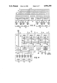
- each of the nodes 58-64 (FIG. 3) outputs 2,016 individual channels which are received from three separate subnodes in each of the nodes 58-64, each subnode outputting 672 channels.
- the separate channels utilize various multiplexing techniques to sequentially input the PCM data. This is a conventional technique.
- the nodes 58-64 are each represented by a subnode 82, a subnode 84 and a subnode 86, labeled "subnode A-subnodeC", respectively.
- the subnode 82 is interfaced with one input of a multiplexer 88 through a sixteen-bit wide data bus 90
- subnode 84 interfaced with multiplexer 88 through a sixteen-bit wide data bus 92
- subnode 86 interfaced with multiplexer 88 through a sixteen-bit wide data bus 94.
- data is received from a demultiplexer 96 and interfaced to the digital matrix module through sixteen-bit wide data buses 98, 100, and 102, respectively.
- Each of the subnodes 82 outputs 672 channels of information within a given collection frame and also receives information on the same number of channels during the transmission frame. These channels of information are organized such that 28 channels of informationare output in each of the 24 time slots t 1 -t 24 in a given frame.Therefore, there are 28 separate “shelves" of information with each shelf of information having 24 channels each with each channel on a given shelf occupying the time space of one time slot t 1 -t 24 . For all threesubnodes 82-86, 84 channels of information are output during each of the twenty-four time slots t 1 -t 24 to provide a total of 2,016 channels of information.
- All three subnodes 82-86 output three channels ofinformation at the same time with a multiplexer 88 sequentially sequencing through data presented by data buses 90-94. Therefore, in a single time slot t 1 -t 24 , the multiplexer 88 cycles twenty-eight times with twenty-eight separate channels of data presented in a sequential manner oneach of the data buses 90-94 from subnodes 82-86, respectively. In a similar manner data is output from the demultiplexer 96 to subnodes 82-86.
- the output of multiplexer 88 is connected to the bus 72 in the intramatrix bus 70 through an interconnecting bus 104, for output therefrom.
- the bus 72 is connected to the input of the switching RAM on all of the digital matrix modules 50-56.
- the output of the digital matrix modulerepresented in FIG. 4 is represented as being connected to bus 72 such thatit is input to the digital matrix modules 50-56 on bus 72 with remaining buses 74-78 being connected to the remaining three buses in the intramatrix bus 70.
- the bus 72 is input to a first bank of random access memories (RAM) comprised of a RAM 106 representing page 1 and a RAM 108 representing page0.
- RAM random access memories
- the bus 74 is connected to a second bank of RAMs with a RAM 110 representing page 1 and a RAM 112 representing page 0.
- Bus 76 is input to a third bank of RAMs represented by a RAM 114 for page 1 and a RAM 116 for page 0.
- Bus 78 is input to a fourth bank of RAMs represented by a RAM 118 for page 1 and a RAM 120 for page 0.
- Each of the RAMs 106-120 are controlled by a control RAM/Address counter 122 which is interfaced with each of the RAMs 106-120 through a control line 123.
- Each of the RAMs in each of the banks is interfaced with a bank select circuit 124 for selecting the output of one of the RAMs 106-120.
- a bank select circuit 124 for selecting the output of one of the RAMs 106-120.
- the bank select circuit 124 after selecting an appropriate output, connects one of the RAMs 106-120 to a demultiplexer 96through a line 126.
- the entire system is interfaced through an MS line and control circuitry 128 to the main system to receive signals therefrom. In addition synchronization signals are provided for system timing on lines 130.
- the system operates in a collection mode and a transmission mode.
- information is received from each of the subnodes 82-86 and this information is output on bus 104 to bus 72 and, subsequently, input to one of the RAMs in each of the digital matrix modules 50-56.
- the remaining digital matrix modules in the system output information on buses 74-78. As described above, during each time slot t 1 -t 24 , twenty-eight channels of information are collected and sequentially transmitted.
- one of the RAMs 106-120 in each bank for either page 1 or page 0 is designated as the RAM for storing collection information therein. This data is then sequentially stored in the designated RAM. For example, if page 0 is designated as being the RAM to which collected data is to be stored, information transmitted from bus 72 that is selected by multiplexer 88 is input through bus 72 to RAM 108 in digital matrix module 50. During an entire collection frame, 2,016 channels of information and twenty-eight channels for each of the twenty-four time slots (t 1 -t 24 ) are stored in the RAM 108. Therefore, the RAM 108 must be capable of accessing and storing the information at this rate. The storage rate of RAM 108 is typically one of the limiting factors of data switching.
- any storage medium Since the time within which information is to be stored in any storage medium is defined by the protocol of the system, which in this embodiment is the t 1 transmission system, more information can be processed by either utilizinga faster RAM or utilizing more complicated circuitry to buffer information for later storage. However, the latter requires more circuitry and may incur more delay between collection and transmission of data.
- the control circuit 123 in a subsequent frame redesignates the collection RAM as the page 1 RAM. Therefore, all data collected in the subsequent frame and output on bus 72is input to page 1 RAM 106.
- the RAM 108 for page 0 is designated as the output RAM. If information to be output on anyof the data buses 98-102 to subnodes 82-86 is contained in RAM 108, this information is output from RAM 108 to bank select circuit 124 and to demultiplexer 96.
- all of the page 0 RAMs 112, 116 and120 in banks 2-4 are designated as the output RAMs for transmission of datatherefrom.
- data is arranged in the RAM in a sequential manner. This is accomplished by sequentially incrementing the address in each of the RAMs designated as collection RAMs for each storage location therein. Typically, the number of storage locations will equal the maximumamount of data that can be collected and transmitted to the RAM during a given frame. For example, during the t 1 time slot, all twenty-eight channels of information output from subnodes 82-86 would be sequentially input to the RAM followed by the twenty-eight channels of information output during time slot t 2 , etc. There would therefore be twenty-eight channels of information corresponding to time slot t 1 , twenty-eight channels of information corresponding to time slot t 2 and so on for all twenty-four time slots, t 1 -t 24 .
- connection pattern is a sequence of addresses for addressing the RAMs 106-120 in a random mode that is determined by the sequence.
- control circuitry of the system controls the bank select circuit 124 to output the appropriate information.
- a remote point A transmits information to multiplexer 88 from the first of the twenty-eight channels of the time slots t 1 , it occupies the first memory location in the collection RAM.
- a remote point B may transmit information in the first of the twenty-eight channels in the second time slot t 2 . This information would be stored in the 29th storage location in the collection RAM. Therefore, remote point A would have information stored in storage location 1 and remote point B would have information stored in storage location 29.
- the storage location is a function of the sequence of transmission to the multiplexer 88. This is determined by circuitry in subnodes 82-86 and the sequence of operation of multiplexer 88.
- subnodes 82-86 operate in a similar manner to that when transmitting information to the multiplexer 88. That is, information is presented to multiplexer 88 at a predetermined rate during each time slot. During the same period of time, information can be received by that particular channel from the multiplexer 96.
- remote point A would present information to multiplexer 88 during the initial portion of time slot t 1 .
- demultiplexer 96 would also output information for transmission from the system to the remote point A.
- Subnodes 82-86 would effect the connection between remote point A and the multiplexer 88 and demultiplexer 96 of the system of FIG. 4 during that period of time. Therefore, the control RAM/Address counter 122 must first of all select the appropriate bank and the appropriate storage location during the time in which the remote pointA is receiving information from the system.
- the control RAM/Address counter 122 is addressing the first storage location corresponding to collection information of remote point A for transmission to remote point B during the time that collection information from remote point B is being stored in storage location 29 in the collection RAM.
- information is continually being stored in a sequential manner in the collection RAM and,in a subsequent frame, the collection RAM being designated a transmission RAM and the information randomly accessed in accordance with the predetermined interconnect pattern in control RAM 122 for output in a different time slot if necessary.
- the information in a given frame in the present embodiment isstored in one of 2,016 individual time slots with the bank select circuit 124 and the control RAM/Address counter 122 providing a sequence to randomly output the information in any one of the 2,016 individual time segments during the transmission mode.
- This results in only one frame of delay between the collection of data on any given channel in any time slotfor transmission of data back to the receiving one of remote points.
- all the information in this system is available in any one of the digital matrix modules. It is only necessary to store the appropriate sequence in the control RAM/Address counter 122 to associate it with the digital matrix module 50 to provide the appropriate output to the associated ones of the subnodes 82-86.
- any number of digital matrix modules can be accommodated as long as each digital matrix module has a dedicated bank of RAMs associated with that particular digital matrix module for storing a given frame of information therein.
- FIG. 5 there is illustrated a more detailed schematic block diagram of the system of FIG. 3, illustrating the multiplexer 88 in each of digital matrix modules 50-56 interconnected with three subnodes each.
- the subnodes are noted by the lower cased reference numerals a-c with the subnodes connected to digital matrix modules 50 labeled 50a, 50b and 50c.
- the four banks of RAMs are represented in general by a box labeled "switching RAM" 132.
- Each of the multiplexers 88 is connected through a parity check circuit 134 for output to the associated one of thebuses 72-78 in the intramatrix bus 70 with each of buses 72-78 interfaced with a switching RAM 132 in each of the digital matrix modules 50-56, as described above with reference to FIG. 4.
- the parity check circuits 134 are operable to check parity on the data received from the multiplexer 88 and provide an alarm signal (FIG. 4) if parity is not present.
- Each of the subnodes associated with each of the digital matrix modules 50-56 are operable to output 16-bit data at a rate of 5.376 megahertz. This data is sampled at three times that rate or at a rate of 16.128 megahertz. Therefore, 16-bit data words are output to the associated one of the buses 72-78 at a rate of 16.128 megahertz. This is the rate at which this information must be switched into the switching RAM 132 in eachof the modules 50-56.
- the capacity of the system, as described above, is limited by the rate at which a data word can be stored in the switching RAM.
- the switching RAM could store data at twice the rateof that illustrated in the present embodiment
- three additional subnodes could be added to a given digital matrix module, each outputting 16-bit data words at a rate of 5.376 megahertz and the multiplexer 88 operating at a rate of 32.256 megahertz.
- this is merely a design change anddefines the capacity of a given digital matrix module. It is important to note that the capacity of the system is a function of the way in which data can be stored during a single frame since each bank of the RAM associated with each of the digital matrix modules has a capacity which equals or exceeds the information being input to the digital matrix module. Further, by disposing in each of the digital matrix modules an associated bank of memory for each of the digital matrix modules, it is therefore possible to have local access to all the information in the system.
- information transmitted from subnode 50a is stored in each of the switching RAMs 132 and each of the digital matrix modules 50-56. If a remote point associated with subnode 54c is to receive information from subnode 50a, it is only necessary to provide a predetermined output pattern in the switching RAM 132 associated with digital matrix module 54 to effect transfer of information collected from subnode 50a and stored in switching RAM 132 in digital matrix module 54 tosubnode 54c. If information were not locally stored in each of the switching RAMs 132, it would therefore be necessary for a path to be provided between digital matrix module 54 and the storage location where the information from subnode 50a is stored and a time slot interchange performed.
- the digital bridge 80 has the four intramatrix buses 72-78 input thereto and processed through a parity/path ID check circuit 136, the output of which is input to a data RAM and bridge IC 137 for storing information andproviding a summation operation.
- the summation operation involves selectively accessing a number of channels for summation thereof into a single channel with this channel being output from the data RAM and bridgeIC on an input line 138. This line is then input to one input of the system. In the embodiment of FIG. 5 this is illustrated as the input to the input that would normally be occupied by subnode 56c with subnode 56c being disconnected from the system.
- the available number of input channels for connection to remote points would be decreased by the number of input channels occupied by subnode 56c. In the preferred embodiment, this is 672 channels.
- the line 138 therefore represents a total of 672 output channels such that the bridge circuit 80 can combine any number of the 8,064 channels stored in the data RAM in bridge IC 137 (2016 channels on each of the four intramatrix buses 72-78) for output on one of 672 channels.
- the data RAM and bridge IC 137 of the digital bridge 80 has contained therein four banks of data RAM. Each bank of RAM can hold data from 2,016 DSO channels with one data RAM associated with each of the intramatrix buses 72-78.
- the bridge IC can select up to 2016 channels from storage in the digital bridge and internal bank select circuit (not shown).
- the received channels are summed together as directed by control information from the external system processor and control circuits.
- the channels can be summed into a single output and the desired configuration for up to 672outputs.
- These outputs, described above, are input to one of the digital matrix modules 50-56 to allow cross-connection to the system from 1 to 672channels. If the maximum number of channels output by the digital bridge 80are input to one of the digital matrix modules 50-56, this results in 7392 separate channels that can be cross-connected or bridged via the digital bridge 80.
- Broadcast bridging is a situation where one input channel is broadcast (distributed) to multiple output channels.
- the source master station
- the slave stations cannot communicate with the master station or any other slave station.
- An example of this type of bridging is the transmission of stock market information from one location (master station) to brokerage houses,news services, and other subscribers (slave stations).
- the communication isone way only, from the master station to the slave stations.
- To effect broadcast bridging it is only necessary to store the information from themaster station into a given channel and control each of the connect patterns to interface the slave stations with that particular storage location that is occupied by the data from the master station.
- a split-bridge provides bidirectional channels between a single master station and multiple slave stations.
- the master station can transmit to all slave stations and receive from any slave station.
- a slave station cannot communicate with another slave station on a split-bridge.
- An example of split-bridging service is the interconnection of automatic teller machines to a central computer.
- the central computer master station
- the central computer can transmit to all of the automatic teller machines (slave stations) and receive from any of them.
- the automatic teller machine can only communicate with the central computer.
- each of the slave stations it is necessary for the transmissions from each of the slave stations to be summed in a digital bridge 80 and then output to a single channel. This single channel is then interconnected to the received input of the master station.
- the master station transmission is stored in a single storage location and the associated bank in each of the digital matrix modules 50-56 and each of the slave stations is then linked to this storage location.
- Conference bridging is where multiple channels are interconnected so that all can communicate with each other simultaneously.
- a conference bridge provides bidirectional channels between multiple locations. There is not amaster station/slave station relationship.
- An example of conference bridging service is in-house tele-conferencing where various participants at different locations are interconnected to a conference bridge. Each participant can communicate with any or all other participants.
- the transmitting station can have a feedback problem if it receives a signal comprised of the sum of all other channels and its own channel. It is desirable to cancel or significantly attenuate the receiving channel's own transmission.
- the digital bridge 80 is operable in the bridge IC 137 to sum all of the channels in the conference to provide a summed signal. The transmission from one of the receiving stations is then subtracted from the summed signal and output on one of the 672 channels on line 138 for storage in switching RAM 132 in all of the digital matrix modules 50-56.
- This channel is then interconnected with the station associated with the subtracted signal.
- a similar operation is performed such that each of the stations receives a summed signal with its own individual contribution subtracted or significantly attenuated. Therefore, during a transmission cycle, all of the summed information for each station in the conference is stored in switching RAM 132 in each of the digital matrix modules 50-56 with one storage channel being designated for transmission to the associated one of the conference stations.
- the storage location is determined by the input port to which the digital bridge 80 is interfaced.
- the connection pattern can then select the address with the aid of the bank select circuits for the appropriate storage location for output to the appropriate one of the conference stations.
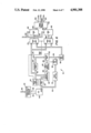
- FIG. 6 there is illustrated a schematic block diagram of the digital matrix modules 50-56. All reference numerals refer, for illustrative purposes, to digital matrix module 50.
- the digital matrix module interfaces with the administrative subsystem through a serial interface bus 140 which provides a number of control lines.
- One control line is a serial data line which is a 19.2 kBaud serial communication line.
- this serial bus is input to an administrative subsystem interface circuit 142 which provides buffering for output data to a CPU 144 on a serial line 146 and to receive data from the CPU 144 on a serial line 148.
- the CPU 144 is comprised of a microprocessor of the type HD6303RlP manufactured by Hitachi.
- This microprocessor has a serial input for receiving serial data and transmitting serial data out and converting received serial data to parallel data for transmission internally to the digital matrix module.
- Data is transmitted to the system on a processor data bus 150 which in one mode carries address information which is supplied by the administrative subsystem. These addresses are provided on a block basis such that each digital matrix module is supplied with a group of addresses for updating the internal memory, the internal memory utilized for storing the interconnect pattern.
- Control RAMs 152 are comprised of four banks of control RAMs. Each bank ofmemory is comprised of 4K bytes of memory for storing 2016 sixteen-bit datawords. Address information is received by control RAM 152 on an address bus154 and data information is written to and read out of the control RAM 152 on a data bus 156. The location to which data is to be stored in or read from is determined by the address on address bus 154 and Read/Write control information on a control line 158 which is interfaced with a Read/Write control circuit 160. Control RAM 152 is comprised of 16K of Static RAM.
- the Control RAM 152 is operable to store an interconnect pattern for the digital matrix module which essentially consists of addresses for the four banks of memory for the first and second page, as will be described hereinbelow.
- the control RAM 152 is comprised of two static random access memory (SRAM) integrated circuits of the type CY7C128 manufactured by Cypress Semiconductors. Each of these devices receives an eleven-bit address word on the address bus 154, each outputting eight bits of data to form a sixteen-bit data word.
- the control RAM 152 is fabricated from individual static RAMs that receives an eleven-bit address word on the input thereof and outputs a eight-bit data word, each page of memory in each of the banks being comprised of two 2018 data memories.
- the control RAM 152 operates in two modes, it is either written to the memory or read therefrom.
- the memory is operated in a synchronous manner such the addresses on the bus 154 are stepped through in a sequential manner.
- the addresses are generated in a modulo 2016 counter 162 which is comprised of three 74ALS163 four-bit synchronous counters which are connected in parallel to output an eleven-bit address which is initially reset at zero and then sequentially counted up to a range of 2015 by a sixteen megahertz clock.
- the output of the counter 162 is input to an address latch 164 through an address bus 166, the output of address latch 164 connected to bus 154 for providing the address information to the control RAM 152.
- the address onthe input to the control RAM 152 is sequenced through one complete cycle. In the next frame, the counter 162 is reset and the count is begun over.
- Data output from the control RAM 152 is placed onto bus 156 and then into adata out latch 168, the output of which is interfaced with the A-input of amultiplexer 170 for providing address information for page two of the memory and to the B-input of a multiplexer 172 for providing address information for page one of the memory.
- the multiplexers 170 and 172 have the remaining inputs thereof connected to the address bus 166 from the counter 162. Therefore, the multiplexers 170 and 172 are operable to receive an address from the data bus 156 or from the counter 162.
- the digital matrix module in the collection frame stores information in the switched RAM in a sequential manner and reads information from the switching RAM in a random mode in accordance with theinterconnection pattern.
- a page select signal determines whether the sequential address information is output from the multiplexers 170 or 172, this signal received on a line 174 which is interfaced with the counter 162.
- the counter 162 is comprised in part of a programmable array logic circuitand a flip-flop to distinguish between subsequent frames for both collection and transmission. This allows page one in a first frame to be the collection frame and page two the transmission frame, and in a subsequent frame controls page one to be the transmission frame and page two to be the collection frame. This alternates for all subsequent frames.
- Address comparator 182 is operable to compare the output of the counter 162 with the contents of address register 176 and output a signal on line 184 whenever there is a true comparison.
- Line 184 controls a Read/Write control circuit 160 to latch data that was stored in the temporary data register 178 into the data in latch 180 and also place the control RAM 152 in the Write mode.
- the data latched into data out latch 168 is received from the data in latch 180 andthis information is also stored in the control RAM 152 at the address that was stored in address register 176. Therefore, data to be stored in the control RAM 152 is provided by the CPU 144 and output to the switched RAM memory and also stored in the control RAM during the same time. This allows updating of control RAM 152 without requiring a separate update cycle.
- the output of multiplexer 170 is input to a block of memory 186 on a bus 188, which memory is comprised of page two of memory.
- the block of memory 190 which is interfaced with multiplexer 172 through address bus 192 comprises page one of the memory.
- Data is received from the intramatrix bus 70 on a sixteen-bit data bus 194.
- the output of memories 186 and 190 are input to a bank select/demultiplexer circuit 196 through buses 198 and200, respectively.
- Bank select/demultiplexer circuit 196 selects both the bank of memory from which data is to be output and also one of the three subnodes 50a, 50b, and 50c to which the information is to be transmitted.
- the subnodes are interfaced with the bank select/demultiplexer circuit 196through buses 202, 204 and 206. As described above, each of the buses 202 is a sixteen-bit data bus and provides 672 channels worth of information during any given frame.
- each block of memory is comprised of four banks of data, one bank for each of the digital matrix modules 50-56 in the system. If additional digital matrix modules are utilized in the system, an additional bank of memory is utilized.
- Each bank of memory is comprised of two pages, one page of whichis illustrated in FIG. 7.
- the four buses 194 that are interfaced with the intramatrix bus 70 are comprised of four individual sixteen-bit data buses208, 210, 212 and 214, which buses are interfaced with data buses 72-78 of FIG. 5.
- Data buses 208-214 are interfaced with data in latches 216, 218, 220 and 222, respectively.
- the outputs of latches 216-222 are input to page one data latches 224, 226, 228 and 230, respectively.
- data in latches 216-222 are also interfaced to page two latches (not shown) which are similar to the page one latches 224-230.
- the output of page one latches 224-230 are interfaced with intermediate data buses 232, 234, 236 and 238, respectively.
- Each of the data buses 232-238 is interfaced with the input a 32K RAM 240, 242, 244 and 246, respectively.
- Each of the 32K RAMs 240 is comprised of two 16K RAMs of the type 2018 manufactured by Toshiba Corp. for storing 2016 eight-bit words. One of the eight-bit RAMs is for storing the most significant bits and one is for storing the least significant bits.
- Data buses 232-238 are interfaced with the A-input of multiplexers 248, 250, 252 and 254, respectively.
- the remaining input of the multiplexers 248-254 is interfaced with each of the banks of page two memory block 186.
- the output of each of the multiplexers 248-254 is interfaced with bank select bus 256, which is a sixteen-bit data bus for receiving the output of one of the multiplexers 248-254.
- the multiplexers 248-254 select only from page one or page two and not from both. Therefore, information is selected from one of the RAM circuits 240-246 of page one if page one is the transmission page during the transmission frame.
- Bus 256 is interfaced with three data output latches 258, 260 and 262, the outputs of which are interfaced with buses 202, 204 and 206, respectively.
- data is first input to the data input latches 216-222 which are comprised of D-type flip-flops. The information then is either transferred to the page one latches 224-230 or similar type latches in thepage two memory block 186. These latches are also D-type flip-flops. This transfer of data occurs when the particular page is selected in the memoryto receive the data in the collection frame. In the collection mode, data is then transferred from the latches 224-230 to data buses 232-238, respectively, in the page one memory block 190.
- the Write Enable inputs ofRAMs 240-246 are controlled to store data and the page one address line 192is interfaced with the output of the counter 162 such that data is stored sequentially in the various memory locations in RAMS 240-246, as describedabove.
- buses 232-238 are unselected by multiplexers248-254, respectively.
- the latches 224-230 are inhibited from latching information onto buses 232-238, respectively.
- RAMs 240-246 are placed in the Read mode and the address bus 192 is interfaced with the output of control RAM 152 for random access to the various memories.
- Multiplexers 248-254 are then controlled to interface the selected bank with the bank select output bus 256.
- Multiplexers 248-254 are comprised of a two-to-one multiplexer for multiplexing two sixteen-bit data buses onto one sixteen-bit data bus and three-state output latches which are controlled by bank select inputs.
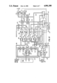
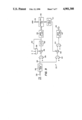
- FIG. 8 there is illustrated a schematic block diagram of the digital matrix module utilized for the bridging function.
- the digital bridge 80 utilizes four banks of RAMS similar to each of the digital matrix modules illustrated in the schematic block diagram of FIG. 6 and FIG. 7.
- the four banks of RAMs in page one are illustrated by a box 266 and the page two banks of RAM are illustrated by a box 268.
- a bidirectional bus 270 is interfaced with the data input of RAM bank 266 and also with data-in latch272 and an output data latch multiplexer 274.
- a bidirectional bus 276 is interfaced with the data port of the RAM bank 268and also with a data-in latch 278 and the data multiplexer 274.
- the buses 270 and 276 carry the PCM data, which data is stored in the RAM bank 266.
- the address input of RAM bank 266 is interfaced with a page 1 multiplexer 280 through a bus 282 and the address input on the RAM bank 268 is interfaced with a page 2 multiplexer 284 through a bus 286.
- the data-in latches 272 and 278 are both interfaced with buses 208-214, as illustratedin FIG. 7.
- the page 1 and page 2 multiplexers 280 and 284 each have two address inputs. One address input is connected through a bus 288 to a modulo 2016 counter 290 and the other input thereof connected to the output of a multiplexer 292 through a bus 294.
- the modulo 2016 counter 290 operates similar to the counter 162 in FIG. 6. In the Read mode, as described abovewith respect to the digital matrix modules, the counter 290 is operable to sequentially increment the addresses for the collection frames.
- the multiplexer 292 has two inputs, one input thereof interfaced with a bus296 and the other input thereof interfaced with a bus 298.
- the bus 296 is operable to receive data output by a control RAM 300 so the data output bythe control RAM 300 can be transferred to bus 294.
- thebus 298 is interfaced with the output of a control RAM 302. Selection of either of the control RAMS 300 or 302, in addition to selection of he appropriate bus 296 or 298, allows information stored in the control RAMs in the form of addresses to be output on bus 294 for input to the selectedone of the RAM banks 266 or 268. It should be noted that only one control RAM 300 or 302 is selected for output to bus 294.
- Buses 296 and 298 are also interfaced with data buffers 304 and 306, respectively, which have the inputs thereof interfaced with a CPU 308 through a bus 310.
- the CPU 308 has a data output thereof connected to bus 310 to allow data to be output from the CPU 308 for storage in one of the control RAMS 300 or 302.
- one of the control RAMS 300 or 302 is operable to output data in the form of addresses to the bus 294 while the other of the control RAMs 300 or 302is operable to have data stored therein for update purposes.
- the data stored in both control RAMs 300 and 302 is identical, as will be described in more detail hereinbelow.
- control RAM 300 is connected to the output of an address multiplexer 312.
- the multiplexer 312 has two inputs, one of which is connected to the bus 288 to receive the output of the counter 290 and the other input of which is connected to the address output of the CPU on a bus 314.
- the address input of the control RAM 302 is connected to the output of an address multiplexer 316.
- the address multiplexer 316 has two inputs, one of which is connected to the bus 288 and the other which is connected to the address output of the CPU 308 through the bus 314.
- the control RAMs 300 and 302 are operable similar to the control RAMS 152 of FIG.
- control RAMS 300 and 302 operate on alternate frames to output stored addresses and data from one of the RAMs 300 or 302 while updating the stored addresses and data in the other of the control RAMs 300 and 302. This is necessary sincea conference cannot be interrupted or updated on the fly.
- Each of the control RAMs is operable to store both address data and controldata.
- the control data is stored in the various fields.
- the inbound address defining the location of data to be placed in a conferenceand the outbound addresses defining the outbound time slot from the bridge 80 are stored in two separate fields, path I.D. information is stored in aseparate field, subtraction information is stored in a separate field, and an accumulator number is also stored in a separate field.
- the accumulator number represents the storage location in an internal RAM in which a conference is stored, which will be described hereinbelow.
- the entire field of data is output onto the bus 294 with the inbound address information going to the RAM banks 266 and 268.
- the addresses are stored such that the conferees ina given conference are output in a sequential manner. For example, if threeconferee's "A”, "B", and "C" were in a conference, the address locations inthe RAM banks 266 and 268 corresponding to these three conferees would be stored in adjacent memory locations such that three increments of counter 290 on the address inputs of control RAM 300 and 302 would cause the data for these three conferees to be sequentially output from RAM banks 266 or 268.
- the data output from the data latch multiplexer 274 is input to a bus 322 which is then input to one of two latch/converter circuits 324 or 326, respectively.
- the latch/converter circuits 324 and 326 are each operable on different frames to store PCM data output by the RAM banks 266 and 268.
- the latch/converter circuits 324 and 326 are operable to receive either ⁇ law Alaw data. If ⁇ law data is received, these latch/converter circuits 324 and 326 are not necessary. However, in some European countries, a different format is utilized and these circuits are necessary.
- the outputs of the latch/converter circuits 324 and 326 are interfaced withbidirectional buses 328 and 330, respectively.
- the bus 328 is input to the data input of a bridge IC 332 and the bus 330 is interfaced with the data input of a bridge IC 334.
- Each of the bridge ICs 332 and 334 have the address inputs thereof connected to a bus 336 or 338, respectively.
- the addresses determine and internal accumulator location.
- the address buses 336 and 338 are connected to the output of address latches 340 and 342, respectively.
- the inputs of latches 340 and 342 are interfaced with bus 294 to receive the accumulator address numbers which are stored in the accumulator field of the data output by the selected one of the control RAMs 300 or 302.
- the bridge ICs 332 and 334 are operable during an accumulation frame to accumulate the data for all of the conferees in a particular conference inaccordance with a predetermined accumulator number or address.
- the selected control RAM 300 or 302 would be controlled to output the inbound addresses for time slots associated with the three conferees "A", "B", and "C". Each of these locations would provide the data associated with the particular conferees which would also have associated therewith the same accumulator number.
- This accumulator number would be input to oneof the bridge ICs 332 or 334 and data on three successive cycles of accessing the banks 266 or 268 would be stored in this accumulator location internal to the selected one of the bridge ICs 332 or 334.
- data for each of the conferees is stored in one of two conference RAMs 344 and 346 at the same time that it is accumulated in the accumulating one of the bridge ICs 332 or 334.
- the information is stored in conjunction with the accumulator number defining the storage location in the accumulating one of the bridgeICs 332 or 334.
- the associated bridge IC is placed in the transmission mode and, upon transmission, the data stored inthe associated conference RAM 344 or 346 is then subtracted from the accumulated data when information is transmitted to a particular one of the conferees.
- the conference RAMs 344 and 346 have the address input thereof interfaced with conference multiplexers 348 and 350, respectively, through buses 352 and 354, respectively.
- the address data is the outbound time slot number.
- the conference multiplexers 348 and 350 each have two inputs, one input ofwhich is connected to the bus 294 and the other input of which is connectedto a modulo 672 counter 356 through a bus 358.
- the counter 356 is operable in a transmit mode to sequentially output the contents of the conference RAMs 344 or 346 in a similar manner to the operation of the counter 290.
- the counter 356 is also input to a path I.D. generator 360 which has the output thereof connected to the control input of the bridge ICs 332 and 334.
- the bus 294 is input to a control circuit 362 which receives the various control bits and the different control fields. This is interfaced on the output thereof with the bridge ICs 332 and 334.
- the bus 322 carrying the PCM data selected from the RAM banks 266 and 268 is connected to the input of a parity detect circuit 364, a path I.D. capture circuit 366 and a threshold detect circuit 368.
- the parity detect circuit has the output thereof connected to the control circuit 362 and the threshold detect circuit has the output thereof connected to the control circuit 362 also.
- the control circuit 362 is operable to control various functions of the bridge ICs 332 and 334. Additionally, the control circuits are also connected to the conference RAMS 344 and 346 to control the operation thereof with respect to Read andWrite functions.
- one of the control RAMs 300 or 302 is configured to output data under the control of the modulo 2016 counter 290.
- this data includes the inbound addresses for input to the RAM banks 266 or 268 to operate the selected one of the RAM banks in the accumulation mode.
- the other of the RAM banks 266 or 268 is in a collection mode and has the address input thereof connected to the bus 288 to receive the output of the modulo 2016 counter 290 to sequentially receive data from the associated one of the data-in latches 272 or 278 for storage therein.
- the data output by the selected one of the control RAMS 300 or 302 has the accumulator number portion thereof latched into one of the latches 340 or 342 associated with the accumulated one of the bridge ICs 332 or 334.
- the various conferees in each conference are then accumulated in the internal storage of the accumulating one of the bridge ICs 332 and 334 during the accumulating frame.
- the RAM banks 266 and 268 are alternated such that the data collected in the previous frame is now output for accumulation in the other of the bridge ICs 332 and 334.
- the one of the bridge ICs 332 and 334 that accumulated data in the previous frame is now controlled to output the conference to a predetermined one ofthe outbound time slots.
- the conference RAM 344 or 346 associated with the transmitting one of the bridge ICs 332 and 334 is alsocontrolled to output the subtraction data which is subtracted from the output conference. This provides the Echo Cancelling feature.
- the bridge ICs 332 and 334 are both connected to the input of a latch/converter circuit 370 through a bus 369 which performs the opposite conversion of the latch/converter circuits 324 and 326. This is then output to the bus 138 of FIG. 5.
- a squelch function is provided with the threshold detection circuit 368 by inhibiting storage of data from a conferee that has noise but no information. For example, if a conferee is not speaking in a conference, the power present in this conferee's signal will not exceed a certain level. If the power level exceeds a predetermined threshold, this particular conference leg is assumed to be carrying useful information andis not taken out until the power level goes back down. A delay is desired so that, for example, silence in between syllables is not taken out. The reason for squelching is to prevent the addition of large numbers of silent conferees with noise; the summed noise of all the conferees would otherwise approach the power level of an individual conferee and make participation in such a conference unpleasant.
- the threshold detect circuit 368 is input to a latch/increment circuit 372.
- the latch/incrementcircuit 372 has the input thereof connected through a bus 374 to a multiplexer circuit 376.
- the output of the latch/incrementer circuit 372 is connected through a bus 378 to the input of two statistic RAMs 380 and 382.
- the address inputs of RAMs 380 and 382 are connected to the modulo 2016 counter 290 on bus 288 with the address for the RAM 382 delayed one clock through a delay latch 384.
- the squelching operation is accomplished by comparing a factory determined number of consecutive frames of PCM data on bus 322 with detect circuit 368, with the power content of the signal below the desired squelch level,and then disabling the ability of the bridge ICs 332 and 334 to add that leg to a conference during the collection frame. One frame later, the ability to subtract it away during the output frame is also disabled. The frame that the power content goes above the squelch level, the bridge ICs are re-enabled to add the leg back into the conference. In the next frame,the leg is re-enabled for subtraction during the output frame. Once the power content goes above the squelch level, another sequence of the presetnumber of frames below the squelch level are needed before squelching is re-enabled.
- Each counter occupies a unique location within the static RAM 380 or 382.
- Each static RAM 380 has its address inputs interfaced to ten upper bits ofthe modulo 2016 counter 290 such that each squelch counter for a leg is available for two clock periods. Whenever the modulo 2016 counter 290 counts to an even value, a new squelch counter is read out of RAM 380.
- Thedata outputs of RAM 380 are interfaced to one input of a multiplexer 376, which when the modulo 2016 counter 290 is even, selects the inputs interfaced to statistic RAM 380 to be presented on the outputs.
- the outputs of the multiplexer 376 are interfaced to an increment/latch circuit 372 and to the control circuit 362.
- the control circuit 362 analyzes the state of the inputs interfaced to multiplexer 376 and if the count is at a value of 255, it disables the ability of the bridge ICs 332 and 334 to add the leg to a conference, or to subtract it on the next frame.
- the control circuit 362 and the increment/latch circuit 372 are also interfaced to the output of the threshold detect circuit 368, so thatwhen an incoming leg has a power content above the threshold level, the control circuit 362 re-enables addition of the leg into a conference and the increment/latch circuit 372 latches a factory determined count into the latch that has to be incremented up again to 255 before squelching canbe re-enabled.
- a control signal from the controlbus 294 is either:
- threshold detect circuit 368 (1) interfaced to the threshold detector 368 to indicate the leg is not to be squelched regardless of its power content, by having the threshold detect circuit 368 indicate to the control circuit 362 and the increment/latch circuit 372 that the leg is always above the squelch threshold, or
- control signal from the control bus 294 is interfaced to the control circuit 362 and to the increment/latch circuit 372, indicating that squelching is not to take place regardless of whether the threshold detect circuit 368 indicates the leg is above or below the squelch threshold.
- the increment/latch circuit 372 increments the value of the inputs interfaced to the multiplexer 376 and then latches it. If the value is at 255, it does not increment, but provides for a holding function so that the count does not wrap back around from 255 to 0.
- the latching clock is the 16 MHz clock that also drives the modulo 2016 counter 290.
- the modulo 2016 counter 290 increments next, it goes to an odd value; thus the upper ten bits of its address do not change and the same counter location in static RAM 380 is still accessed.
- the data inputs of the statistic RAM 380 are interfaced to the outputs of the increment/latch circuit 372.
- the static RAM 380 is now placed in a single Write cycle and the new value of the squelch count, stored in the increment/latch circuit 372, is written back into the static RAM 380.
- the latch delay circuit 384 delays the value of the modulo 2016 counter 290by one clock cycle, so that the static RAM 382 is one clock delayed from static RAM 380.
- static RAM 380 is being written to with the contents of the increment/latch circuit
- statistical RAM 382 whose outputs are interfaced to the input of the multiplexer 376, which is selected for outputting when the modulo 2016 counter is odd, will be presented to the inputs of the increment/latch circuit 372 and control circuit 362 for the next leg. This enables the squelch circuit to have twoclock cycles available for reading from and writing to each of the statistical RAMS 380 and 382, while providing continuous coverage of each leg.
- bridge IC 332 there is illustrated a schematic diagram of the bridge ICs 332 and 334, wherein like numerals refer to like parts in the various FIGURES.
- bridge IC 332 will be described.
- the bridge IC 334 is identical.
- the PCM data on the bus 328 is input to a ⁇ law to linear converter 390, with the output thereof input to a node 392.
- Node 392 is input to one input of a multiplexer 394, the other input of which is connected to a "O" value.
- the output of the multiplexer 394 is input to a summation circuit 396 and the other input is connected to the output of a multiplexer 398.
- the summation circuit 396 has the output thereof connected to a latch 400 to allow the data summed by the summation circuit396 to be latched.
- the output of the latch 400 is input back to one input of the multiplexer 398 on line 402.
- the multiplexer 398 has two other inputs, one input of which is connected to a "O" value and the other input which is connected to a value that alternates between a positive and a negative value of "1".
- the output of latch 400 is also connected to a linear to ⁇ law converter 404 which converts the linear value to the ⁇ law value, which value is input to the data input of an accumulator RAM 406.
- the accumulator RAM 406 providesthe internal storage locations for storing accumulated data representing conferences in accordance with the address received on the address bus 336.
- the circuit described up to the present point allows data to be input to the summation circuit 396, latched in the output data latch 400 and then fed back around to be summed with the next sequential value of the PCM data.
- the data associated with conferee "A” would first be received and latched into latch 400 and input back into thesecond input of the summation circuit 396.
- the data for conferee "B” would be presented to the input of the summation circuitry 396 and summed with the information for conferee "A", resulting in an accumulated value "A+B".
- the data corresponding to conferee "C" will be summed with the accumulated value resulting in a new accumulated value "A+B+C".
- This value will then be stored in the accumulator RAM 406 in accordance with the accumulator address on bus 336.
- a new accumulator address would then be presented to the accumulator RAM 406, and then new data for a new conference input to the bridge IC 332. It should be understood that this all occurs in a single accumulation frame.
- the bridge IC 332 After data for the various conferences are stored in the accumulator RAM 406, the bridge IC 332 is placed in the transmission mode. In this mode, the modulo 672 counter 356 illustrated in FIG. 8 will then be connected tothe address input of the conference RAM 344 which will then sequentially output both an accumulator address and subtraction data. As described above, the data was arranged in the conference RAM 344 in accordance with the outbound addresses which were generated by the control RAM 300 or 302 during the accumulation frame. In addition, the accumulator number or addresses are also stored in association with the data at each of the associated address locations in the conference RAM 344. During the transmission frame, each time that data is output in a particular time slot, it is possible to subtract the data of the conferee associated with that time slot.
- the subtraction circuitry utilizes a subtraction circuit 408 which has a minus input connected to the output of a multiplexer 410.
- Multiplexer 410 has two inputs, one input of which is connected to the node 392 to receivethe converted PCM data and the other input thereof which is connected to a "O" value.
- the positive input of the subtraction circuit 408 is connected to the output of a ⁇ law to linear conversion circuit 412 which has theinput thereof connected to the output of the accumulator RAM 406.
- the output of the subtraction circuit 408 is connected to one input of a multiplexer circuit 414, the output of which is connected to a linear to ⁇ law conversion circuit 416.
- the output of the linear to ⁇ law circuit 416 is connected to the bus 369.
- the multiplexer 414 also has a second input connected to an input that varies between the positive and negative value of "1".
- the accumulator address output by the conference RAM 344 in the transmission mode accesses the accumulated data "A+B+C" for input to the positive input of the subtraction circuit 408.
- the multiplexer 410 selects the node 392 and inputs the PCM data associated with either conferee "A”, conferee "B”, or conferee "C” to the negative input of the subtraction circuit 408 for subtraction of that data. This provides the Echo Cancelling feature of the bridge IC.
- control RAM During organization of the data in the conference RAM and in the accumulator RAM, it is necessary to arrange the various fields in the control RAM such that they sequentially output the various inbound addresses, outbound addresses and the accumulator numbers or addresses. Inaddition, control information necessary to determine whether information isto be added, subtracted and also information as to which PCM data constitutes the first conferee in a conference is also output. Also, squelch information is contained in the various fields of the control RAM data.
- the information with respect to conferee "A” would be the first information output by the conference RAM. This would contain in the inbound field the address for RAM banks 266 and 268 associated with conferee A. This would allow the information associated with conferee A that was stored during a collection frame to be output during the accumulation frame.
- the accumulator number associated with the conference would be stored in the accumulator field, and the outbound time slot for conferee A would be stored in the outbound slot.
- This bit corresponds to the "O" value input into multiplexer 398, wherein multiplexer 398 would select the "O” value on the first leg such that a previous latched conferee from another conference would not be summed with the information from conferee "A".
- one advantage provided by the digital bridge circuit of the present invention is that access is provided to 8,064 separate PCM channels internal to the bridge card while allowing 672 of the channels to participate in a single conference or multiple conferences. This access tothe 8,064 PCM channels is provided while only occupying 672 channels of theentire matrix.
- a time slot interchange system which utilizes a distributed storage system with storage of information at a plurality of nodes in the system.
- Each of the storage nodes receives and stores all of the data transmitted to the system during a collection frame.
- On a transmission frame each node is provided access to all of theinformation in the system with no interference from the transmission requirements of other nodes.
- information is simultaneously stored in each of the nodes by dedicated pathways from eachof the stored nodes both to itself and each of the remaining nodes in the system. Therefore, the system is non-blocking and allows access to the information in accordance with a predetermined interconnection pattern stored at each of the nodes.
- the entire system is synchronized with an administrative subsystem.
- Conferencing is provided wherein one of the nodes is dedicated to a conference feature.
- the conference node has all the information in the system stored thereat. This information is accessible during an accumulation frame to accumulate information in a conference and then transmit this information during a transmission frame to predetermined ones of the other nodes.
Abstract
Description
Claims (1)
Priority Applications (1)
| Application Number | Priority Date | Filing Date | Title |
|---|---|---|---|
| US07/343,086 US4901308A (en) | 1986-12-08 | 1989-04-25 | Digital bridge for a time slot interchange digital switched matrix |
Applications Claiming Priority (3)
| Application Number | Priority Date | Filing Date | Title |
|---|---|---|---|
| US06/939,036 US4771420A (en) | 1986-12-08 | 1986-12-08 | Time slot interchange digital switched matrix |
| US07/148,383 US4825433A (en) | 1986-12-08 | 1988-01-25 | Digital bridge for a time slot interchange digital switched matrix |
| US07/343,086 US4901308A (en) | 1986-12-08 | 1989-04-25 | Digital bridge for a time slot interchange digital switched matrix |
Related Parent Applications (1)
| Application Number | Title | Priority Date | Filing Date |
|---|---|---|---|
| US07/148,383 Continuation US4825433A (en) | 1986-12-08 | 1988-01-25 | Digital bridge for a time slot interchange digital switched matrix |
Publications (1)
| Publication Number | Publication Date |
|---|---|
| US4901308A true US4901308A (en) | 1990-02-13 |
Family
ID=27386681
Family Applications (1)
| Application Number | Title | Priority Date | Filing Date |
|---|---|---|---|
| US07/343,086 Expired - Lifetime US4901308A (en) | 1986-12-08 | 1989-04-25 | Digital bridge for a time slot interchange digital switched matrix |
Country Status (1)
| Country | Link |
|---|---|
| US (1) | US4901308A (en) |
Cited By (32)
| Publication number | Priority date | Publication date | Assignee | Title |
|---|---|---|---|---|
| US5224094A (en) * | 1990-04-16 | 1993-06-29 | Motorola, Inc. | Communication system network that includes full duplex conference calling |
| US5276678A (en) * | 1990-06-18 | 1994-01-04 | Intelect, Inc. | Distributed switching and telephone conferencing system |
| EP0605960A1 (en) * | 1992-12-31 | 1994-07-13 | AT&T Corp. | A technique for reducing echoes in conference communications |
| US5491689A (en) * | 1994-03-07 | 1996-02-13 | Maher; John W. | Method and apparatus for augmenting listening capacity of a signal destination |
| US5600647A (en) * | 1994-04-18 | 1997-02-04 | Nec Corporation | Communication data switching apparatus and communication system with such switching apparatus |
| EP0758824A1 (en) * | 1995-08-15 | 1997-02-19 | Honeywell Inc. | Compact, adaptable, bridging/routing switch |
| US5621463A (en) * | 1995-05-16 | 1997-04-15 | Thomson Multimedia S.A. | Easily expandable transport stream encoder |
| US5740169A (en) * | 1990-10-15 | 1998-04-14 | Dsc Communications Corporation | Subscriber interface for a fiber optic communications terminal |
| US5764895A (en) * | 1995-01-11 | 1998-06-09 | Sony Corporation | Method and apparatus for directing data packets in a local area network device having a plurality of ports interconnected by a high-speed communication bus |
| US5796733A (en) * | 1996-07-03 | 1998-08-18 | General Signal Corporation | Time division switching system |
| US5857075A (en) * | 1995-01-11 | 1999-01-05 | Sony Corporation | Method and integrated circuit for high-bandwidth network server interfacing to a local area network |
| US5867484A (en) * | 1997-01-31 | 1999-02-02 | Intellect Network Technologies | Switchable multi-drop video distribution system |
| US5884040A (en) * | 1995-01-11 | 1999-03-16 | Sony Corporation | Per-packet jamming in a multi-port bridge for a local area network |
| US5901136A (en) * | 1996-12-26 | 1999-05-04 | Alcatel Usa Sourcing, L.P. | System and method for controlling timing in a distributed digital cross-connect system |
| US5940597A (en) * | 1995-01-11 | 1999-08-17 | Sony Corporation | Method and apparatus for periodically updating entries in a content addressable memory |
| US6157951A (en) * | 1997-09-17 | 2000-12-05 | Sony Corporation | Dual priority chains for data-communication ports in a multi-port bridge for a local area network |
| US6181707B1 (en) | 1997-04-04 | 2001-01-30 | Clear Com | Intercom system having unified control and audio data transport |
| US6198720B1 (en) | 1996-12-26 | 2001-03-06 | Alcatel Usa Sourcing, L.P. | Distributed digital cross-connect system and method |
| US6256313B1 (en) | 1995-01-11 | 2001-07-03 | Sony Corporation | Triplet architecture in a multi-port bridge for a local area network |
| US6285687B1 (en) | 1996-12-26 | 2001-09-04 | Alcatel Usa Sourcing, L.P. | Timing system and method for distributing a timing signal |
| US6301256B1 (en) | 1997-09-17 | 2001-10-09 | Sony Corporation | Selection technique for preventing a source port from becoming a destination port in a multi-port bridge for a local area network |
| US6308218B1 (en) | 1997-09-17 | 2001-10-23 | Sony Corporation | Address look-up mechanism in a multi-port bridge for a local area network |
| US6363067B1 (en) | 1997-09-17 | 2002-03-26 | Sony Corporation | Staged partitioned communication bus for a multi-port bridge for a local area network |
| US6442168B1 (en) | 1997-09-17 | 2002-08-27 | Sony Corporation | High speed bus structure in a multi-port bridge for a local area network |
| US6617879B1 (en) | 1997-09-17 | 2003-09-09 | Sony Corporation | Transparently partitioned communication bus for multi-port bridge for a local area network |
| US6738384B1 (en) | 1997-09-17 | 2004-05-18 | Sony Corporation | Technique for optimizing cut-through for broadcast and multi-cast packets in a multi-port bridge for a local area network |
| US20060095616A1 (en) * | 1998-08-06 | 2006-05-04 | Ahern Frank W | Computing module with serial data conectivity |
| US7269680B1 (en) | 1998-08-06 | 2007-09-11 | Tao Logic Systems Llc | System enabling device communication in an expanded computing device |
| US20080044181A1 (en) * | 2006-08-21 | 2008-02-21 | Juniper Networks, Inc. | Multi-chassis router with multiplexed optical interconnects |
| USRE41494E1 (en) | 2000-04-19 | 2010-08-10 | Ahern Frank W | Extended cardbus/PC card controller with split-bridge technology |
| US9337898B2 (en) | 2009-04-14 | 2016-05-10 | Clear-Com Llc | Digital intercom network over DC-powered microphone cable |
| US9639906B2 (en) | 2013-03-12 | 2017-05-02 | Hm Electronics, Inc. | System and method for wideband audio communication with a quick service restaurant drive-through intercom |
Citations (4)
| Publication number | Priority date | Publication date | Assignee | Title |
|---|---|---|---|---|
| US4069399A (en) * | 1975-11-17 | 1978-01-17 | Northern Electric Company, Limited | TDM PCM Communication system |
| US4450557A (en) * | 1981-11-09 | 1984-05-22 | Northern Telecom Limited | Switching network for use in a time division multiplex system |
| US4736365A (en) * | 1984-10-26 | 1988-04-05 | Dialogic Systems Corporation | Method and apparatus for controlling access to an asynchronous communication network |
| US4740955A (en) * | 1986-10-29 | 1988-04-26 | Tie/Communications, Inc. | Communications system having voice and digital data capability and employing a plurality of voice and data buses in main service unit and serial packetized transmission to and from telephones |
-
1989
- 1989-04-25 US US07/343,086 patent/US4901308A/en not_active Expired - Lifetime
Patent Citations (4)
| Publication number | Priority date | Publication date | Assignee | Title |
|---|---|---|---|---|
| US4069399A (en) * | 1975-11-17 | 1978-01-17 | Northern Electric Company, Limited | TDM PCM Communication system |
| US4450557A (en) * | 1981-11-09 | 1984-05-22 | Northern Telecom Limited | Switching network for use in a time division multiplex system |
| US4736365A (en) * | 1984-10-26 | 1988-04-05 | Dialogic Systems Corporation | Method and apparatus for controlling access to an asynchronous communication network |
| US4740955A (en) * | 1986-10-29 | 1988-04-26 | Tie/Communications, Inc. | Communications system having voice and digital data capability and employing a plurality of voice and data buses in main service unit and serial packetized transmission to and from telephones |
Cited By (50)
| Publication number | Priority date | Publication date | Assignee | Title |
|---|---|---|---|---|
| US5224094A (en) * | 1990-04-16 | 1993-06-29 | Motorola, Inc. | Communication system network that includes full duplex conference calling |
| US5276678A (en) * | 1990-06-18 | 1994-01-04 | Intelect, Inc. | Distributed switching and telephone conferencing system |
| US5740169A (en) * | 1990-10-15 | 1998-04-14 | Dsc Communications Corporation | Subscriber interface for a fiber optic communications terminal |
| US6021127A (en) * | 1990-10-15 | 2000-02-01 | Alcatel Usa, Inc. | Subscriber interface for a fiber optic communications terminal |
| US6333930B1 (en) | 1990-10-15 | 2001-12-25 | Alcatel Usa, Inc. | Subscriber interface for a fiber optic communications terminal |
| EP0605960A1 (en) * | 1992-12-31 | 1994-07-13 | AT&T Corp. | A technique for reducing echoes in conference communications |
| US5363441A (en) * | 1992-12-31 | 1994-11-08 | At&T Bell Laboratories | Technique for reducing echoes in conference communications |
| US5491689A (en) * | 1994-03-07 | 1996-02-13 | Maher; John W. | Method and apparatus for augmenting listening capacity of a signal destination |
| US5600647A (en) * | 1994-04-18 | 1997-02-04 | Nec Corporation | Communication data switching apparatus and communication system with such switching apparatus |
| US5764895A (en) * | 1995-01-11 | 1998-06-09 | Sony Corporation | Method and apparatus for directing data packets in a local area network device having a plurality of ports interconnected by a high-speed communication bus |
| US5857075A (en) * | 1995-01-11 | 1999-01-05 | Sony Corporation | Method and integrated circuit for high-bandwidth network server interfacing to a local area network |
| US6256313B1 (en) | 1995-01-11 | 2001-07-03 | Sony Corporation | Triplet architecture in a multi-port bridge for a local area network |
| US5884040A (en) * | 1995-01-11 | 1999-03-16 | Sony Corporation | Per-packet jamming in a multi-port bridge for a local area network |
| US6122667A (en) * | 1995-01-11 | 2000-09-19 | Sony Corporation | Method and integrated circuit for high-bandwidth network server interfacing to a local area network using CSMA/CD |
| US5940597A (en) * | 1995-01-11 | 1999-08-17 | Sony Corporation | Method and apparatus for periodically updating entries in a content addressable memory |
| US6012099A (en) * | 1995-01-11 | 2000-01-04 | Sony Corporation | Method and integrated circuit for high-bandwidth network server interfacing to a local area network |
| US5621463A (en) * | 1995-05-16 | 1997-04-15 | Thomson Multimedia S.A. | Easily expandable transport stream encoder |
| EP0758824A1 (en) * | 1995-08-15 | 1997-02-19 | Honeywell Inc. | Compact, adaptable, bridging/routing switch |
| US5796733A (en) * | 1996-07-03 | 1998-08-18 | General Signal Corporation | Time division switching system |
| US5901136A (en) * | 1996-12-26 | 1999-05-04 | Alcatel Usa Sourcing, L.P. | System and method for controlling timing in a distributed digital cross-connect system |
| US7110353B1 (en) | 1996-12-26 | 2006-09-19 | Alcatel Usa Sourcing, L.P. | Distributed digital cross-connect system and method |
| US6198720B1 (en) | 1996-12-26 | 2001-03-06 | Alcatel Usa Sourcing, L.P. | Distributed digital cross-connect system and method |
| US6285687B1 (en) | 1996-12-26 | 2001-09-04 | Alcatel Usa Sourcing, L.P. | Timing system and method for distributing a timing signal |
| US5867484A (en) * | 1997-01-31 | 1999-02-02 | Intellect Network Technologies | Switchable multi-drop video distribution system |
| US6181707B1 (en) | 1997-04-04 | 2001-01-30 | Clear Com | Intercom system having unified control and audio data transport |
| US6301256B1 (en) | 1997-09-17 | 2001-10-09 | Sony Corporation | Selection technique for preventing a source port from becoming a destination port in a multi-port bridge for a local area network |
| US6308218B1 (en) | 1997-09-17 | 2001-10-23 | Sony Corporation | Address look-up mechanism in a multi-port bridge for a local area network |
| US6363067B1 (en) | 1997-09-17 | 2002-03-26 | Sony Corporation | Staged partitioned communication bus for a multi-port bridge for a local area network |
| US6442168B1 (en) | 1997-09-17 | 2002-08-27 | Sony Corporation | High speed bus structure in a multi-port bridge for a local area network |
| US6617879B1 (en) | 1997-09-17 | 2003-09-09 | Sony Corporation | Transparently partitioned communication bus for multi-port bridge for a local area network |
| US6738384B1 (en) | 1997-09-17 | 2004-05-18 | Sony Corporation | Technique for optimizing cut-through for broadcast and multi-cast packets in a multi-port bridge for a local area network |
| US6744728B1 (en) | 1997-09-17 | 2004-06-01 | Sony Corporation & Sony Electronics, Inc. | Data pipeline timing optimization technique in a multi-port bridge for a local area network |
| US6751225B1 (en) | 1997-09-17 | 2004-06-15 | Sony Corporation | Port within a multi-port bridge including a buffer for storing routing information for data packets received in the port |
| US6816490B1 (en) | 1997-09-17 | 2004-11-09 | Sony Corporation | Statistical learning technique in a multi-port bridge for a local area network |
| US6157951A (en) * | 1997-09-17 | 2000-12-05 | Sony Corporation | Dual priority chains for data-communication ports in a multi-port bridge for a local area network |
| US20060095616A1 (en) * | 1998-08-06 | 2006-05-04 | Ahern Frank W | Computing module with serial data conectivity |
| US7269680B1 (en) | 1998-08-06 | 2007-09-11 | Tao Logic Systems Llc | System enabling device communication in an expanded computing device |
| US8060675B2 (en) | 1998-08-06 | 2011-11-15 | Frank Ahern | Computing module with serial data connectivity |
| US7657678B2 (en) | 1998-08-06 | 2010-02-02 | Ahern Frank W | Modular computer system |
| US20100100650A1 (en) * | 1998-08-06 | 2010-04-22 | Ahern Frank W | Computing Module with Serial Data Connectivity |
| US7734852B1 (en) * | 1998-08-06 | 2010-06-08 | Ahern Frank W | Modular computer system |
| USRE41494E1 (en) | 2000-04-19 | 2010-08-10 | Ahern Frank W | Extended cardbus/PC card controller with split-bridge technology |
| EP1892905A1 (en) * | 2006-08-21 | 2008-02-27 | Juniper Networks, Inc. | Multi-chassis router with multiplexed optical interconnects |
| EP2280515A1 (en) * | 2006-08-21 | 2011-02-02 | Juniper Networks, Inc. | Multi-chassis router with multiplexed optical interconnects |
| US8050559B2 (en) | 2006-08-21 | 2011-11-01 | Juniper Networks, Inc. | Multi-chassis router with multiplexed optical interconnects |
| US20080044181A1 (en) * | 2006-08-21 | 2008-02-21 | Juniper Networks, Inc. | Multi-chassis router with multiplexed optical interconnects |
| US8428458B2 (en) | 2006-08-21 | 2013-04-23 | Juniper Networks, Inc. | Multi-chassis router with multiplexed optical interconnects |
| US8699878B2 (en) | 2006-08-21 | 2014-04-15 | Juniper Networks, Inc. | Multi-chassis device with multiplexed optical interconnects |
| US9337898B2 (en) | 2009-04-14 | 2016-05-10 | Clear-Com Llc | Digital intercom network over DC-powered microphone cable |
| US9639906B2 (en) | 2013-03-12 | 2017-05-02 | Hm Electronics, Inc. | System and method for wideband audio communication with a quick service restaurant drive-through intercom |
Similar Documents
| Publication | Publication Date | Title |
|---|---|---|
| US4901308A (en) | Digital bridge for a time slot interchange digital switched matrix | |
| US4771420A (en) | Time slot interchange digital switched matrix | |
| US5276678A (en) | Distributed switching and telephone conferencing system | |
| US4587651A (en) | Distributed variable bandwidth switch for voice, data, and image communications | |
| US4322844A (en) | Transmitter-receiver synchronizer | |
| US4825433A (en) | Digital bridge for a time slot interchange digital switched matrix | |
| US4306303A (en) | Switching of digital signals | |
| CA1065977A (en) | Switching network for a pcm tdm system | |
| HU180481B (en) | Digital switching network of distributed control | |
| US4530093A (en) | PCM Telecommunications system for voice and data | |
| US5146455A (en) | Wide range mixed rate TDM bus using a multiple of time slot interchange circuit switches | |
| US4153817A (en) | Digital conference circuit | |
| US4229814A (en) | Multiplex conference bridge | |
| US4007338A (en) | Switching and transmission technique using a method and arrangement of channel allocation for providing conferencing | |
| US4020290A (en) | Signalization coordinator for PCM switching system | |
| US4127742A (en) | Time division telecommunication system | |
| US4430734A (en) | Demultiplexer circuit | |
| US4031328A (en) | Conferencing arrangement for use in a PCM system | |
| US3898387A (en) | Digital data switching system utilizing voice encoding and decoding circuitry | |
| JPS59501439A (en) | demultiplexer circuit | |
| US6046994A (en) | Modular switching system | |
| US3970794A (en) | PCM time-division multiplex telecommunication network | |
| US4022991A (en) | Conferencing arrangement for use in a PCM system | |
| US6160807A (en) | Timeslot interchange network | |
| US4466094A (en) | Data capture arrangement for a conference circuit |
Legal Events
| Date | Code | Title | Description |
|---|---|---|---|
| STCF | Information on status: patent grant |
Free format text: PATENTED CASE |
|
| FEPP | Fee payment procedure |
Free format text: PAYOR NUMBER ASSIGNED (ORIGINAL EVENT CODE: ASPN); ENTITY STATUS OF PATENT OWNER: LARGE ENTITY |
|
| FPAY | Fee payment |
Year of fee payment: 4 |
|
| FPAY | Fee payment |
Year of fee payment: 8 |
|
| AS | Assignment |
Owner name: ALCATEL USA, INC., TEXAS Free format text: ASSIGNMENT OF ASSIGNORS INTEREST;ASSIGNOR:DSC COMMUNICATIONS CORPORATION;REEL/FRAME:009648/0168 Effective date: 19980908 |
|
| AS | Assignment |
Owner name: ALCATEL USA, INC., TEXAS Free format text: CHANGE OF NAME;ASSIGNOR:DSC COMMUNICATIONS CORPORATION;REEL/FRAME:010103/0873 Effective date: 19980908 |
|
| FEPP | Fee payment procedure |
Free format text: PAYER NUMBER DE-ASSIGNED (ORIGINAL EVENT CODE: RMPN); ENTITY STATUS OF PATENT OWNER: LARGE ENTITY |
|
| FPAY | Fee payment |
Year of fee payment: 12 |