BACKGROUND OF THE INVENTION
The present invention relates to a method of receiving a signal transmitted by orthogonal frequency-division multiplexing (OFDM), in which the multiplexed subcarrier signals are modulated by differential phase-shift keying, and to a digital receiver employing this method.
OFDM is particularly advantageous for broadcasting signals to mobile receivers, which must contend with such problems as multipath fading. Recommendation BS.774, drafted by the Radiotelecommunication Standardization Sector of the International Telecommunication Union (ITU-R), proposes a digital audio broadcasting standard, referred to below as DAB, in which OFDM is employed with differential phase-shift keying.
The DAB subcarrier signals are separated from one another by a constant frequency spacing, the modulated subcarriers being positioned above and below a central subcarrier which is not modulated. A conventional receiver down-converts the received signal by mixing it with the output of a local oscillator tuned in a precise frequency relationship to the central subcarrier, performs a complex Fourier transform to obtain phase information for each modulated subcarrier, then performs differential demodulation and further decoding to obtain the broadcast audio data.
A problem with this receiving method is that the local oscillator must be tunable over a comparatively wide frequency range. Local oscillators with wide tuning ranges are costly, and are also difficult to tune accurately. The conventional receiving method therefore leads to an expensive receiver with undesirable tuning error.
A simple solution to this problem would be to use a less expensive and more accurate local oscillator having a narrower tuning range, and tune the local oscillator in relation to any one of the subcarriers. If the local oscillator is not tuned in relation to the central subcarrier, the array of differentially demodulated subcarrier data will be offset by a certain number of subcarriers, but the elements in the array can be shifted in the opposite direction by the same number of subcarriers to compensate for the offset. Unfortunately, the data symbols in the DAB signal are separated by guard intervals, to prevent inter-symbol interference, and these guard intervals produce a type of error that cannot be corrected by a simple array shift. Details will be given later.
SUMMARY OF THE INVENTION
An object of the present invention is to enable a digital receiver to receive a differentially modulated OFDM signal having guard intervals, without requiring a local oscillator that can be tuned over a wide frequency range.
The invented digital receiver is a receiver of the type having a local oscillator and mixer for down-converting an OFDM signal, a processor that obtains a first array of values containing phase information of each subcarrier in the OFDM signal, a buffer memory that obtains a second array by storing and thereby delaying the first array, and a differential demodulator that obtains a differentially demodulated array representing phase differences between the first array and the second array.
According to a first aspect of the invention, the digital receiver also has a carrier offset detector that detects a carrier offset equal to an integer multiple of the subcarrier frequency spacing, a phase corrector that applies a phase correction calculated from the carrier offset, and a carrier shifter that shifts the differentially demodulated array according to the carrier offset.
If the OFDM signal has valid symbol intervals of a duration tS and guard intervals of a duration tG, and if the carrier offset is m times the subcarrier frequency spacing, the phase correction preferably has a magnitude of:
2×π×m×t.sub.G /t.sub.S
The phase correction may be applied to the first array, or to the second array, or to the differentially demodulated array.
The digital receiver preferably also has a phase error detector that detects phase error in the differentially demodulated array, and a frequency controller that tunes the local oscillator in a direction that reduces the phase error.
Due to the phase correction and carrier shift performed in the first aspect of the invention, accurately demodulated data can be obtained by tuning the local oscillator within a frequency range equal to the subcarrier frequency spacing.
According to a second aspect of the invention, the digital receiver has a carrier offset detector, a frequency controller, and a carrier shifter, but no phase corrector. The frequency controller adjusts the frequency of the local oscillator by an amount that makes the carrier offset a multiple of the integer α closest to tS /tG, obviating the need for a phase correction.
The frequency controller preferably also adjusts the frequency of the local oscillator according to a phase error detected as in the first aspect of the invention, thereby reducing the phase error.
Due to the carrier shift performed in the second aspect of the invention, accurately demodulated data can be obtained by tuning the local oscillator within a frequency range equal to the subcarrier frequency spacing multiplied by α.
BRIEF DESCRIPTION OF THE DRAWINGS
In the attached drawings:
FIG. 1 is a block diagram of a first embodiment of the invention;
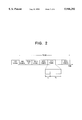
FIG. 2 illustrates the format of a DAB frame;
FIG. 3 illustrates the carrier-shifting operation of the first embodiment;
FIG. 4 is a block diagram of a second embodiment of the invention;
FIG. 5 is a block diagram of a third embodiment of the invention; and
FIG. 6 is a block diagram of a fourth embodiment of the invention.
DETAILED DESCRIPTION OF THE INVENTION
Embodiments of the invention will be described with reference to the attached illustrative drawings.
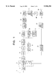
Referring to FIG. 1, the first embodiment is a digital receiver having an antenna 1, a radio-frequency amplifier (RF AMP) 2, a frequency converter 3 comprising a mixer (MIX) 31 and local oscillator (LO) 32, an intermediate-frequency amplifier (IF AMP) 5, an orthogonal demodulator (DEMOD) 6, an analog-to-digital converter (ADC) 7, a synchronization detector (SYNC DET) 8, a synchronization controller (SYNC CTL) 9, a discrete Fourier transform (DFT) processor 10, a differential demodulator (DIFF DEMOD) 11, a phase error detector 12, a frequency controller 13, a Viterbi decoder 14, an MPEG audio decoder 15, a digital-to-analog converter (DAC) 16, an audio amplifier 16, a loudspeaker 18, and a buffer memory 19. These elements are also found in conventional digital receivers. The local oscillator 32 is a voltage-controlled oscillator.
The novel elements in the first embodiment are a phase corrector 20, a carrier offset detector 21, and a carrier shifter 22. These elements are digital circuits that perform arithmetic and logic operations. Detailed circuit descriptions will be omitted to avoid obscuring the invention with unnecessary detail.
Incidentally, Viterbi decoding is a well-known type of maximum-likelihood decoding, and MPEG audio coding is a coding system recommended by the Motion Picture Experts Group (MPEG) and International Standards Organization (ISO).
The first embodiment is designed to receive a signal such as a DAB signal having the format shown in FIG. 2. The signal is divided into frames, each comprising two reference symbols followed by a fixed number of data symbols. The first reference symbol is a null symbol having zero amplitude, used for frame synchronization. The second reference symbol is a phase-reference symbol. Each data symbol comprises a guard interval of duration tG and a valid symbol interval of duration tS.
Frames of the type shown in FIG. 2 are transmitted simultaneously on K subcarrier signals, each modulated by differential quadrature phase-shift keying (DQPSK). K is an integer greater than one; in DAB mode one, for example, K is one thousand five hundred thirty-six (1536). The subcarrier signal frequencies are separated from one another by a subcarrier frequency spacing Δfc equal to the reciprocal of the valid symbol interval tS.
The subearriers are conventionally numbered in order of frequency from -K/2 to K/2. The central or zero-th subcarrier is not modulated.
The data transmitted in these frames are compressed audio data, encoded according to Layer Two of the MPEG-1 standard. The DAB recommendation establishes a specific order in which the coded audio data are assigned to the K subcarriers. For protection against transmission errors, the data are also convolutionally coded, and the convolutionally coded values are interleaved over a certain number of symbols.
Next, the operation of the first embodiment will be described.
Referring again to FIG. 1, the signal received at the antenna 1 is amplified by the radio-frequency amplifier 2 and down-converted in the mixer 31, by multiplication with the output of the local oscillator 32. Down-conversion produces an intermediate-frequency (IF) signal with frequency components equal to the difference between the frequency components present in the received signal and the frequency of the local oscillator 32.
The intermediate-frequency amplifier 5 amplifies the intermediate-frequency signal and rejects unwanted signal components such as adjacent-channel interference components. The resulting amplified intermediate-frequency signal is demodulated by an orthogonal demodulator 6, thereby being further down-shifted to a baseband frequency. The baseband signal is a complex-valued signal with an in-phase (I) component and a quadrature (Q) component.
The baseband signal is sampled and digitized by the analog-to-digital converter 7, then provided to the DFT processor 10, which performs a complex discrete Fourier transform on each symbol.
The baseband signal is also provided in analog form to the synchronization detector 8, which detects the envelope of the baseband signal. The synchronization detector 8 thereby detects the null symbol at the beginning of each frame. Based on the timing of the null symbol as reported by the synchronization detector 8, the synchronization controller 9 supplies the DFT processor 10 with timing signals that synchronize the DFT process with the symbols in each frame, establishing a window for the discrete Fourier transform performed on each symbol.
The discrete Fourier transform performed in the DFT processor 10 produces an array of, for example, two thousand forty-eight (2048) complex values representing the magnitude and phase of the baseband signal at an evenly-spaced set of frequencies, separated from one another by the subcarrier frequency spacing Δfc. The number of complex values in the array does not have to be two thousand forty-eight, but must exceed the number K of subcarriers by an amount sufficient to allow for anticipated differences in local-oscillator frequency between the transmitter (not shown) and receiver.
The array is stored in the buffer memory 19 for one symbol interval, then supplied to the differential demodulator 11. The array is also supplied to the phase corrector 20 and carrier offset detector 21. The carrier offset detector 21 detects a carrier offset, and the phase corrector 20 applies a corresponding phase correction, details of which will be described later.
The differential demodulator 11 takes the differences between the corrected phase values of the current array, which are obtained from the phase corrector 20, and the uncorrected phase values of the preceding array, which are read from the buffer memory 19. Due to the DQPSK modulation scheme employed in the DAB signal, if the frequency of the IF signal furnished to the orthogonal demodulator 6 is correct, at the subcarrier frequencies of the DAB signal, each phase difference will have one of the four values π/4, 3π/4, 5π/4, and 7π/4.
The phase error detector 12 multiplies the phase differences by four, divides the results by 2π, and takes the remainder. At DAB subcarrier frequencies, the remainder should always be equal to π; any deviation from π represents a phase error. The phase error detector 12 averages the difference between a certain number of these remainders and π to obtain a differential phase error ε If the frequency error ζ of the baseband signal is sufficiently small, it is related to the differential phase error ε by the following equation, in which Tsym is the duration of one symbol, including the guard interval.
ζ=ε/Tsym
The frequency controller 13 tunes the local oscillator 32 in a direction that reduces the differential phase error ε, thereby bringing ε to zero and holding ε substantially equal to zero. The size of the tuning adjustment can be calculated from the equation above. This tuning operation does not necessarily reduce the baseband frequency error ζ to zero, but brings ζ to an integer multiple of the subcarrier frequency spacing, so that for some integer m,
ζ-mΔf.sub.c.
The integer m is the carrier offset detected by the carrier offset detector 21.
Once the differential phase error ε has been corrected by the frequency controller 13, the array of values output by the differential demodulator 11 will contain correct data for the K subcarriers of the DAB signal. If the local oscillator 32 is correctly tuned in relation to the central subcarrier, the K subcarrier data values will occupy the central part of the array. If the local oscillator 32 is tuned to a different frequency, the positions of the subcarrier data will be shifted up or down in the array. This shift is also the carrier offset m detected by the carrier offset detector 21.
At the direction of the carrier offset detector 21, the carrier shifter 22 selects the K subcarrier data values from the array output by the differential demodulator 11. In effect, the carrier shifter 22 shifts the array by m positions to compensate for the carrier offset, then takes the K subcarrier data values from their normal positions in the shifted array.
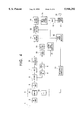
The carrier shifting operation is illustrated in FIG. 3. The solid arrows in FIG. 3 represent complex data in the differentially demodulated array. The numbers . . . , n, n+1, . . . , n+7, . . . correspond to array subscripts, and m is the carrier offset detected by the carrier offset detector 21. By shifting the data by m positions as indicated by the dotted arrows, the carrier shifter 22 compensates for the carrier offset. FIG. 3 illustrates a case in which the carrier offset is equivalent to twice the subcarrier frequency spacing, so the carrier shift is by two positions in the array.
As a result of this carrier shift, the carrier shifter 22 is able to furnish the Viterbi decoder 14 with K correctly arranged data values. The Viterbi decoder 14 de-interleaves and convolutionally decodes the data, thereby correcting data errors that may have occurred in transmission. The MPEG audio decoder 15 decodes the output of the Viterbi decoder 14 according to MPEG-1 decoding rules (Layer Two), thereby expanding the output of the Viterbi decoder 14 into a digital audio signal. The digital-to-analog converter 16 converts this signal to an analog signal, which is amplified by the audio amplifier 17 and reproduced through the loudspeaker 18.
Next, the operation of the phase corrector 20 and subcarrier offset detector 21 will be described in more detail.
The carrier offset detector 21 detects the carrier offset from the phase reference symbol. In the phase reference symbol, the k-th subcarrier is modulated to represent a fixed complex value zk equal to one of four values exp(jnπ/2) (where j is the square root of minus one and n=0, 1, 2, or 3). The signal waveform s(t) of the phase reference symbol can be represented by the following equation, in which ω is a fixed angular frequency, and t is a time variable. ##EQU1##
An array of complex conjugate values zk * of the phase reference values zk (k=-K/2 to K/2) is stored in the subcarrier offset detector 21, and is correlated with the array output by the DFT processor 10 under various assumed carrier offsets m. If the array output by the DFT processor 10 has values Z1k, the carrier offset detector 21 calculates products of the form Z1k-m zk *, the correlation being the sum of these products as k ranges from -K/2 to K/2. The integer m that yields the greatest correlation is detected as the carrier offset, and indicates the multiple of the subcarrier frequency spacing that is nearest to the actual frequency error ζ of the baseband signal.
The phase corrector 20 rotates the values output by the DFT processor 10 through a phase angle Q3 given by the following equation, in which m is the detected carrier offset, and tG and tS are the widths of the guard interval and valid symbol interval as shown in FIG. 2.
Q.sub.3 =-2×π×m×t.sub.G /t.sub.S
More specifically, the phase corrector 20 performs the following operation, where Rei,k and Imi,k are the real and imaginary parts of the output of the DFT processor 10 for the k-th subcarrier in the i-th symbol, and Re'i,k and Im'i,k are the real and imaginary parts as corrected by the phase corrector 20.
Re'.sub.i,k =Re.sub.i,k cos(Q.sub.3)-Im.sub.i,k sin(Q.sub.3)
Im'.sub.i,k =Re.sub.i,k sin(Q.sub.3)+Im.sub.i,k cos(Q.sub.3)
The reason for this phase correction is as follows.
Ideally, the local oscillator 32 is tuned in perfect relation to the central subcarrier frequency (k=0), there is no frequency error and no synchronization error, and no phase correction is necessary. The operation performed by the differential demodulator 11 can then be represented mathematically by the following equation, in which Z0i,k is the output of the DFT processor 10 for the k-th subcarrier in the i-th symbol, Qi,k is the phase angle in radians of Z0i,k, and Y0i,k is the output of the differential demodulator 11 for the k-th subcarrier in the i-th symbol. ##EQU2##
In practice, synchronization error in the timing of the DFT window leads to a certain phase error Q1, frequency error leads to a further phase error Of Q2 per symbol, and the above phase correction Q3 is applied. The differential demodulation operation is accordingly altered as in the following equation, in which Y1i,k and Z1i,k are the actual (non-ideal) outputs of the differential demodulator 11 and DFT processor 10, but Qi,k still represents the correct (ideal) phase angle. ##EQU3##
The actual differentially demodulated data will have the correct values when Y1i,k is equal to Y0i,k ; that is, when exp j(Q2 +Q3)! is equal to unity. This occurs when Q2 +Q3 is an integer multiple of 2π.
Q2 can be calculated as follows in terms of the baseband frequency error ζ and symbol interval Tsym.
Q.sub.2 =2×π×ζ×Tsym
Since the subcarrier frequency spacing Δfc is equal to the reciprocal of the valid symbol interval tS, the symbol interval Tsym has the following value.
Tsym=1/Δf.sub.c +t.sub.G
When the frequency error ζ is m times the subcarrier frequency spacing Δfc (m being an integer), Q2 has the following value. ##EQU4##
The following relations are therefore satisfied.
Q.sub.2 +Q.sub.3 =(2×π×m)
exp j(Q.sub.2 +Q.sub.3)!=1
Y1.sub.i,k =Y0.sub.i,k
The last of these relations means that, due to the phase correction Q3, the differentially demodulated data have the correct (ideal) values, despite the presence of the carrier offset. The phase correction Q3 cancels out the excess phase rotation that occurs during the guard interval, which cannot be corrected by the carrier shift.
The frequency control operation performed by the frequency controller 13 will now be reconsidered in terms of the carrier offset. Any baseband frequency error ζ can be expressed as an integer multiple of the subcarrier frequency spacing (mΔfc) and a portion ζ' which is less than the subcarrier frequency spacing. The phase error detector 12 detects only ζ'.
ζ'=ζ-mΔf.sub.c
Since an alteration in the frequency of the local oscillator produces an equal alteration in the baseband frequency, the frequency controller 13 needs to tune the local oscillator 32 only within a frequency range equivalent to one subcarrier frequency spacing Δfc to reduce ζ' to zero. A local oscillator 32 with a tuning range on the order of Δfc need not be expensive, and its tuning can easily be controlled with a high degree of accuracy.
The first embodiment accordingly obtains correctly demodulated data in a receiver using an inexpensive and accurately tunable local oscillator, despite the presence of a guard interval in the signal being received, without requiring the local oscillator to be tuned to the central subcarrier frequency.
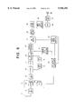
FIG. 4 illustrates a second embodiment of the invention, using the same reference numerals as in FIG. 1. The second embodiment differs from the first embodiment only in the position and operation of the phase corrector 20, which in the second embodiment adjusts the output of the buffer memory 19.
The phase correction Q4 applied by the phase corrector 20 in the second embodiment is equal in magnitude but opposite in sign to the phase correction Q3 applied in the first embodiment.
Q.sub.4 =-Q.sub.3 =2×π×m×t.sub.G /t.sub.S
The differential demodulation operation in the second embodiment can be described mathematically as follows, where Y2i,k is the actual output of the differential demodulator 11 and Y0i,k is, as before, the ideal value. ##EQU5##
The differentially demodulated output Y2i,k in the second embodiment is identical to the differentially demodulated output Y1i,k in the first embodiment. The second embodiment provides the same effects as the first embodiment.
FIG. 5 illustrates a third embodiment of the invention, again using the same reference numerals as in FIG. 1. The third embodiment also differs from the first embodiment only in the position and operation of the phase corrector 20, which is now disposed between the differential demodulator 11 and Viterbi decoder 14, and adjusts the phase values in the differentially demodulated array output by the differential demodulator 11.
The phase correction Q5 applied by the phase corrector 20 in the third embodiment is identical to the phase correction Q3 applied in the first embodiment.
Q.sub.5 =Q.sub.3 =-2×π×m×t.sub.G /t.sub.S
The differential demodulation operation and subsequent phase correction in the third embodiment can be described mathematically as follows, where Y3i,k is the output of the phase corrector 20. ##EQU6##
The values Y3i,k supplied to the Viterbi decoder 14 in the third embodiment are identical to the values Y1i,k supplied in the first embodiment. The third embodiment also provides the same effects as the first embodiment.
FIG. 6 illustrates a fourth embodiment of the invention, in which the operation of the frequency controller 13 is altered and the phase corrector is eliminated entirely. The carrier shifter 22 is now controlled by the frequency controller 13, instead of by the carrier offset detector 21. The other elements in the fourth embodiment are the same as in the preceding embodiments.
The phase corrections Q3, Q4, and Q5 in the preceding embodiments were equal to ±2×π×m×tG /tS. If m×tG /tS is an integer, the phase correction becomes an integer multiple of 2π, obviating the need for any actual correction. In the fourth embodiment, the frequency controller 13 operates so as to make m×tG /tS an integer.
The fourth embodiment makes use of the fact that the DAB guard interval tG is substantially equal to one-fourth the reciprocal of the subcarrier frequency spacing Δfc, or one-fourth the valid symbol interval tS. ##EQU7##
It follows that tG /tS is substantially equal to one-fourth, so if the carrier offset m is a multiple of four, m×tG /tS will be substantially an integer.
To deal with the general case, given that the valid symbol interval tS is the reciprocal of the subcarrier frequency spacing Δfc, let α be the closest integer to tS /tG. The phase correction becomes substantially unnecessary when the carrier shift is a multiple of α. For a DAB receiver, α is equal to four.
The local oscillator 32 in the fourth embodiment has a variable frequency range of at least α times the subcarrier frequency spacing. This enables the frequency controller 13 to adjust the local oscillator 32 to a frequency that makes the carrier offset m a multiple of α, as well as eliminating the phase error ε detected by the phase error detector 12.
Let Vc be the control voltage applied by the frequency controller 13 to the local oscillator 32, and let Vmin and Vmax by the minimum and maximum control voltages that can be applied. Let Dv be the amount by which the control voltage must be changed to alter the frequency of the local oscillator 32 by one subcarrier frequency spacing. The requirements for the tuning range of the local oscillator 32 can be given in terms of these quantities as follows.
Vmin≦Vc≦Vmax
Vmax-Vmin≧αDv
The carrier offset m detected by the carrier offset detector 21 at the present setting (Vc) can be expressed as the sum of an integer m" that is a multiple of α, plus another integer m' having an absolute value less than α. The frequency controller 13 calculates m" and m' by, for example, dividing the detected carrier offset by α, setting m" equal to the integer part of the quotient, and setting m' equal to the remainder. The carrier offset m will become a multiple of α, and m' will become zero, if the control voltage Vc is changed to the following voltage Vc'.
Vc'=Vc+m'Dv
If Vmin≦Vc'≦Vmax, the frequency controller 13 changes the control voltage of the local oscillator 32 to the above value Vc', and instructs the carrier shifter 22c to perform a carrier shift of m" on subsequent symbols.
If Vc'>Vmax, the frequency controller 13 changes the control voltage of the local oscillator 32 to the following value Vc', and instructs the carrier shifter 22 to perform a subcarrier shift of (m"+α) on subsequent symbols.
Vc'=Vc+(m'-α)Dv
If Vc'<Vmin, the frequency controller 13 changes the control voltage of the local oscillator 32 to the value Vc' given below, and instructs the carrier shifter 22 to perform a subcarrier shift of (m"-α) on subsequent symbols.
Vc'=Vc+(m'+α)Dv
In addition, the frequency controller 13 adjusts the control voltage Vc' to make the phase error ε detected by the phase error detector 12 equal to zero. This additional tuning adjustment is normally smaller then Dv, but if this adjustment would take the control voltage below Vmin or above Vmax, the frequency controller 13 adds or subtracts αDv to keep Vc' between Vmin and Vmax, and alters m" by subtracting or adding α.
In an alternate formulation of the above control rule, the carrier shifts to be performed by the carrier shifter 22 are given in terms of m' and the detected carrier offset m as follows: ##EQU8##
As a variation of the fourth embodiment, the carrier shifter 22 can be adapted to perform a carrier shift according to the carrier offset m detected by the carrier offset detector 21. Once the control voltage applied to the local oscillator 32 has been adjusted to Vc', the detected carrier offset m will become a multiple of α, m' will be zero, and correctly demodulated data will be obtained.
When the local oscillator 32 is tunable over a range equal to or greater than αΔfc, the fourth embodiment is preferable to the preceding embodiments in that the phase correction process can be eliminated. The fourth embodiment is advantageous when the quantity αΔfc is small enough that a local oscillator with a tuning range of αΔfc can still be inexpensive, and can still be tuned accurately.
Although described above in relation to the DAB recommendation, the present invention is applicable to any orthogonal frequency-division multiplexing that employs differential phase-shift keying, with valid symbol intervals separated by guard intervals.
The subcarrier frequency spacing does not have to be equal to the reciprocal of the valid symbol interval. The subcarrier frequency spacing may be any positive integer multiple of the reciprocal of the valid symbol interval.
The carrier offset detector was described as detecting the carrier offset by correlation of the phase reference symbol, but other methods of detecting the carrier offset can be employed, such as detecting the position of the unmodulated central subcarrier.
Those skilled in the art will recognize that further variations are possible within the scope claimed below.