US6009256A - Simulation/emulation system and method - Google Patents
Simulation/emulation system and method Download PDFInfo
- Publication number
- US6009256A US6009256A US08/850,136 US85013697A US6009256A US 6009256 A US6009256 A US 6009256A US 85013697 A US85013697 A US 85013697A US 6009256 A US6009256 A US 6009256A
- Authority
- US
- United States
- Prior art keywords
- hardware
- software
- model
- logic
- data
- Prior art date
- Legal status (The legal status is an assumption and is not a legal conclusion. Google has not performed a legal analysis and makes no representation as to the accuracy of the status listed.)
- Expired - Lifetime
Links
Images


Classifications
-
- G—PHYSICS
- G06—COMPUTING; CALCULATING OR COUNTING
- G06F—ELECTRIC DIGITAL DATA PROCESSING
- G06F30/00—Computer-aided design [CAD]
- G06F30/30—Circuit design
- G06F30/32—Circuit design at the digital level
- G06F30/33—Design verification, e.g. functional simulation or model checking
- G06F30/3308—Design verification, e.g. functional simulation or model checking using simulation
- G06F30/331—Design verification, e.g. functional simulation or model checking using simulation with hardware acceleration, e.g. by using field programmable gate array [FPGA] or emulation
-
- G—PHYSICS
- G06—COMPUTING; CALCULATING OR COUNTING
- G06F—ELECTRIC DIGITAL DATA PROCESSING
- G06F30/00—Computer-aided design [CAD]
- G06F30/30—Circuit design
- G06F30/32—Circuit design at the digital level
- G06F30/33—Design verification, e.g. functional simulation or model checking
Definitions
- the present invention generally relates to electronic design automation (EDA). More particularly, the present invention relates to a simulation and emulation system implemented in both software and hardware to verify electronic systems.
- EDA electronic design automation
- EDA electronic design automation
- EDA is a computer-based tool configured in various workstations to provide designers with automated or semi-automated tools for designing and verifying user's custom circuit designs.
- EDA is generally used for creating, analyzing, and editing any electronic design for the purpose of simulation, emulation, prototyping, execution, or computing.
- EDA technology can also be used to develop systems (i.e., target systems) which will use the user-designed subsystem or component.
- the end result of EDA is a modified and enhanced design, typically in the form of discrete integrated circuits or printed circuit boards, that is an improvement over the original design while maintaining the spirit of the original design.
- Co-simulation arose out of a need to address some problem with the cumbersome nature of using two separate and independent processes of pure software simulation and pure hardware emulation/acceleration, and to make the overall system more user-friendly.
- co-simulators still have a number of drawbacks: (1) co-simulation systems require manual partitioning, (2) co-simulation uses two loosely coupled engines, (3) co-simulation speed is as slow as software simulation speed, and (4) co-simulation systems encounter race conditions.
- partitioning between software and hardware is done manually, instead of automatically, further burdening the user.
- co-simulation requires the user to partition the design (starting with behavior level, then RTL, and then gate level) and to test the models themselves among the software and hardware at very large functional blocks. Such a constraint requires some degree of sophistication by the user.
- co-simulation systems utilize two loosely-coupled and independent engines, which raise inter-engine synchronization, coordination, and flexibility issues.
- Co-simulation requires synchronization of two different verification engines--software simulation and hardware emulation.
- the software simulator side is coupled to the hardware accelerator side, only external pin-out data is available for inspection and loading. Values inside the modeled circuit at the register and combinational logic level are not available for easy inspection and downloading from one side to the other, limiting the utility of these co-simulator systems.
- the user may have to re-simulate the whole design if the user switches from software simulation to hardware acceleration and back.
- co-simulator systems do not provide this capability.
- co-simulation speed is as slow as simulation speed.
- Co-simulation requires synchronization of two different verification engines--software simulation and hardware emulation.
- Each of the engines has its own control mechanism for driving the simulation or emulation. This implies that the synchronization between the software and hardware pushes the overall performance to a speed which is as low as software simulation.
- the additional overhead to coordinate the operation of these two engines adds to the slow speed of co-simulation systems.
- Co-simulators use hardware driven clocks, which may find themselves at the inputs to different logic elements at different times due to different wire line lengths. This raises the uncertainty level of evaluation results as some logic elements evaluate data at some time period and other logic elements evaluate data at different time periods, when these logic elements should be evaluating the data together.
- the present invention provides solutions to the aforementioned problems in the form of a flexible and fast simulation/emulation system, called herein as the "SEmulation system” or “SEmulator system.”
- One object of the present invention is to provide a system that provides the speed of a hardware accelerator with the control of a software simulator.
- Another object of the present invention is to provide a software simulator and a hardware accelerator with a single engine.
- Still another object of the present invention is to provide a system with different modes of operation (e.g., software simulation, hardware acceleration, ICE, and post-simulation analysis) and the ability to switch among these different modes with relative ease.
- modes of operation e.g., software simulation, hardware acceleration, ICE, and post-simulation analysis
- a further object of the present invention is to provide a system that automatically provides hardware and software models of the user's custom circuit design.
- Still yet another object of the present invention is to provide a means and method of avoiding race conditions in the hardware logic element or hardware accelerator.
- the SEmulation system and method of the present invention provide users the ability to turn their designs of electronic systems into software and hardware representations for simulation.
- the SEmulation system is a software-controlled emulator or a hardware-accelerated simulator and the methods used therein.
- pure software simulation is possible, but the simulation can also be accelerated through the use of the hardware model.
- Hardware acceleration is possible with software control for starting, stopping, asserting values, and inspecting values.
- In-circuit emulation mode is also available to test the user's circuit design in the environment of the circuit's target system. Again, software control is available.
- a software kernel that controls both the software and hardware models to provide greater run-time flexibility for the user by allowing the user to start, stop, assert values, inspect values, and switch among the various modes.
- the kernel controls the various modes by controlling data evaluation in the hardware via the enable inputs to the registers.
- the SEmulation system and method provide four modes of operation: (1) Software Simulation, (2) Simulation via Hardware Acceleration, (3) In-Circuit Emulation (ICE), and (4) Post-Simulation Analysis.
- the present invention is embodied in each of the above four modes or various combinations of these modes as follows: (1) Software Simulation alone; (2) Simulation via Hardware Acceleration alone; (3) In-Circuit Emulation (ICE) alone; (4) Post-Simulation Analysis alone; (5) Software Simulation and Simulation via Hardware Acceleration; (6) Software Simulation and ICE; (7) Simulation via Hardware Acceleration and ICE; (8) Software Simulation, Simulation via Hardware Acceleration, and ICE; (9) Software Simulation and Post-Simulation Analysis; (10) Simulation via Hardware Acceleration and Post-Simulation Analysis; (11) Software Simulation, Simulation via Hardware Acceleration, and Post-Simulation Analysis; (12) ICE and Post-Simulation Analysis; (13) Software Simulation, ICE, Post-Simulation Analysis; (14) Simulation via Hardware Acceleration,
- Each mode or combination of modes provides the following features or combinations of features: (1) Switching among modes, manually or automatically; (2) Usage--the user can switch among modes, and can start, stop, assert values, inspect values, and single-step cycle through the simulation or emulation process; (3) Compilation process to generate software models and hardware models; (4) Software kernel to control all modes with a main control loop that includes, in one embodiment, the steps of initialize system, evaluate active test-bench processes/components, evaluate clock components, detect clock edge, update registers and memories, propagate combinational components, advance simulation time, and continue the loop as long as active test-bench processes are present; (5) Component type analysis for generating hardware models; (6) mapping hardware models to reconfigurable4boards through, in one embodiment, clustering, placement, and routing; (7) software clock set-up to avoid race conditions through, in one embodiment, gated clock logic analysis and gated data logic analysis; (8) software clock implementation through, in one embodiment, clock edge detection in the software model to trigger an enable signal in the hardware model, send signal
- the simulation system operates in a host computer system for simulating a behavior of a circuit.
- the host computer system includes a central processing unit (CPU), main memory, and a local bus coupling the CPU to main memory and allowing communication between the CPU and main memory.
- the circuit has a structure and a function specified in a hardware language, such as HDL, which is capable of describing the circuit as component types and connections.
- the simulation system includes: a software model, a software control logic, and a hardware logic element.
- the software model of the circuit is coupled to the local bus. Typically, it resides in main memory.
- the software control logic is coupled to the software model and the hardware logic element, for controlling the operation of the software model and the hardware logic element.
- the software control logic includes interface logic which is capable of receiving input data and a clock signal from an external process, and a clock detection logic for detecting an active edge of the clock signal and generating a trigger signal.
- the hardware logic element is also coupled to the local bus and include a hardware model of at least a portion of the circuit based on component type, and a clock enable logic for evaluating data in the hardware model in response to the trigger signal.
- the hardware logic element also comprises an array or plurality of field programmable devices coupled together.
- Each field programmable device includes a portion of the hardware model of the circuit and thus, the combination of all the field programmable devices includes the entire hardware model.
- a plurality of interconnections also couple the portions of the hardware model together. Each interconnection represents a direct connection between any two field programmable devices located in the same row or column. The shortest path between any two field programmable devices in the array is at most two interconnections or "hops.”
- Another embodiment of the present invention is a system and method of simulating a circuit, where the circuit is modeled in software and at least a portion of the circuit is modeled in hardware.
- Data evaluation occurs in the hardware but is controlled in software via a software clock. Data to be evaluated propagates and stabilizes to the hardware model.
- the software model detects an active clock edge, it sends an enable signal to the hardware model to activate data evaluation.
- the hardware model evaluates the data and then waits for the new incoming data which may be evaluated at the next active clock edge signal detection in the software model.
- Another embodiment of the present invention includes a software kernel that controls the operation of the software model and the hardware model.
- the software kernel comprises the steps of evaluate active test-bench processes/components, evaluate clock components, detect clock edge, update registers and memories, propagate combinational components, advance simulation time, and continue the loop as long as active test-bench processes are present.
- a further embodiment of the present invention is a method of simulating a circuit, where the circuit has a structure and a function specified in a hardware language, such as HDL.
- the hardware language is also capable of describing or reducing the circuit into components.
- the method steps comprise: (1) determining component type in the hardware language; (2) generating a model of the circuit based on component type; and (3) simulating the behavior of the circuit with the model by providing input data to the model.
- Generating the model may include: (1) generating a software model of the circuit; and (2) generating a hardware model of the circuit based on component type.
- the present invention is a method of simulating a circuit.
- the steps include: (1) generating a software model of the circuit; (2) generating a hardware model of the circuit; (3) simulating a behavior of the circuit with the software model by providing input data to the software model; (4) selectively switching to the hardware model; (5) providing input data to the hardware model; and (6) simulating a behavior of the circuit with the hardware model by accelerating the simulation in the hardware model.
- the method may also include the additional steps of: (1) selectively switching to the software model; and (2) simulating a behavior of the circuit with the software model by providing input data to the software model. The simulation can also be stopped with the software model.
- the method comprises: (1) generating a software model of the circuit; (2) generating a hardware model of at least a portion of the circuit; (3) providing input signals from the target system to the hardware model; (4) providing output signals from the hardware model to the target system; (5) simulating a behavior of the circuit with the hardware model, where the software model is capable of controlling the simulation/emulation, cycle by cycle.
- the method of simulating a circuit comprises: (1) generating a model of the circuit; (2) simulating a behavior of the circuit with the model by providing input data to the model; and (3) logging selective input data and selective output data as log points from the model.
- a software and hardware model can be generated.
- the method may further comprise the steps of: (1) selecting a desired time-dependent point in the simulation; (2) selecting a log point at or prior to the selected time-dependent point; (3) providing input data to the hardware model; and (4) simulating a behavior of the circuit with the hardware model from the selected log point.
- a further embodiment of the present invention is a method of generating models for a simulation system for simulating a circuit.
- the steps include: (1) generating a software model of the circuit; (2) generating a hardware model for at least a portion of the circuit based on component type, said component type including register components and combinational components; and (3) generating a clock generation circuit in the hardware model to trigger data evaluation in the hardware model in response to clock edge detection in the software model.
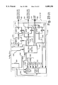
- FIG. 1 shows a high level overview of one embodiment of the present invention, including the workstation, reconfigurable hardware emulation model, emulation interface, and the target system coupled to a PCI bus.
- FIG. 2 shows one particular usage flow diagram of the present invention.
- FIG. 3 shows a high level diagram of the software compilation and hardware configuration during compile time and run time in accordance with one embodiment of the present invention.
- FIG. 4 shows a flow diagram of the compilation process, which includes generating the software/hardware models and the software kernel code.
- FIG. 5 shows the software kernel that controls the overall SEmulation system.
- FIG. 6 shows a method of mapping hardware models to reconfigurable boards through mapping, placement, and routing.
- FIG. 7 shows the connectivity matrix for the FPGA array shown in FIG. 8.
- FIG. 8 shows one embodiment of the 4 ⁇ 4 FPGA array and their interconnections.
- FIGS. 9(A), 9(B), and 9(C) illustrate one embodiment of the time division multiplexed (TDM) circuit which allows a group of wires to be coupled together in a time multiplexed fashion so that one pin, instead of a plurality of pins, can be used for this group of wires in a chip.
- FIG. 9(A) presents an overview of the pin-out problem
- FIG. 9(B) provides a TDM circuit for the transmission side
- FIG. 9(C) provides a TDM circuit for the receiver side.
- FIG. 10 shows a SEmulation system architecture in accordance with one embodiment of the present invention.
- FIG. 11 shows one embodiment of address pointer of the present invention.
- FIG. 12 shows a state transition diagram of the address pointer initialization for the address pointer of FIG. 11.
- FIG. 13 shows one embodiment of the MOVE signal generator for derivatively generating the various MOVE signals for the address pointer.
- FIG. 14 shows the chain of multiplexed address pointers in each FPGA chip.
- FIG. 15 shows one embodiment of the multiplexed cross chip address pointer chain in accordance with one embodiment of the present invention.
- FIG. 16 shows a flow diagram of the clock/data network analysis that is critical for the software clock implementation and the evaluation of logic components in the hardware model.
- FIG. 17 shows a basic building block of the hardware model in accordance with one embodiment of the present invention.
- FIGS. 18(A) and 18(B) show the register model implementation for latches and flip-flops.
- FIG. 19 shows one embodiment of the clock edge detection logic in accordance with one embodiment of the present invention.
- FIG. 20 shows a four state finite state machine to control the clock edge detection logic of FIG. 19 in accordance with one embodiment of the present invention.
- FIG. 21 shows the interconnection, JTAG, FPGA bus, and global signal pin designations for each FPGA chip in accordance with one embodiment of the present invention.
- FIG. 22 shows one embodiment of the FPGA controller between the PCI bus and the FPGA array.
- FIG. 23 shows a more detailed illustration of the CTRL -- FPGA unit and data buffer which were discussed with respect to FIG. 22.
- FIG. 24 shows the 4 ⁇ 4 FPGA array, its relationship to the FPGA banks, and expansion capability.
- FIG. 25 shows one embodiment of the hardware start-up method.
- FIG. 26 shows the HDL code for one example of a user circuit design to be modeled and simulated.
- FIG. 27 shows a circuit diagram that symbolically represent the circuit design of the HDL code in FIG. 26.
- FIG. 28 shows the component type analysis for the HDL code of FIG. 26.
- FIG. 29 shows a signal network analysis of a structured RTL HDL code based on the user's custom circuit design shown in FIG. 26.
- FIG. 30 shows the software/hardware partition result for the same hypothetical example.
- FIG. 31 shows a hardware model for the same hypothetical example.
- FIG. 32 shows one particular hardware model-to-chip partition result for the same hypothetical example of a user's custom circuit design.
- FIG. 33 shows another particular hardware model-to-chip partition result for the same hypothetical example of a user's custom circuit design.
- FIG. 34 shows the logic patching operation for the same hypothetical example of a user's custom circuit design.
- FIGS. 35(A) to 35(D) illustrate the principle of "hops" and interconnections with two examples.
- SEmulator or “SEmulation” system.
- SEmulation system software simulation
- SEmulator system simulation through hardware acceleration
- ICE in-circuit emulation
- post-simulation analysis including their respective set-up or pre-processing stages.
- SEmulation may be used. This term refers to the novel processes described herein.
- the specification also makes references to a "user” and a user's “circuit design” or “electronic design.”
- the "user” is a person who uses the SEmulation system through its interfaces and may be the designer of a circuit or a test/debugger who played little or no part in the design process.
- the "circuit design” or “electronic design” is a custom designed system or component, whether software or hardware, which can be modeled by the SEmulation system for test/debug purposes. In many cases, the "user” also designed the “circuit design” or “electronic design.”
- wire refers to various electrically conducting lines. Each line may be a single wire between two points or several wires between points. These terms are interchangeable in that a “wire” may comprise one or more conducting lines and a “bus” may also comprise one or more conducting lines.
- the various embodiments of the present invention have four general modes of operation: (1) software simulation, (2) simulation through hardware acceleration, (3) in-circuit emulation, and (4) post-simulation analysis.
- the various embodiments include the system and method of these modes with at least some of the following features:
- the end result is a flexible and fast simulator/emulator system and method with full HDL functionality and emulator execution performance.
- the SEmulator system through automatic component type analysis, can model the user's custom circuit design in software and hardware.
- the entire user circuit design is modeled in software, whereas evaluation components (i.e., register component, combinational component) are modeled in hardware.
- Hardware modeling is facilitated by the component type analysis.
- a software kernel residing in the main memory of the general purpose processor system, serves as the SEmulator system's main program that controls the overall operation and execution of its various modes and features. So long as any test-bench processes are active, the kernel evaluates active test-bench components, evaluates clock components, detects clock edges to update registers and memories as well as propagating combinational logic data, and advances the simulation time.
- This software kernel provides for the tightly coupled nature of the simulator engine with the hardware acceleration engine.
- the SEmulator system provides a number of I/O address spaces--REG (register), CLK (software clock), S2H (software to hardware), and H2S (hardware to software).
- the SEmulator has the capability to selectively switch among the four modes of operation.
- the user of the system can start simulation, stop simulation, assert input values, inspect values, single step cycle by cycle, and switch back and forth among the four different modes.
- the system can simulate the circuit in software for a time period, accelerate the simulation through the hardware model, and return back to software simulation mode.
- the SEmulation system provides the user with the capability to "see” every modeled component, regardless of whether it's modeled in software or hardware. For a variety of reasons, combinational components are not as “visible” as registers, and thus, obtaining combinational component data is difficult.
- FPGAs which are used in the reconfigurable board to model the hardware portion of the user's circuit design, typically model combinational components as look-up tables (LUT), instead of actual combinational components. Accordingly, the SEmulation system reads register values and then regenerates combinational components. Because some overhead is needed to regenerate the combinational components, this regeneration process is not performed all the time; rather, it is done only upon the user's request.
- a clock edge detection mechanism is provided to trigger the generation of a so-called software clock that drives the enable input to the various registers in the hardware model.
- the timing is strictly controlled through a double-buffered circuit implementation so that the software clock enable signal enters the register model before the data to these models.
- the software clock gates the data synchronously to ensure that all data values are gated together without any risk of hold-time violations.
- Software simulation is also fast because the system logs all input values and only selected register values/states, thus overhead is minimized by decreasing the number of I/O operations.
- the user can selectively select the logging frequency.
- the SEmulation system is capable of emulating the user's circuit within its target system environment.
- the target system outputs data to the hardware model for evaluation and the hardware model also outputs data to the target system.
- the software kernel controls the operation of this mode so that the user still has the option to start, stop, assert values, inspect values, single step, and switch from one mode to another.
- Logs provide the user with a historical record of the simulation session. Unlike known simulation systems, the SEmulation system does not log every single value, internal state, or value change during the simulation process. The SEmulation system logs only selected values and states based on a logging frequency (i.e., log 1 record every N cycles).
- a logging frequency i.e., log 1 record every N cycles.
- the SEmulation system implements an array of FPGA chips on a reconfigurable board. Based on the hardware model, the SEmulation system partitions, maps, places, and routes each selected portion of the user's circuit design onto the FPGA chips. Thus, for example, a 4 ⁇ 4 array of 16 chips may be modeling a large circuit spread out across these 16 chips.
- the interconnect scheme allows each chip to access another chip within 2 "jumps" or links.
- Each FPGA chip implements an address pointer for each of the I/O address spaces (i.e., REG, CLK, S2H, H2S).
- the combination of all address pointers associated with a particular address space are chained together. So, during data transfer, word data in each chip is sequentially selected from/to the main FPGA bus and PCI bus, one word at a time for the selected address space in each chip, and one chip at a time, until the desired word data have been accessed for that selected address space.
- This sequential selection of word data is accomplished by a propagating word selection signal. This word selection signal travels through the address pointer in a chip and then propagates to the address pointer in the next chip and continues on till the last chip or the system initializes the address pointer.
- the FPGA bus system in the reconfigurable board operates at twice the PCI bus bandwidth but at half the PCI bus speed.
- the FPGA chips are thus separated into banks to utilize the larger bandwidth bus.
- the throughput of this FPGA bus system can track the throughput of the PCI bus system so performance is not lost by reducing the bus speed. Expansion is possible through piggyback boards that extend the bank length.
- FIG. 1 shows a high level overview of one embodiment of the present invention.
- a workstation 10 is coupled to a reconfigurable hardware model 20 and emulation interface 30 via PCI bus system 50.
- the reconfigurable hardware model 20 is coupled to the emulation interface 30 via PCI bus 50, as well as cable 61.
- a target system 40 is coupled to the emulation interface 30 via cables 60.
- the in-circuit emulation set-up 70 which comprises the emulation interface 30 and target system 40 (as shown in the dotted line box) are not provided in this set-up when emulation of the user's circuit design within the target system's environment is not desired during a particular test/debug session. Without the in-circuit emulation set-up 70, the reconfigurable hardware model 20 communicates with the workstation 10 via the PCI bus 50.
- the reconfigurable hardware model 20 imitates or mimics the user's circuit design of some electronic subsystem in the target system.
- input and output signals between the target system 40 and the modeled electronic subsystem must be provided to the reconfigurable hardware model 20 for evaluation.
- the input and output signals of the target system 40 to/from the reconfigurable hardware model 20 are delivered via cables 60 through the emulation interface 30 and the PCI bus 50.
- input/output signals of the target system 40 can be delivered to the reconfigurable hardware model 20 via emulation interface 30 and cables 61.
- control data and some substantive simulation data pass between the reconfigurable hardware model 20 and the workstation 10 via the PCI bus 50.
- the workstation 10 runs the software kernel which controls the operation of the entire SEmulation system and must have access (read/write) to the reconfigurable hardware model 20.
- a workstation 10 complete with a computer, keyboard, mouse, monitor and appropriate bus/network interface allows a user to enter and modify data describing the circuit design of an electronic system.
- Exemplary workstations include a Sun Microsystems SPARC or ULTRA-SPARC workstation or an Intel/Microsoft-based computing station.
- the workstation 10 comprises a CPU 11, a local bus 12, a host/PCI bridge 13, memory bus 14, and main memory 15.
- the various software simulation, simulation by hardware acceleration, in-circuit emulation, and post-simulation analysis aspects of the present invention are provided in the workstation 10, reconfigurable hardware model 20, and emulation interface 30.
- the algorithm embodied in software is stored in main memory 15 during a test/debug session and executed through the CPU 11 via the workstation's operating system.
- control passes to its initialization code to set up necessary data structures, and load and initialize device drivers. Control is then passed to the command line interpreter (CLI), which prompts the user to indicate the program to be run.
- CLI command line interpreter
- the operating system determines the amount of memory needed to run the program, locates the block of memory, or allocates a block of memory and accesses the memory either directly or through BIOS. After completion of the memory loading process, the application program begins execution.
- One embodiment of the present invention is a particular application program for SEmulation.
- the application program may require numerous services from the operating system, including, but not limited to, reading from and writing to disk files, performing data communications, and interfacing with the display/keyboard/mouse.
- the workstation 10 has the appropriate user interface to allow the user to enter the circuit design data, edit the circuit design data, monitor the progress of simulations and emulations while obtaining results, and essentially control the simulation and emulation process.
- the user interface includes user-accessible menu-driven options and command sets which can be entered with the keyboard and mouse and viewed with a monitor.
- the user uses a computing station 80 with a keyboard 90.
- the user typically creates a particular circuit design of an electronic system and enters a HDL (usually structured RTL level) code description of his designed system into the workstation 10.
- the SEmulation system of the present invention performs component type analysis, among other operations, for partitioning the modeling between software and hardware.
- the SEmulation system models behavior, RTL, and gate level code in software.
- the system can model RTL and gate level code; however, the RTL level must be synthesized to gate level prior to hardware modeling.
- the gate level code can be processed directly into usable source design database format for hardware modeling. Using the RTL and gate level codes, the system automatically performs component type analysis to complete the partition step.
- the system maps some portion of the circuit design into hardware for fast simulation via hardware acceleration.
- the user can also couple the modeled circuit design to the target system for real environment in-circuit emulation. Because the software simulation and the hardware acceleration engines are tightly coupled, through the software kernel, the user can then simulate the overall circuit design using software simulation, accelerate the test/debug process by using the hardware model of the mapped circuit design, return to the simulation portion, and return to the hardware acceleration until the test/debug process is complete.
- the ability to switch between software simulation and hardware acceleration cycle-by-cycle and at will by the user is one of the valuable features of this embodiment.
- This feature is particularly useful in the debug process by allowing the user to go to a particular point or cycle very quickly using the hardware acceleration mode and then using software simulation to examine various points thereafter to debug the circuit design.
- the SEmulation system makes all components visible to the user whether the internal realization of the component is in hardware or software. The SEmulation system accomplishes this by reading the register values from the hardware model and then rebuilding the combinational components using the software model when the user requests such a read.
- the workstation 10 is coupled to a bus system 50.
- the bus system can be any available bus system that allows various agents, such as the workstation 10, reconfigurable hardware model 20, and emulation interface 30, to be operably coupled together.
- the bus system is fast enough to provide real-time or near real-time results to the user.
- One such bus system is the bus system described in the Peripheral Component Interconnect (PCI) standard, which is incorporated herein by reference.
- PCI Peripheral Component Interconnect
- revision 2.0 of the PCI standard provides for a 33 MHz bus speed.
- Revision 2.1 provides support for 66 MHz bus speed.
- the workstation 10, reconfigurable hardware model 20, and emulation interface 30 may comply with the PCI standard.
- PCI bus communication between the workstation 10 and the reconfigurable hardware model 20 is handled on the PCI bus.
- Other PCI-compliant devices may be found in this bus system. These devices may be coupled to the PCI bus at the same level as the workstation 10, reconfigurable hardware model 20, and emulation interface 30, or other levels.
- Each PCI bus at a different level, such as PCI bus 52 is coupled to another PCI bus level, such as PCI bus 50, if it exists at all, through a PCI-to-PCI bridge 51.
- PCI bus 52 two PCI devices 53 and 54 may be coupled therewith.
- the reconfigurable hardware model 20 comprises an array of field-programmable gate array (FPGA) chips that can be programmably configured and reconfigured to model the hardware portion of the user's electronic system design.
- the hardware model is reconfigurable; that is, it can reconfigure its hardware to suit the particular computation or user circuit design at hand. If, for example, many adders or multiplexers are required, the system is configured to include many adders and multiplexers. As other computing elements or functions are needed, they may also be modeled or formed in the system. In this way, the system can be optimized to perform specialized computations or logic operations. Reconfigurable systems are also flexible, so that users can work around minor hardware defects that arise during manufacture, testing, or use.
- the reconfigurable hardware model 20 comprises a two-dimensional array of computing elements consisting of FPGA chips to provide the computational resources for various user circuit designs and applications. More details on the hardware configuration process will be provided.
- the reconfigurable hardware model is reconfigurable via the use of field programmable devices.
- ASIC application specific integrated circuit
- Still other embodiments may be in the form of a custom integrated circuit.
- reconfigurable devices will be used to simulate/emulate the user's circuit design so that appropriate changes can be made prior to actual prototype manufacturing.
- an actual ASIC or custom integrated circuit can be used, although this deprives the user the ability to quickly and cost-effectively change a possibly non-functional circuit design for re-simulation and re-emulation.
- an ASIC or custom IC has already been manufactured and readily available so that emulation with an actual non-reconfigurable chip may be preferable.
- the software in the workstation along with its integration with an external hardware model, provides a greater degree of flexibility, control, and performance for the end user over existing systems.
- a model of the circuit design and the relevant parameters e.g., input test-bench stimulus, overall system output, intermediate results
- the user can use either schematic capture tools or synthesis tools to define the system circuit design.
- the user starts with a circuit design of an electronic system, usually in draft schematic form, which is then converted to HDL form using synthesis tools.
- the HDL can also be directly written by the user.
- Exemplary HDL languages include Verilog and VHDL; however, other languages are also available.
- a circuit design represented in HDL comprises many concurrent components. Each component is a sequence of code which either defines the behavior of a circuit element or controls the execution of the simulation.
- the SEmulation system analyzes these components to determine their component types and the compiler uses this component type information to build different execution models in software and hardware. Thereafter, the user can use the SEmulation system of the present invention. The designer can verify the accuracy of the circuit through simulation by applying various stimuli such as input signals and test vector patterns to the simulated model. If, during the simulation, the circuit does not behave as planned, the user re-defines the circuit by modifying the circuit schematic or the HDL file.
- the algorithm starts at step 100. After loading the HDL file into the system, the system compiles, partitions, and maps the circuit design to appropriate hardware models. The compilation, partition, and mapping steps are discussed in more detail below.
- One embodiment of the present invention uses a 2-bit wide data path to provide a 4-state value for the bus signal--"00" is logic low, "01” is logic high, “10” is “z” and "11” is “x.”
- software models can deal with “0,” “1,” "x” (bus conflicts or unknown value), and "z” (no driver or high impedance).
- hardware cannot deal with the unknown values "x,” so the reset sequence, which varies depending on the particular applicable code, resets the register values to all "0” or all "1.”
- step 105 the user decides whether to simulate the circuit design. Typically, a user will start the system with software simulation first. Thus, if the decision at step 105 resolves to "YES,” software simulation occurs at step 110.
- step 115 The user can stop the simulation to inspect values as shown in step 115. Indeed, the user can stop the simulation at any time during the test/debug session as shown by the dotted lines extending from step 115 to various nodes in the hardware acceleration mode, ICE mode, and post-simulation mode. Executing step 115 takes the user to step 160.
- step 115 branches to the stop/value inspect routine.
- the stop/value inspect routine starts at step 160.
- step 165 the user must decide whether to stop the simulation at this point and inspect values. If step 165 resolves to "YES,” step 170 stops the simulation that may be currently underway and inspects various values to check for correctness of the circuit design.
- step 175 the algorithm returns to the point at which it branched, which is at step 115.
- the user can continue to simulate and stop/inspect values for the remainder of the test/debug session or proceed forward to the in-circuit emulation step.
- step 120 the user decides whether to accelerate the test/debug process by accelerating the simulation through the hardware portion of the modeled circuit design. If the decision at step 120 resolves to "YES,” then hardware model acceleration occurs at step 125.
- the SEmulation system mapped some portions into a hardware model.
- the system moves register and combinational components into the hardware model and moves the input and evaluation values to the hardware model.
- the evaluation occurs in the hardware model for a long time period at the accelerated speed.
- the kernel writes test-bench output to the hardware model, updates the software clock, then reads the hardware model output values cycle-by-cycle.
- values from the entire software model of the user's circuit design which is the entire circuit design, can be made available by outputting register values and combinational components by regenerating combinational components with the register values. Because of the need for software intervention to regenerate these combinational components, outputs of values for the entire software model are not provided at every cycle; rather, values are provided to the user only if the user wants such values. This specification will discuss the combinational component regeneration process later.
- the user can stop the hardware acceleration mode at any time as indicated by step 115. If the user wants to stop, the algorithm proceeds to steps 115 and 160 to branch to the stop/value inspect routine.
- the user can stop the hardware accelerated simulation process at any time and inspect values resulting from the simulation process, or the user can continue with the hardware-accelerated simulation process.
- the stop/value inspect routine branches to steps 160, 165, 170, and 175, which were discussed above in the context of stopping the simulation.
- the user can decide to continue with the hardware-accelerated simulation or perform pure simulation instead at step 135. If the user wants to simulate further, the algorithm proceeds to step 105. If not, the algorithm proceeds to the post-simulation analysis at step 140.
- the SEmulation system provides a number of post-simulation analysis features.
- the system logs all inputs to the hardware model.
- the system logs all values of hardware register components at a user-defined logging frequency (e.g., 1/10,000 record/cycle).
- the logging frequency determines how often the output values are recorded.
- output values are recorded once every 10,000 cycles.
- the higher the logging frequency the more information is recorded for later post-simulation analysis.
- the user selects the logging frequency with care. A higher logging frequency will decrease the SEmulation speed because the system must spend time and resources to record the output data by performing I/O operations to memory before further simulation can be performed.
- the user selects a particular point at which simulation is desired.
- the user can then perform analysis after SEmulation by running the software simulation with input logs to the hardware model to compute the value changes and internal states of all hardware components.
- the hardware accelerator is used to simulate the data from the selected logging point to analyze simulation results.
- This post-simulation analysis method can link to any simulation waveform viewer for post-simulation analysis. More detailed discussion will follow.
- step 145 the user can opt to emulate the simulated circuit design within its target system environment. If step 145 resolves to "NO,” the algorithm ends and the SEmulation process ends at step 155. If emulation with the target system is desired, the algorithm proceeds to step 150. This step involves activating the emulation interface board, plugging the cable and chip pin adapter to the target system, and running the target system to obtain the system I/O from the target system.
- the system I/O from the target system includes signals between the target system and the emulation of the circuit design.
- the emulated circuit design receives input signals from the target system, processes these, sends them to the SEmulation system for further processing, and outputs the processed signals to the target system.
- the emulated circuit design sends output signals to the target system, which processes these, and possibly outputs the processed signals back to the emulated circuit design.
- the performance of the circuit design can be evaluated in its natural target system environment.
- the user After the emulation with the target system, the user has results that validate the circuit design or reveal non-functional aspects. At this point, the user can simulate/emulate again as indicated at step 135, stop altogether to modify the circuit design, or proceed to integrated circuit fabrication based on the validated circuit design.
- FIG. 3 shows two sets of information: one set of information distinguishes the operations performed during compile time and simulation/emulation run time; and the other set of information shows the partitioning between software models and hardware models.
- the SEmulation system in accordance with one embodiment of the present invention needs the user circuit design as input data 200.
- the user circuit design is in some form of HDL file (e.g., Verilog, VHDL).
- the SEmulation system parses the HDL file so that behavior level code, register transfer level code, and gate level code can be reduced to a form usable by the SEmulation system.
- the system generates a source design database for front end processing step 205.
- the processed HDL file is now usable by the SEmulation system.
- the parsing process converts ASCII data to an internal binary data structure and is known to those ordinarily skilled in the art. Please refer to ALFRED V. AHO, RAVI SETHI, AND JEFFREY D. ULLMAN, COMPILERS: PRINCIPLES, TECHNIQUES, AND TOOLS (1988), which is incorporated by reference herein.
- Compile time is represented by processes 225 and run time is represented by processes/elements 230.
- the SEmulation system compiles the processed HDL file by performing component type analysis.
- the component type analysis classifies HDL components into combinational components, register components, clock components, memory components, and test-bench components. Essentially, the system partitions the user circuit design into control and evaluation components.
- the SEmulation compiler 210 essentially maps the control components of the simulation into software and the evaluation components into software and hardware.
- the compiler 210 generates a software model for all HDL components.
- the software model is cast in code 215. Additionally, the SEmulation compiler 210 uses the component type information of the HDL file, selects or generates hardware logic blocks/elements from a library or module generator, and generates a hardware model for certain HDL components. The end result is a so-called "bitstream" configuration file 220.
- the software model in code form is stored in main memory where the application program associated with the SEmulation program in accordance with one embodiment of the present invention is stored.
- This code is processed in the general purpose processor or workstation 240.
- the configuration file 220 for the hardware model is used to map the user circuit design into the reconfigurable hardware boards 250.
- those portions of the circuit design that have been modeled in hardware are mapped and partitioned into the FPGA chips in the reconfigurable hardware boards 250.
- test-bench stimulus and test vector data as well as other test-bench resources 235 are applied to the general purpose processor or workstation 240 for simulation purposes.
- the user can perform emulation of the circuit design via software control.
- the reconfigurable hardware boards 250 contain the user's emulated circuit design. This SEmulation system has the ability to let the user selectively switch between software simulation and hardware emulation, as well as stop either the simulation or emulation process at any time, cycle-by-cycle, to inspect values from every component in the model, whether register or combinational.
- the SEmulation system passes data between the test-bench 235 and the processor/workstation 240 for simulation and the test-bench 235 and the reconfigurable hardware boards 250 via data bus 245 and processor/workstation 240 for emulation.
- emulation data can pass between the reconfigurable hardware boards 250 and the target system 260 via the emulation interface 255 and data bus 245.
- the kernel is found in the software simulation model in the memory of the processor/workstation 240 so data necessarily pass between the processor/workstation 240 and the reconfigurable hardware boards 250 via data bus 245.
- FIG. 4 shows a flow chart of the compilation process in accordance with one embodiment of the present invention.
- the compilation process is represented as processes 205 and 210 in FIG. 3.
- the compilation process in FIG. 4 starts at step 300.
- Step 301 processes the front end information.
- gate level HDL code is generated.
- the user has converted the initial circuit design into HDL form by directly handwriting the code or using some form of schematic or synthesis tool to generate the gate level HDL representations of the code.
- the SEmulation system parses the HDL file (in ASCII format) into a binary format so that behavior level code, register transfer level (RTL) code, and gate level code can be reduced to an internal data structure form usable by the SEmulation system.
- the system generates a source design database containing the parsed HDL code.
- Step 302 performs component type analysis by classifying HDL components into combinational components, register components, clock components, memory components, and test-bench components as shown in component type resource 303.
- the SEmulation system generates hardware models for register and combinational components, with some exceptions as discussed below.
- Test-bench and memory components are mapped in software.
- Some clock components e.g., derived clocks
- Combinational components are stateless logic components whose output values are a function of current input values and do not depend on the history of input values.
- Examples of combinational components include primitive gates (e.g., AND, OR, XOR, NOT), selector, adder, multiplier, shifter, and bus drivers.
- Register components are simple storage components. The state transition of a register is controlled by a clock signal.
- One form of register is edge-triggered which may change states when an edge is detected.
- Another form of register is a latch which is level triggered. Examples include flip-flops (D-type, JK-type) and level-sensitive latches.
- Clock components are components that deliver periodic signals to logic devices to control their behavior. Typically, clock signals control the update of registers.
- Primary clocks are generated from self-timed test-bench processes. For example, a typical test-bench process for clock generation in Verilog is as follows:
- the clock signal is initially at logic "0.” After 5 time units, the clock signal changes to logic "1.” After 5 time units, the clock signal reverts back to logic "0.”
- the primary clock signals are generated in software and only a few (i.e., 1-10) primary clocks are found in a typical user circuit design. Derived or gated clocks are generated from a network of combinational logic and registers which are in turn driven by the primary clocks. Many (i.e., 1,000 or more) derived clocks are found in a typical user circuit design.
- Memory components are block storage components with address and control lines to access individual data in specific memory locations. Examples include ROM, asynchronous RAM, and synchronous RAM.
- Test-bench components are software processes used to control and monitor the simulation processes. Accordingly, these components are not part of the hardware circuit design under test. Test-bench components control the simulation by generating clock signals, initializing simulation data, and reading simulation test vector patterns from disk/memory. Test-bench components also monitor the simulation by checking for changes in value, performing value change dump, checking asserted constraints on signal value relations, writing output test vectors to disk/memory, and interfacing with various waveform viewers and debuggers.
- the SEmulation system performs component type analysis as follows. The system examines the binary source design database. Based on the source design database, the system can characterize or classify the elements as one of the above component types. Continuous assignment statements are classified as combinational components. Gate primitives are either combinational type or latch form of register type by language definition. Initialization code are treated as test-benches of initialization type.
- An always process that drives nets without using the nets is a test-bench of driver type.
- An always process that read s nets without driving the nets is a test-bench of monitor type.
- An always process with delay controls or multiple event controls are test-benches of general type.
- An always process with a single event control and driving a single net can be one of the following: (1) If the event control is edge-triggered event, then the process is an edge-triggered type register component. (2) If a net driven in a process is not defined in all possible execution paths, then the net is a latch type of register. (3) If a net driven in a process is defined in all possible execution paths, then the net is a combinational component.
- An always process with a single event control but driving multiple nets can be decomposed into several processes driving each net separately to derive their respective component types separately.
- the decomposed processes can then be used to determine component type.
- Step 304 generates a software model for all HDL components regardless of component type.
- the user is capable of simulating the entire circuit design using the complete software model.
- Test-bench processes are used to drive the stimulus input, test vector patterns, control the overall simulation, and monitor the simulation process.
- Step 305 performs clock analysis.
- the clock analysis includes two general steps: (1) clock extraction and sequential mapping, and (2) clock network analysis.
- the clock extraction and sequential mapping step includes mapping the user's register components into the SEmulation system's hardware register model and then extracting clock signals out of the system's hardware register components.
- the clock network analysis step includes determining primary clocks and derived clocks based on the extracted clock signals, and separating the gated clock network and gated data network. A more detailed description will be provided with respect to FIG. 16.
- Step 306 performs residence selection.
- the system in conjunction with the user, selects the components for hardware models; that is, of the universe of possible hardware components that can be implemented in the hardware model of the user's circuit design, some hardware components will not be modeled in hardware for a variety of reasons. These reasons include component types, hardware resource constraints (i.e., floating point operations and large multiply operations stay in software), simulation and communication overhead (i.e., small bridge logic between test-bench processes stay in software, and signals that are monitored by test-bench processes stay in software), and user preferences. For a variety of reasons including performance and simulation monitoring, the user can force certain components that would otherwise be modeled in hardware to stay in software.
- Step 307 maps the selected hardware models into a reconfigurable hardware emulation board.
- step 307 maps takes the netlist and maps the circuit design into specific FPGA chips. This step involves grouping or clustering logic elements together. The system then assigns each group to a unique FPGA chip or several groups to a single FPGA chip. The system may also split groups to assign them to different FPGA chips. In general, the system assigns groups to FPGA chips. More detailed discussion will be provided below with respect to FIG. 6. The system places the hardware model components into a mesh of FPGA chips to minimize inter-chip communication overhead.
- the array comprises a 4 ⁇ 4 array of FPGAs, a PCI interface unit, and a software clock control unit.
- the array of FPGAs implements a portion of the user's hardware circuit design, as determined above in steps 302-306 of this software compilation process.
- the PCI interface unit allows the reconfigurable hardware emulation model to communicate with the workstation via the PCI bus.
- the software clock avoids race conditions for the various clock signals to the array of FPGAs.
- step 307 routes the FPGA chips according to the communication schedule among the hardware models.
- the stitching logic of step 308 inserts the control circuits.
- These control circuits include the I/O address pointers and data bus logic for communication with the DMA engine to the simulator (discussed below with respect to FIGS. 11, 12, and 14), and the evaluation control logic to control hardware state transitions and wire multiplexing (discussed below with respect to FIGS. 19 and 20).
- a direct memory access (DMA) unit provides an additional data channel between peripherals and main memory in which the peripherals can directly access (i.e., read, write) the main memory without the intervention of the CPU.
- the address pointer in each FPGA chip allows data to move between the software model and the hardware model in light of the bus size limitations.
- the evaluation control logic is essentially a finite state machine that ensures that the clock enable inputs to registers to be asserted before the clock and data inputs enter these registers.
- Step 309 generates the configuration files for mapping the hardware model to FPGA chips. In essence, step 309 assigns circuit design components to specific cells or gate level components in each chip. Whereas step 307 determines the mapping of hardware model groups to specific FPGA chips, step 309 takes this mapping result and generates a configuration file for each FPGA chip.
- Step 310 generates the software kernel code.
- the kernel is a sequence of software code that controls the overall SEmulation system. The kernel cannot be generated until this point because portions of the code require updating and evaluating hardware components. Only after step 309 has the appropriate mapping to hardware models and FPGA chips occurred. More detailed discussion will be provided below with respect to FIG. 5. The compilation ends at step 311.
- the software kernel code is generated in step 310 after the software and hardware models have been determined.
- the kernel is a piece of software in the SEmulation system that controls the operation of the overall system.
- the kernel controls the execution of the software simulation as well as the hardware emulation. Because the kernel also resides in the center of the hardware model, the simulator is integrated with the emulator.
- the SEmulation system in accordance with one embodiment of the present invention does not require the simulator to interact with the emulator from the outside.
- One embodiment of the kernel is a control loop shown in FIG. 5.
- the kernel begins at step 330.
- Step 331 evaluates the initialization code.
- the control loop begins and cycles repeatedly until the system observes no active test-bench processes, in which case the simulation or emulation session has completed.
- Step 332 evaluates the active test-bench components for the simulation or emulation.
- Step 333 evaluates clock components. These clock components are from the test-bench process. Usually, the user dictates what type of clock signal will be generated to the simulation system. In one example (discussed above with respect to component type analysis and reproduced here), a clock component as designed by a user in the test-bench process is as follows:
- the user has decided, in this clock component example, that a logic "0" signal will be generated first, and then after 5 simulation times later, a logic "1" signal will be generated. This clock generation process will cycle continuously until stopped by the user. These simulation times are advanced by the kernel.
- Step 334 inquires whether any active clock edge is detected, which would result in some kind of logic evaluation in the software and possible hardware model (if emulation is running).
- the clock signal which the kernel uses to detect an active clock edge is the clock signal from the test-bench process. If the decision step 334 evaluates to "NO,” then the kernel proceeds to step 337. If the decision step 334 evaluates to "YES,” resulting in step 335 updating registers and memories, and step 336 propagating combinational components. Step 336 essentially takes care of combinational logic which needs some time to propagate values through the combinational logic network after a clock signal has been asserted. Once the values have propagated through the combinational components and stabilized, the kernel proceeds to step 337.
- the kernel controls the emulator portion of the SEmulation system.
- the kernel can accelerate the evaluation of the hardware model in steps 334 and 335 whenever any active clock edge is detected.
- the SEmulation system in accordance with one embodiment of the present invention can accelerate the hardware emulator through the software kernel and based on component type (e.g., register, combinational).
- the kernel controls the execution of the software and hardware model cycle by cycle.
- the emulator hardware model can be characterized as a simulation coprocessor to the general-purpose processor running the simulation kernel. The coprocessor speeds up the simulation task.
- Step 337 evaluates active test-bench components.
- Step 338 advances the simulation time.
- Step 339 provides the boundary for the control loop that begins at step 332.
- Step 339 determines whether any test-bench processes are active. If so, the simulation and/or emulation is still running and more data should be evaluated.
- the kernel loops to step 332 to evaluate any active test-bench components. If no test-bench processes are active, then the simulation and emulation processes have completed.
- Step 340 ends the simulation/emulation process.
- the kernel is the main control loop that controls the operation of the overall SEmulation system. So long as any test-bench processes are active, the kernel evaluates active test-bench components, evaluates clocks components, detects clock edges to update registers and memories as well as propagate combinational logic data, and advances the simulation time.
- FIG. 6 shows one embodiment of a method of automatically mapping hardware models to reconfigurable boards.
- a netlist file provides the input to the hardware implementation process.
- the netlist describes logic functions and their interconnections.
- the hardware model-to-FPGA implementation process includes three independent tasks: mapping, placement, and routing.
- the tools are generally referred to as "place-and-route" tools.
- the design tool used may be Viewlogic Viewdraw, a schematic capture system, and Xilinx Xact place and route software, or Altera's MAX+PLUS II system.
- the mapping task partitions the circuit design into the logic blocks, I/O blocks, and other FPGA resources. Although some logic functions such as flip-flops and buffers may map directly into the corresponding FPGA resource, other logic functions such as combinational logic must be implemented in logic blocks using mapping algorithms. The user can usually select mapping for optimal density or optimal performance.
- the placement task involves taking the logic and I/O blocks from the mapping task and assigning them to physical locations within the FPGA array.
- Current FPGA tools generally use some combination of three techniques: mincut, simulating annealing, and general force-directed relaxation (GFDR). These techniques essentially determine optimal placement based on various cost functions which depend on total net length of interconnections or the delay along a set of critical signal paths, among other variables.
- the Xilinx XC4000 series FPGA tools use a variation of the mincut technique for initial placement followed by a GFDR technique for fine improvement in the placement.
- the routing task involves determining the routing paths used to interconnect the various mapped and placed blocks.
- One such router called a maze router, seeks the shortest path between two points. Since the routing task provides for direct interconnection among the chips, the placement of the circuits with respect to the chips is critical.
- the hardware model can be described in either gate netlist 350 or RTL 357.
- the RTL level code can be further synthesized to gate level netlist.
- a synthesizer server 360 such as the Altera MAX+PLUS II programmable logic development tool system and software, can be used to produce output files for mapping purposes.
- the synthesizer server 360 has the ability to match the user's circuit design components to any standard existing logic elements found in a library 361 (e.g., standard adders or standard multipliers), generate any parameterized and frequently used logic module 362 (e.g., non-standard multiplexers or non-standard adders), and synthesize random logic elements 363 (e.g., look-up table-based logic that implements a customized logic function).
- the synthesizer server also removes redundant logic and unused logic.
- the output files essentially synthesize or optimize the logic required by the user's circuit design.
- the synthesizer server is capable of generating any logic element based on variations of standard logic elements or random logic elements that may not have any parallels in these variations or library standard logic elements.
- the SEmulation system will initially perform the grouping or clustering operation 351.
- the hardware model construction is based on the clustering process because the combinational logic and registers are separated from the clock. Thus, logic elements that share a common primary clock or gated clock signal may be better served by grouping them together and placed on a chip together.
- the clustering algorithm is based on connectivity driven, hierarchical extraction, and regular structure extraction. If the description is in structured RTL 358, the SEmulation system can decompose the function into smaller units as represented by the logic function decomposition operation 359. At any stage, if logic synthesis or logic optimization is required, a synthesizer server 360 is available to transform the circuit design to a more efficient representation based on user directives.
- the link to the synthesizer server is represented by dotted arrow 364.
- the link to the synthesizer server 360 is represented by arrow 365.
- the link to the synthesizer server 360 is represented by arrow 366.
- the clustering operation 351 groups the logic components together in a selective manner based on function and size.
- the clustering may involve only one cluster for a small circuit design or several clusters for a large circuit design. Regardless, these clusters of logic elements will be used in later steps to map them into the designated FPGA chips; that is, one cluster will be targeted for a particular chip and another cluster will be targeted for a different chip or possibly the same chip as the first cluster.
- the logic elements in a cluster will stay together with the cluster in a chip, but for optimization purposes, a cluster may have to be split up into more than one chip.
- the system After the clusters are formed in the clustering operation 351, the system performs a place-and-route operation. Initially, a coarse-grain placement operation 352 of the clusters into the FPGA chips is performed. The coarse-grain placement operation 352 initially places clusters of logic elements to selected FPGA chips. If necessary, the system makes the synthesizer server 360 available to the coarse-grain placement operation 352 as represented by arrow 367. A fine-grain placement operation is performed after the coarse-grain placement operation to fine-tune the initial placement. The SEmulation system uses a cost function based on pin usage requirements, gate usage requirements, and gate-to-gate hops to determine the optimal placement for both the coarse-grain and fine-grain placement operations.
- the user's circuit design that is modeled in the hardware model comprises the total combination of circuits CKTQ.
- Each cost function is defined such that the computed values of the calculated placement cost tend to generally promote: (1) a minimum number of "hops" between any two circuits CKTN-1 and CKTN in the FPGA array, and (2) placement of circuits CKTN-1 and CKTN in the FPGA array such that pin usage is minimized.
- the cost function F(P, G, D) is defined as: ##EQU1##
- the first term (i.e., C0*P) generates a first placement cost value based on the number of pins used and the number pins available.
- the second term (i.e., C1*G) generates a second placement cost value based on the number of gates used and the number of gates available.
- the third term (i.e., C2*D) generates a placement cost value based on the number of hops present between various interconnecting gates in the circuits CKTQ (i.e., CKT1, CKT2, . . . , CKTN).
- the overall placement cost value is generated by iteratively summing these three placement cost values.
- Constants C0, C1, and C2 represent weighting constants that selectively skew the overall placement cost value generated from this cost function toward the factor or factors (i.e., pin usage, gate usage, or gate-to-gate hops) that is/are most important during any iterative placement cost calculation.
- the placement cost is calculated repeatedly as the system selects different relative values for the weighting constants C0, C1, and C2.
- the system selects large values for C0 and C1 relative to C2.
- the system determines that optimizing pin usage/availability and gate usage/availability are more important than optimizing gate-to-gate hops in the initial placement of the circuits CKTQ in the array of FPGA chips.
- the system selects small values for C0 and C1 relative to C2.
- the system determines that optimizing gate-to-gate hops is more important than optimizing pin usage/availability and gate usage/availability.
- the system uses the same cost function.
- the iterative steps with respect to the selection of C0, C1, and C2 are the same as for the coarse-grain operation.
- the fine-grain placement operation involves having the system select small values for C0 and C1 relative to C2.
- the cost function examines pin usage/availability (P), gate usage/availability (G), and gate-to-gate hops (D). Based on the cost function variables, P, G, and D, the cost function f(P, G, D) generates a placement cost value for placing circuits CKTQ in particular locations in the FPGA array.
- Pin usage/availability P also represents the I/O capacity.
- P used is the number of used pins by the circuits CKTQ for each FPGA chip.
- P available is the number of available pins in the FPGA chip. In one embodiment, is P available is 264 (44 pins ⁇ 6 interconnections/chip), while in another embodiment, P available is 265 (44 pins ⁇ 6 interconnections/chip+1 extra pin).
- P available is 264 (44 pins ⁇ 6 interconnections/chip), while in another embodiment, P available is 265 (44 pins ⁇ 6 interconnections/chip+1 extra pin).
- the specific number of available pins depends on the type of FPGA chip used, the total number of interconnections used per chip, and the number of pins used for each interconnection. Thus, P available can vary considerably.
- the ratio P used /P available is calculated for each FPGA chip.
- sixteen ratios P used /P available are calculated. The more pins are used for a given number of available pins, the higher the ratio. Of the sixteen calculated ratios, the ratio yielding the highest number is selected.
- the first placement cost value is calculated from the first term C0*P by multiplying the selected maximum ratio P used /P available with the weighting constant C0.
- this first term depends on the calculated ratio P used /P available and the particular maximum ratio among the ratios calculated for each FPGA chip, the placement cost value will be higher for higher pin usage, all other factors being equal.
- the system selects the placement yielding the lowest placement cost.
- the particular placement yielding a maximum ratio P used /P available that is the lowest among all the maximums calculated for various placements is generally considered as the optimum placement in the FPGA array, all other factors being equal.
- the gate usage/availability G is based on the number of gates allowable by each FPGA chip. In one embodiment, based on the location of the circuits CKTQ in the array, if the number of gates used G used in each chip is above a certain threshold, then this second placement cost (C1*G) will be assigned a value indicating that the placement is not feasible. Analogously, if the number of gates used in each chip containing circuits CKTQ is at or below a certain threshold, then this second term (C1*G) will be assigned a value indicating that the placement is feasible.
- the system may conclude through the cost function that this particular placement is infeasible.
- the high number e.g., infinity
- G ensures that the cost function will generate a high placement cost value indicating that the desired placement of the circuits CKTQ is not feasible and that an alternative placement should be determined.
- the ratio G used /G available is calculated for each chip, where G used is the number of gates used by the circuits CKTQ in each FPGA chip, and G available is the number of gates available in each chip.
- the system uses the FLEX 10K100 chip for the FPGA array.
- the FLEX 10K100 chip contains approximately 100,000 gates.
- G available is equal to 100,000 gates.
- sixteen ratios G used /G available are calculated. The more gates are used for a given number of available gates, the higher the ratio. Of the sixteen calculated ratios, the ratio yielding the highest number is selected.
- the second placement cost value is calculated from the second term C1*G by multiplying the selected maximum ratio G used /G available with the weighting constant C1. Because this second term depends on the calculated ratio G used /G available and the particular maximum ratio among the ratios calculated for each FPGA chip, the placement cost value will be higher for higher gate usage, all other factors being equal.
- the system selects the circuit placement yielding the lowest placement cost.
- the particular placement yielding a maximum ratio G used /G available that is the lowest among all the maximums calculated for various placements is generally considered as the optimum placement in the FPGA array, all other factors being equal.
- the system selects some value for C1 initially. If the ratio G used /G available is greater than "1," then this particular placement is infeasible (i.e., at least one chip does not have enough gates for this particular placement of circuits). As a result, the system modifies C1 with a very high number (e.g., infinity) and accordingly, the second term C1*G will also be a very high number and the overall placement cost value f(P, G, D) will also be very high. If, on the other hand, the ratio G used /G available is less than or equal to "1,” then this particular placement is feasible (i.e., each chip has enough gates to support the circuit implementation). As a result, the system does not modify C1 and accordingly, the second term C1*G will resolve to a particular number.
- the third term C2*D represents the number of hops between all gates that require interconnection.
- the number of hops also depends on the interconnection matrix.
- the connectivity matrix provides the foundation for determining circuit paths between any two gates that need chip-to-chip interconnection. Not every gate needs the gate-to-gate interconnection. Based on the user's original circuit design and the partitioning of clusters to certain chips, some gates will not need any interconnection whatsoever because the logic element(s) connected to their respective input(s) and output(s) is/are located in the same chip. Other gates, however, need the interconnections because the logic element(s) connected to their respective input(s) and output(s) is/are located in different chips.
- each interconnection between chips such as interconnection 602 between chip F11 and chip F14, represents 44 pins or 44 wire lines. In other embodiments, each interconnection represents more than 44 pins. In still other embodiments, each interconnection represents less than 44 pins.
- data can pass from one chip to another chip within two "hops" or "jumps."
- data can pass from chip F11 to chip F12 in one hop via interconnection 601
- data can pass from chip F11 to chip F33 in two hops via either interconnections 600 and 606, or interconnections 603 and 610.
- These exemplary hops are the shortest path hops between these sets of chips.
- signals may be routed through various chips such that the number of hops between a gate in one chip and a gate in another chip exceeds the shortest path hop. The only circuit paths that must be examined in determining the number of gate-to-gate hops are the ones that need the interconnections.
- the connectivity is represented by the sum of all hops between the gates that need the inter-chip interconnections.
- the shortest path between any two chips can be represented by one or two "hops" using the connectivity matrix of FIGS. 7 and 8.
- I/O capacity may limit the number of direct shortest path connections between any two gates in the array and hence, these signals must be routed through longer paths (and therefore more than two hops) to reach their destinations. Accordingly, the number of hops may exceed two for some gate-to-gate connections. Generally, all things being equal, a smaller number of hops results in a smaller placement cost.
- This third term is the product of a weighting constant C2 and a summation component ( ⁇ . . . ).
- the summation component is essentially the sum of all hops between each gate i and gate j in the user's circuit design that require chip-to-chip interconnections. As discussed above, not all gates need inter-chip interconnections. For those gates i and gates j that need inter-chip interconnections, the number of hops is determined. For all gates i and gates j, the total number of hops is added together.
- the distance calculation can also be defined as: ##EQU3##
- M is the connectivity matrix.
- One embodiment of the connectivity matrix is shown in FIG. 7. The distance is calculated for each gate-to-gate connection requiring an interconnection. Thus, for each gate i and gate j comparison, the connectivity matrix M is examined. More specifically, ##EQU4##
- a matrix is set up with all chips in the array such that each chip is identifiably numbered. These identifying numbers are set up at the top of the matrix as a column header. Similarly, these identifying numbers are set up along the side of the matrix as a row header. A particular entry at the intersection of a row and column in this matrix provides the direct connectivity data between the chip identified by the row and the chip identified by the column at which the intersections occur. For any distance calculation between chip i and chip j, an entry in the matrix M ij contains either a "1" for a direct connection or "0" for no direct connection.
- the index k refers to the number of hops necessary to interconnect any gate in chip i to any gate in chip j requiring the interconnections.
- This process of multiplying M to itself until the particular row and column entry for chip i and chip j continues until the calculated result is "1" at which point the index k is selected as the number of hop.
- the operation includes ANDing matrices M together and then Oring the ANDed results. If the AND operation between matrix m i ,l and m i ,j results in a logic "1" value, then a connection exists between a selected gate in chip i and a selected gate in chip j through any chip l within hop k; if not, no connection exists within this particular hop k and further calculation is necessary.
- the matrices m i ,l and m i ,j are the connectivity matrix M as defined for this hardware modeling.
- the row containing the FPGA chip for gate i in matrix m i ,l is logically ANDed to the column containing the FPGA chip for gate j and m i ,j.
- the individual ANDed components are Ored to determine if the resulting M i ,j value for index or hop k is a "1" or "0.” If the result is a "1,” then a connection exists and the index k is designated as the number of hops. If the result is "0,” then no connection exists.
- FIG. 35(A) shows a user's circuit design represented as a cloud 1090.
- This circuit design 1090 may be simple or complex.
- a portion of the circuit design 1090 includes an OR gate 1091 and two AND gates 1092 and 1093.
- the outputs of AND gates 1092 and 1093 are coupled to the inputs of OR gate 1091.
- These gates 1091, 1092, and 1093 may also be coupled to other portions of the circuit design 1090.
- the components of this circuit 1090 may be configured and placed in FPGA chips 1094, 1095, and 1096.
- This particular exemplary array of FPGA chips has the interconnection scheme as shown; that is, a set of interconnections 1097 couple chip 1094 to chip 1095, and another set of interconnections 1098 couple chip 1095 to chip 1096. No direct interconnections are provided between chip 1094 and chip 1096.
- the system uses the pre-designed interconnection scheme to connect circuit paths across different chips.
- OR gate 1091 placed in chip 1094 AND gate 1092 placed in chip 1095, and AND gate 1093 placed in chip 1096.
- Other portions of the circuit 1090 are not shown for pedagogic purposes.
- the connection between OR gate 1091 and AND gate 1092 requires an interconnection because they are located in different chips so the set of interconnections 1097 is used. The number of hops for this interconnection is "1.”
- the connection between OR gate 1091 and AND gate 1093 also requires interconnections so sets of interconnections 1097 and 1098 are used. The number of hops is "2.” For this placement example, the total number of hops is "3," discounting the contribution from other gates and their interconnections in the remainder of circuit 1090 that are not shown.
- FIG. 35(D) shows another placement example.
- OR gate 1091 is placed in chip 1094, and AND gates 1092 and 1093 are placed in chip 1095. Again, other portions of the circuit 1090 are not shown for pedagogic purposes.
- the connection between OR gate 1091 and AND gate 1092 requires an interconnection because they are located in different chips so the set of interconnections 1097 is used. The number of hops for this interconnection is "1.”
- the connection between OR gate 1091 and AND gate 1093 also requires interconnections so the set of interconnections 1097 is used. The number of hops is also "1.” For this placement example, the total number of hops is "2," discounting the contribution from other gates and their interconnections in the remainder of circuit 1090 that are not shown.
- the cost function calculates a lower cost function for the placement example of FIG. 35(D) than the placement example of FIG. 35(C). However, all other factors are not equal. More than likely, the cost function for FIG. 35(D) is also based on the gate usage/availability G. In FIG. 35(D), one more gate is used in chip 1095 than that used in the same chip in FIG. 35(C). Furthermore, the pin usage/availability P for chip 1095 in the placement example illustrated in FIG. 35(C) is greater than the pin usage/availability for the same chip in the other placement example illustrated in FIG. 35(D).
- This fine-grain placement operation 353 refines the placement initially selected by the coarse-grain placement operation 352.
- initial clusters may be split up if such an arrangement will increase the optimization. For example, assume logic elements X and Y are originally part of cluster A and designated for FPGA chip 1. Due to the fine-grain placement operation 353, logic elements X and Y may now be designated as a separate cluster B or made part of another cluster C and designated for placement in FPGA chip 2.
- An FPGA netlist 354 which ties the user's circuit design to specific FPGAs, is then generated.
- the determination of how clusters are split up and placed in certain chips is also based on placement cost, which is calculated through a cost function f(P, G, D) for circuits CKTQ.
- the cost function used for the fine-grain placement process is the same as the cost function used for the coarse-grain placement process. The only difference between the two placement processes is the size of the clusters placed, not in the processes themselves.
- the coarse-grain placement process uses larger clusters than the fine-grain placement process.
- the cost functions for the coarse-grain and fine-grain placement processes are different from each other, as described above with respect to selecting weighting constants C0, C1, and C2.
- a routing task 355 among the chips is performed. If the number of routing wires to connect circuits located in different chips exceeds the available pins in these FPGA chips allocated for the circuit-to-circuit routing, time division multiplex (TDM) circuits can be used. For example, if each FPGA chip allows only 44 pins for connecting circuits located in two different FPGA chips, and a particular model implementation requires 45 wires between chips, a special time division multiplex circuit will also be implemented in each chip. This special TDM circuit couples at least two of the wires together. One embodiment of the TDM circuit is shown in FIGS. 9(A), 9(B), and 9(C), which will be discussed later. Thus, the routing task can always be completed because the pins can be arranged into time division multiplex form among the chips.
- TDM time division multiplex
- each FPGA can be configured into optimized and working circuits and accordingly, the system generates a "bitstream" configuration file 356.
- the system generates one or more Programmer Object Files (.pof).
- Other generated files include SRAM Object Files (.sof), JEDEC Files (.jed), Hexadecimal (Intel-format) Files (.hex), and Tabular Text Files (.ttf).
- the Altera MAX+PLUS II Programmer uses POFs, SOFs, and JEDEC Files along with Altera hardware programmable devices to program the FPGA array.
- the configured hardware is ready for hardware start-up 370. This completes the automatic construction of hardware models on the reconfigurable boards.
- the TDM circuit is essentially a multiplexer with at least two inputs (for the two wires), one output, and a couple of registers configured in a loop as the selector signal. If the SEmulation system requires more wires to be grouped together, than more inputs and loop registers can be provided. As the selector signal to this TDM circuit, several registers configured in a loop provide the appropriate signals to the multiplexer so that at one time period, one of the inputs is selected as the output, and at another time period, another input is selected as the output.
- the TDM circuit manages to use only one output wire between chips so that, for this example, the hardware model of the circuit implemented in a particular chip can be accomplished using 44 pins, instead of 45 pins.
- the routing task can always be completed because the pins can be arranged into time division multiplex form among the chips.
- FIG. 9(A) shows an overview of the pin-out problem. Since this requires the TDM circuit, FIG. 9(B) provides a TDM circuit for the transmission side, and FIG. 9(C) provides a TDM circuit for the receiver side.
- FIG. 9(B) provides a TDM circuit for the transmission side
- FIG. 9(C) provides a TDM circuit for the receiver side.
- FIG. 9(A) shows one embodiment of the TDM circuit in which the SEmulation system couples two wires in a TDM configuration.
- Two chips, 990 and 991 are provided.
- a circuit 960 which is portion of a complete user circuit design is modeled and placed in chip 991.
- a circuit 973 which is portion of a complete user circuit design is modeled and placed in chip 990.
- Several interconnections, including a group of interconnections 994, interconnection 992, and interconnection 993, are provided between circuit 960 and circuit 973.
- the number of interconnections in this example, total 45. If, in one embodiment, each chip provides only 44 pins at most for these interconnections, one embodiment of the present invention provides for at least two of the interconnections to be time multiplexed to require only one interconnection between these chips 990 and 991.
- the group of interconnections 994 will continue to use the 43 pins.
- a TDM circuit in accordance with one embodiment of the present invention can be used to couple interconnections 992 and 993 together in time division multiplexed form.
- FIG. 9(B) shows one embodiment of the TDM circuit.
- a modeled circuit (or a portion thereof) 960 within a FPGA chip 991 provides two signals on wires 966 and 967. To the circuit 960, these wires 966 and 967 are outputs. These outputs would normally be coupled to modeled circuit 973 in chip 990 (see FIGS. 9(A) and 9(C)). However, the availability of only one pin for these two output wires 966 and 967 precludes a direct pin-for-pin connection. Because the outputs 966 and 967 are unidirectionally transmitted to the other chip, appropriate transmission and receiver TDM circuits must be provided to couple these lines together.
- FIG. 9(B) One embodiment of the transmission side TDM circuit is shown in FIG. 9(B).
- the transmission side TDM circuit includes AND gates 961 and 962, whose respective outputs 970 and 971 are coupled to the inputs of OR gate 963.
- the output 972 of OR gate 963 is the output of the chip assigned to a pin and connected to another chip 990.
- One set of inputs 966 and 967 to AND gates 961 and 962, respectively, is provided by the circuit model 960.
- the other set of inputs 968 and 969 is provided by a looped register scheme which functions as the time division multiplexed selector signal.
- the looped register scheme includes registers 964 and 965.
- the output 995 of register 964 is provided to the input of register 965 and the input 968 of AND gate 961.
- the output 996 of register 965 is coupled to the input of register 964 and the input 969 to AND gate 962.
- Each register 964 and 965 is controlled by a common clock source. At any given instant in time, only one of the outputs 995 or 996 provides a logic "1.” The other is at logic "0.” Thus, after each clock edge, the logic "1" shifts between output 995 and output 996. This in turn provides either a "1” to AND gate 961 or AND gate 962, "selecting" either the signal on wire 966 or wire 967.
- the data on wire 972 is from circuit 960 on either wire 966 or wire 967.
- FIG. 9(C) One embodiment of the receiver side portion of the TDM circuit is shown in FIG. 9(C).
- the signals from circuit 960 on wires 966 and wire 967 in chip 991 (FIGS. 9(A) and 9(B)) must be coupled to the appropriate wires 985 or 986 to the circuit 973 in FIG. 9(C).
- the time division multiplexed signals from chip 991 enter from wire/pin 978.
- the receiver side TDM circuit can couple these signals on wire/pin 978 to the appropriate wires 985 and 986 to circuit 973.
- the TDM circuit includes input registers 974 and 975.
- the signals on wire/pin 978 are provided to these input registers 974 and 975 via wires 979 and 980, respectively.
- the output 985 of input register 974 is provided to the appropriate port in circuit 973.
- the output 986 of input register 975 is provided to the appropriate port in circuit 973.
- the output 984 of register 976 is coupled to the input of register 977 and the clock input 981 of register 974.
- the output 983 of register 977 is coupled to the input of register 976 and the clock input 982 of register 975.
- Each register 976 and 977 is controlled by a common clock source. At any given instant in time, only one of the enable inputs 981 or 982 is a logic "1.” The other is at logic "0.” Thus, after each clock edge, the logic "1" shifts between enable input 981 and output 982. This in turn “selects” either the signal on wire 979 or wire 980. Thus, the data on wire 978 from circuit 960 is appropriately coupled to circuit 973 via either wire 985 or wire 986.
- address pointer in accordance with one embodiment of the present invention, as discussed briefly with respect to FIG. 4, will now be discussed in greater detail with respect to FIG. 10.
- the primary purpose for implementing the address pointers is to enable the system to deliver data between the software model 315 and the specific FPGA chip in the hardware model 325 via the 32-bit PCI bus 328 (refer to FIG. 10).
- the primary purpose of the address pointer is to selectively control the data delivery between each of the address spaces (i.e., REG, S2H, H2S, and CLK) in the software/hardware boundary and each FPGA chip among the banks 326a-326d of FPGA chips in light of the bandwidth limitations of the 32-bit PCI bus. Even if a 64-bit PCI bus is implemented, these address pointers are still needed to control the data delivery. Thus, if the software model has 5 address spaces (i.e., REG read, REG write, S2H read, H2S write, and CLK write), each FPGA chip has 5 address pointers corresponding to these 5 address spaces. Each FPGA needs these 5 address pointers because the particular selected word in the selected address space being processed may reside in any one or more of the FPGA chips.
- the software model has 5 address spaces (i.e., REG read, REG write, S2H read, H2S write, and CLK write)
- each FPGA chip has 5 address pointers corresponding to these
- the FPGA I/O controller 381 selects the particular address space (i.e., REG, S2H, H2S, and CLK) corresponding to the software/hardware boundary by using a SPACE index. Once the address space is selected, the particular address pointer corresponding to the selected address space in each FPGA chip selects the particular word corresponding to the same word in the selected address space.
- the maximum sizes of the address spaces in the software/hardware boundary and the address pointers in each FPGA chip depend on the memory/word capacity of the selected FPGA chip. For example, one embodiment of the present invention uses the Altera FLEX 10K family of FPGA chips. Accordingly, estimated maximum sizes for each address space are: REG, 3,000 words; CLK, 1 word; S2H, 10 words; and H2S, 10 words. Each FPGA chip is capable of holding approximately 100 words.
- the SEmulator system also has the feature of allowing the user to start, stop, assert input values, and inspect values at any time in the SEmulation process.
- the SEmulator must also make all the components visible to the user regardless of whether the internal realization of a component is in software or hardware. In software, combinational components are modeled and values are computed during the simulation process. Thus, these values are clearly "visible" for the user to access at any time during the simulation process.
- combinational component values in the hardware model are not so directly “visible.” Although registers are readily and directly accessible (i.e., read/write) by the software kernel, combinational components are more difficult to determine. In FPGAs, most combinational components are modeled as look-up tables in order to achieve high gate utilization. As a result, the look-up table mapping provides efficient hardware modeling but loses visibility of most of the combinational logic signals.
- the SEmulation system can rebuild or regenerate combinational components for inspection by the user after the hardware acceleration mode. If a user's circuit design has only combinational and register components, the values of all the combinational components can be derived from the register components. That is, combinational components are constructed from or contain registers in various arrangements in accordance with the specific logic function required by the circuit design.
- the SEmulator has hardware models of register and combinational components only, and as a result, the SEmulator will read all the register values from the hardware model and then rebuild or regenerate all the combinational components. Because of the overhead required to perform this regeneration process, combinational component regeneration is not performed all the time; rather, it is performed only upon request by the user. Indeed, one of the benefits of using the hardware model is to accelerate the simulation process. Determining combinational component values at every cycle (or even most cycles) further decreases the speed of simulation. In any event, inspection of register values alone should be sufficient for most simulation analyses.
- the process of regenerating combinational component values from register values assumes that the SEmulation system was in the hardware acceleration mode or ICE mode. Otherwise, software simulation already provides combinational component values to the user.
- the SEmulation system maintains combinational component values as well as register values that were resident in the software model prior to the onset of hardware acceleration. These values remain in the software model until further over-writing action by the system. Because the software model already has register values and combinational component values from the time period immediately before the onset of the hardware acceleration run, the combinational component regeneration process involves updating some or all of these values in the software model in response to updated input register values.
- the combinational component regeneration process is as follows: First, if requested by the user, the software kernel reads all the output values of the hardware register components from the FPGA chips into the REG buffer. This process involves a DMA transfer of register values in the FPGA chips via the chain of address pointers to the REG address space. Placing register values that were in the hardware model into the REG buffer, which is in the software/hardware boundary, allows the software model to access data for further processing.
- the software kernel compares the register values before the hardware acceleration run and after the hardware acceleration run. If the register values before the hardware acceleration run are the same as the values after the hardware acceleration run, the values in the combinational components have not changed. Instead of expending time and resources to regenerating combinational components, these values can be read from the software model, which already has combinational component values stored therein from the time immediately before the hardware acceleration run. On the other hand, if one or more of these register values have changed, one or more combinational components that depend on the changed register values may also change values. These combinational components must be regenerated through the following third step.
- the software kernel schedules their fan-out combinational components into the event queue.
- those registers that changed values during this acceleration run have detected an event. More than likely, these combinational components that depend on these changed register values will produce different values. Regardless of any change in value in these combinational components, the system ensures that these combinational components evaluate these changed register values in the next step.
- the software kernel executes the standard event simulation algorithms to propagate the value changes from the registers to all the combinational components in the software model.
- the register values that changed during the before-acceleration to after-acceleration time interval are propagated to all combinational components downstream that depend on these register values.
- These combinational components then evaluate these new register values.
- other second-level combinational components that are located downstream from the first-level combinational components that in turn directly rely on the changed register values must also evaluate the changed data, if any. This process of propagating register values to other components downstream that may be affected continues to the end of the fan-out network. Thus, only those combinational components located downstream and affected by the changed register values are updated in the software model.
- the system is ready for any mode of operation.
- the user desires to inspect values after a long run. After the combinational component regeneration process, the user will continue with pure software simulation for debug/test purposes. However, at other times, the user may wish to continue with the hardware acceleration to the next desired point. Still in other cases, the user may wish to proceed further with ICE mode.
- combinational component regeneration involves using register values to update combinational component values in the software model.
- the changed register value will be propagated through that register's fan-out network as values are updated.
- the values in the software model also will not change, so the system does not need to regenerate combinational components.
- the hardware acceleration run will occur for some time.
- many register values may change, affecting many combinational component values located downstream in the fan-out network of these registers that have the changed values.
- the combinational component regeneration process may be relatively slow.
- only a few register values may change.
- the fan-out network for registers that had the changed register values may be small and thus, the combinational component regeneration process may be relatively fast.
- FIG. 10 shows a SEmulation system architecture in accordance with one embodiment of the present invention.
- FIG. 10 also shows a relationship between the software model, hardware model, the emulation interface, and the target system when the system is operating in in-circuit emulation mode.
- the SEmulation system comprises a general purpose microprocessor and a reconfigurable hardware board interconnected by a high-speed bus, such as a PCI bus.
- the SEmulation system compiles the user's circuit design and generates the emulation hardware configuration data for the hardware model-to-configurable board mapping process.
- the user can then simulate the circuit through the general purpose processor, hardware accelerate the simulation process, emulate the circuit design with the target system through the emulation interface, and later perform post-simulation analysis.
- the software model 315 and hardware model 325 are determined during the compilation process.
- the emulation interface 382 and the target system 387 are also provided in the system for in-circuit emulation mode. Under the user's discretion, the emulation interface and the target system need not be coupled to the system at the outset.
- the software model 315 includes the kernel 316, which controls the overall system, and four address spaces for the software/hardware boundary--REG, S2H, H2S, and CLK.
- the SEmulation system maps the hardware model into four address spaces in main memory according to different component types and control functions: REG space 317 is designated for the register components; CLK space 320 is designated for the software clocks; S2H space 318 is designated for the output of the software test-bench components to the hardware model; and H2S space 319 is designated for the output of the hardware model to the software test-bench components.
- REG space 317 is designated for the register components
- CLK space 320 is designated for the software clocks
- S2H space 318 is designated for the output of the software test-bench components to the hardware model
- H2S space 319 is designated for the output of the hardware model to the software test-bench components.
- the hardware model includes several banks 326a-326d of FPGA chips and FPGA I/O controller 327.
- Each bank e.g., 326b
- each bank contains 4 FPGA chips.
- banks 326b and 326d may be the low bank and banks 326a and 326c may be the high bank.
- the mapping, placement, and routing of specific hardware-modeled user circuit design elements to specific chips and their interconnections are discussed with respect to FIG. 6.
- the interconnection 328 between the software model 315 and the hardware model 325 is a PCI bus system.
- the hardware model also includes the FPGA I/O controller 327 which includes a PCI interface 380 and a control unit 381 for controlling the data traffic between the PCI bus and the banks 326a-326d of FPGA chips while maintaining the throughput of the PCI bus.
- Each FPGA chip further includes several address pointers, where each address pointer corresponds to each address space (i.e., REG, S2H, H2S, and CLK) in the software/hardware boundary, to couple data between each of these address spaces and each FPGA chip in the banks 326a-326d of FPGA chips.
- Communication between the software model 315 and the hardware model 325 occurs through a DMA engine or address pointer in the hardware model.
- the kernel initiates DMA transfers together with evaluation requests through direct mapped I/O control registers.
- REG space 317, CLK space 320, S2H space 318, and H2S space 319 use I/O datapath lines 321, 322, 323, and 324, respectively, for data delivery between the software model 315 and the hardware model 325.
- Double buffering is required for all primary inputs to the S2H and CLK spaces because these spaces take several clock cycles to complete the updating process. Double buffering avoids disturbing the internal hardware model states which may cause race conditions.
- the S2H and CLK space are the primary input from the kernel to the hardware model.
- the hardware model holds substantially all the register components and the combinational components of the user's circuit design.
- the software clock is modeled in software and provided in the CLK I/O address space to interface with the hardware model.
- the kernel advances simulation time, looks for active test-bench components, and evaluates clock components. When any clock edge is detected by the kernel, registers and memories are updated and values through combinational components are propagated. Thus, any changes in values in these spaces will trigger the hardware model to change logic states if the hardware acceleration mode is selected.
- emulation interface 382 is coupled to the PCI bus 328 so that it can communicate with the hardware model 325 and the software model 315.
- the kernel 316 controls not only the software model, but also the hardware model during the hardware accelerated simulation mode and the in-circuit emulation mode.
- the emulation interface 382 is also coupled to the target system 387 via cable 390.
- the emulation interface 382 also includes the interface port 385, emulation I/O control 386, the target-to-hardware I/O buffer (T2H) 384, and the hardware-to-target I/O buffer (H2T) 383.
- the target system 387 includes a connector 389, a signal-in/signal-out interface socket 388, and other modules or chips that are part of the target system 387.
- the target system 387 could be an EGA video controller
- the user's circuit design may be one particular I/O controller circuit.
- the user's circuit design of the I/O controller for the EGA video controller is completely modeled in software model 315 and partially modeled in hardware model 325.
- the kernel 316 in the software model 315 also controls the in-circuit emulation mode.
- the control of the emulation clock is still in the software via the software clock, the gated clock logic, and the gated data logic so no set-up and hold-time problems will arise during in-circuit emulation mode.
- the user can start, stop, single-step, assert values, and inspect values at any time during the in-circuit emulation process.
- the SEmulation system uses the software clock to control the hardware model instead of the target system's clock.
- the primary input (signal-in) and output (signal-out) signals between the target system 40 and the modeled circuit design are provided to the hardware model 325 for evaluation. This is accomplished through two buffers, the target-to-hardware buffer (T2H) 384 and the hardware-to-target buffer (H2T) 383.
- the target system 387 uses the T2H buffer 384 to apply input signals to the hardware model 325.
- the hardware model 325 uses the H2T buffer 383 to deliver output signals to the target system 387.
- the hardware model send and receive I/O signals through the T2H and H2T buffers instead of the S2H and H2S buffers because the system is now using the target system 387, instead of test-bench processes in the software model 315 to evaluate the data. Because the target system runs at a speed substantially higher than the speed of the software simulation, the in-circuit emulation mode will also run at a higher speed. The transmission of these input and output signals occurs on the PCI bus 328.
- the target system 387 is not coupled to the PCI bus. However, such a coupling may be feasible if the emulation interface 382 is incorporated in the design of the target system 387. In this set-up, the cable 390 will not be present. Signals between the target system 387 and the hardware model 325 will still pass through the emulation interface.
- the SEmulation system of the present invention can support value change dump (VCD), a widely used simulator function for post-simulation analysis.
- VCD value change dump
- the VCD provides a historical record of all inputs and selected register outputs of the hardware model so that later, during post-simulation analysis, the user can review the various inputs and resulting outputs of the simulation process.
- the system logs all inputs to the hardware model. For outputs, the system logs all values of hardware register components at a user-defined logging frequency (e.g., 1/10,000 record/cycle). The logging frequency determines how often the output values are recorded. For a logging frequency of 1/10,000 record/cycle, output values are recorded once every 10,000 cycles.
- the user selects a particular point at which simulation is desired. If the logging frequency is 1/500 records/cycle, register values are recorded for points 0, 500, 1000, 1500, and so on every 500 cycles. If the user wants results at point 610, for example, the user selects point 500, which is recorded, and simulates forward in time until the simulation reaches point 610. During the analysis stage, the analysis speed is the same as the simulation speed because the user initially accesses data for point 500 and then simulates forward to point 610. Note that at higher logging frequencies, more data is stored for post-simulation analysis. Thus, for a logging frequency of 1/300 records/cycle, data is stored for points 0, 300, 600, 900, and so on every 300 cycles.
- point 610 the user initially selects point 600, which is recorded, and simulates forward to point 610. Notice that the system can reach the desired point 610 faster during post-simulation analysis when the logging frequency is 1/300 than 1/500. However, this is not always the case.
- the particular analysis point in conjunction with the logging frequency determines how fast the post-simulation analysis point is reached. For example, the system can reach point 523 faster if the VCD logging frequency was 1/500 rather than 1/300.
- the user can then perform analysis after SEmulation by running the software simulation with input logs to the hardware model to compute the value change dump of all hardware components.
- the user can also select any register log point in time and start the value change dump from that log point forward in time.
- This value change dump method can link to any simulation waveform viewer for post-simulation analysis.
- the SEmulation system implements an array of FPGA chips on a reconfigurable board. Based on the hardware model, the SEmulation system partitions, maps, places, and routes each selected portion of the user's circuit design onto the FPGA chips. Thus, for example, a 4 ⁇ 4 array of 16 chips may be modeling a large circuit spread out across these 16 chips.
- the interconnect scheme allows each chip to access another chip within 2 "jumps" or links.
- Each FPGA chip implements an address pointer for each of the I/O address spaces (i.e., REG, CLK, S2H, H2S).
- the combination of all address pointers associated with a particular address space are chained together. So, during data transfer, word data in each chip is sequentially selected from/to the main FPGA bus and PCI bus, one word at a time for the selected address space in each chip, and one chip at a time, until the desired word data have been accessed for that selected address space.
- This sequential selection of word data is accomplished by a propagating word selection signal. This word selection signal travels through the address pointer in a chip and then propagates to the address pointer in the next chip and continues on till the last chip or the system initializes the address pointer.
- the FPGA bus system in the reconfigurable board operates at twice the PCI bus bandwidth but at half the PCI bus speed.
- the FPGA chips are thus separated into banks to utilize the larger bandwidth bus.
- the throughput of this FPGA bus system can track the throughput of the PCI bus system so performance is not lost by reducing the bus speed. Expansion is possible through piggyback boards that extend the bank length.
- FIG. 11 shows one embodiment of the address pointer of the present invention. All I/O operations go through DMA streaming. Because the system has only one bus, the system accesses data sequentially one word at a time. Thus, one embodiment of the address pointer uses a shift register chain to sequentially access the selected words in these address spaces.
- the address pointer 400 includes flip-flops 401-405, an AND gate 406, and a couple of control signals, INITIALIZE 407 and MOVE 408.
- Each address pointer has n outputs (W0, W1, W2, . . . , W n-1 ) for selecting a word out of n possible words in each FPGA chip corresponding to the same word in the selected address space.
- the number of words n may vary from circuit design to circuit design and, for a given circuit design, n varies from FPGA chip to FPGA chip.
- this particular FPGA chip which contains this 5-word address pointer for a particular address space has only 5 words to select.
- the address pointer 400 can implement any number of words n.
- This output signal Wn can also be called the word selection signal. When this word selection signal reaches the output of the last flip-flop in this address pointer, it is called an OUT signal to be propagated to the inputs of the address pointers of the next FPGA chip.
- the address pointer When the INITIALIZE signal is asserted, the address pointer is initialized.
- the first flip-flop 401 is set to "1" and all other flip-flops 402-405 are set to "0.” At this point, the initialization of the address pointer will not enable any word selection; that is, all the Wn outputs are still at "0" after initialization.
- the address pointer initialization procedure will also be discussed with respect to FIG. 12.
- the MOVE signal controls the advance of the pointer for word selection.
- This MOVE signal is derived from the READ, WRITE, and SPACE index control signals from the FPGA I/O controller. Because every operation is essentially a read or a write, the SPACE index signal essentially determines which address pointer will be applied with the MOVE signal. Thus, the system activates only one address pointer associated with a selected I/O address space at a time, and during that time, the system applies the MOVE signal only to that address pointer.
- the MOVE signal generation is discussed further with respect to FIG. 13. Referring to FIG. 11, when the MOVE signal is asserted, the MOVE signal is provided to an input to an AND gate 406 and the enable input of the flip-flops 401-405.
- FIG. 12 shows a state transition diagram of the address pointer initialization for the address pointer of FIG. 11.
- state 460 is idle.
- the DATA -- XSFR is set to "1," the system goes to state 461, where the address pointer is initialized.
- the INITIALIZE signal is asserted.
- the first flip-flop in each address pointer is set to "1" and all other flip-flops in the address pointer are set to "0.” At this point, the initialization of the address pointer will not enable any word selection; that is, all the Wn outputs are still at “0.”
- the next state is wait state 462 while the DATA -- XSFR is still “1.” When the DATA -- XSFR is "0,” the address pointer initialization procedure has completed and the system returns to the idle state 460.
- the MOVE signal generator for generating the various MOVE signals for the address pointer will now be discussed.
- the SPACE index which is generated by the FPGA I/O controller (item 327 in FIG. 10; FIG. 22), selects the particular address space (i.e., REG read, REG write, S2H read, H2S write, and CLK write).
- the system of the present invention sequentially selects the particular word to be accessed. The sequential word selection is accomplished in each address pointer by the MOVE signal.
- Each FPGA chip 450 has address pointers that correspond to the various software/hardware boundary address spaces (i.e., REG, S2H, H2S, and CLK).
- the MOVE signal generator 470 is provided in the FPGA chip 450.
- the MOVE signal generator 470 includes an address space decoder 451 and several AND gates 452-456.
- the input signals are the FPGA read signal (F -- RD) on wire line 457, FPGA write signal (F -- WR) on wire line 458, and the address space signal 459.
- the output MOVE signal for each address pointer corresponds to REGR-move on wire line 464, REGW-move on wire line 465, S2H-move on wire line 466, H2S-move on wire line 467, and CLK-move on wire line 468, depending on which address space's address pointer is applicable. These output signals correspond to the MOVE signal on wire line 408 (FIG. 11).
- the address space decoder 451 receives a 3-bit input signal 459. It can also receive just a 2-bit input signal. The 2-bit signal provides for 4 possible address spaces, whereas the 3-bit input provides for 8 possible address spaces.
- CLK is assigned to "00”
- S2H is assigned to "01”
- H2S is assigned to "10”
- REG is assigned to "11.”
- the output of the address space decoder outputs a "1" on one of the wire lines 460-463, corresponding to REG, H2S, S2H, and CLK, respectively, while the remaining wire lines are set to “0.”
- the corresponding output of the AND gates 452-456 is “0.”
- Wire line 461 is “1” while the remaining wire lines 460, 462, and 463 are “0.” Accordingly, wire line 466 is “1,” while the remaining output wire lines 464, 465, 467, and 468 are “0.” Similarly, if wire line 460 is "1,” The REG space is selected and depending on whether a read (F -- RD) or write (F -- WR) operation is selected, either the REGR-move signal on wire line 464 or the REGW-move signal on wire line 465 will be “1.”
- the SPACE index is generated by the FPGA I/O controller.
- the MOVE controls are: ##EQU5## This is the code equivalent for the logic diagram of the MOVE signal generator on FIG. 13.
- each FPGA chip has the same number of address pointers as address spaces in the software/hardware boundary. If the software/hardware boundary has 4 address spaces (i.e., REG, S2H, H2S, and CLK), each FPGA chip has 4 address pointers corresponding to these 4 address spaces. Each FPGA needs these 4 address pointers because the particular selected word in the selected address space being processed may reside in any one or more of the FPGA chips, or the data in the selected address space affects the various circuit elements modeled and implemented in each FPGA chip.
- each set of address pointers associated with a given software/hardware boundary address space i.e., REG, S2H, H2S, and CLK
- REG, S2H, H2S, and CLK software/hardware boundary address space
- One embodiment of the system in accordance with the present invention uses a multiplexed cross chip address pointer chain which allows the hardware model to use only one wire between chips and only 1 input pin and 1 output pin in each chip (2 I/O pins in a chip).
- One embodiment of the multiplexed cross chip address pointer chain is shown in FIG. 14.
- each address pointer for example address pointer 427, has a structure and function similar to the address pointer shown in FIG. 11, except that the number of words Wn and hence the number of flip-flops may vary depending on how many words are implemented in each chip for the user's custom circuit design.
- the FPGA chip 415 has address pointer 421, FPGA chip 416 has address pointer 425, and FPGA chip 417 has address pointer 429.
- the FPGA chip 415 has address pointer 422, FPGA chip 416 has address pointer 426, and FPGA chip 417 has address pointer 430.
- the FPGA chip 415 has address pointer 423, FPGA chip 416 has address pointer 427, and FPGA chip 417 has address pointer 431.
- the FPGA chip 415 has address pointer 424, FPGA chip 416 has address pointer 428, and FPGA chip 417 has address pointer 432.
- Each chip 415-417 has a multiplexer 418-420, respectively.
- these multiplexers 418-420 may be models and the actual implementation may be a combination of registers and logic elements, as known to those ordinarily skilled in the art.
- the multiplexer may be several AND gates feeding into an OR gate as shown in FIG. 15.
- the multiplexer 487 includes four AND gates 481-484 and an OR gate 485.
- the inputs to the multiplexer 487 are the OUT and MOVE signals from each address pointer in the chip.
- the output 486 of the multiplexer 487 is a chain-out signal which is passed to the inputs to the next FPGA chip.
- this particular FPGA chip has four address pointers 475-478, corresponding to I/O address spaces.
- the outputs of the address pointers, the OUT and MOVE signals, are inputs to the multiplexer 487.
- address pointer 475 has an OUT signal on wire line 479 and a MOVE signal on wire line 480. These signals are inputs to AND gate 481.
- the output of this AND gate 481 is an input to OR gate 485.
- the output of the OR gate 485 is the output of this multiplexer 487.
- the OUT signal at the output of each address pointer 475-478 in combination with their corresponding MOVE signals and the SPACE index serve as a selector signal for the multiplexer 487; that is, both the OUT and MOVE signals (which are derived from the SPACE index signals) have to be asserted active (e.g., logic "1") to propagate the word selection signal out of the multiplexer to the chain-out wire line.
- the MOVE signal will be asserted periodically to move the word selection signal through the flip-flops in the address pointer so that it can be characterized as the input MUX data signal.
- these multiplexers 418-420 have four sets of inputs and one output.
- Each set of inputs includes: (1) the OUT signal found on the last output Wn-1 wire line for the address pointer (e.g., wire line 413 in the address pointer shown in FIG. 11) associated with a particular address space, and (2) the MOVE signal.
- the output of each multiplexer 418-420 is the chain-out signal.
- the word selection signal Wn through the flip-flops in each address pointer becomes the OUT signal when it reaches the output of the last flip-flop in the address pointer.
- the chain-out signal on wire lines 433-435 will become "1" only when an OUT signal and a MOVE signal associated with the same address pointer are both asserted active (e.g., asserted "1").
- the inputs are MOVE signals 436-439 and OUT signals 440-443 corresponding to OUT and MOVE signals from address pointers 421-424, respectively.
- the inputs are MOVE signals 444-447 and OUT signals 452-455 corresponding to OUT and MOVE signals from address pointers 425-428, respectively.
- the inputs are MOVE signals 448-451 and OUT signals 456-459 corresponding to OUT and MOVE signals from address pointers 429-432, respectively.
- any given shift of words Wn only those address pointers or chain of address pointers associated with a selected I/O address space in the software/hardware boundary are active.
- the address pointers in chips 415, 416, and 417 associated with one of the address spaces REGR, REGW, S2H, or H2S are active for a given shift.
- the selected word is accessed sequentially because of limitations on the bus bandwidth.
- the bus is 32 bits wide and a word is 32 bits, so only one word can be accessed at a time and delivered to the appropriate resource.
- the output chain-out signal is not activated (e.g., not "1") and thus, this multiplexer in this chip is not yet ready to propagate the word selection signal to the next FPGA chip.
- the OUT signal is asserted active (e.g., "1")
- the chain-out signal is asserted active (e.g., "1") indicating that the system is ready to propagate or shift the word selection signal to the next FPGA chip.
- accesses occur one chip at a time; that is, the word selection signal is shifted through the flip-flops in one chip before the word selection shift operation is performed for another chip.
- the chain-out signal is asserted only when the word selection signal reaches the end of the address pointer in each chip.
- the chain-out signal is:
- Chain-out (REGR-move & REGR-out)
- each FPGA has X address pointers, one address pointer for each address space.
- the size of each address pointer depends on the number of words required for modeling the user's custom circuit design in each FPGA chip. Assuming n words for a particular FPGA chip and hence, n words for the address pointer, this particular address pointer has n outputs (i.e., W0, W1, W2, . . . , Wn-1). These outputs Wi are also called word selection signals. When a particular word Wi is selected, the Wi signal is asserted active (i.e., "1").
- This word selection signal shifts or propagates down the address pointer of this chip until it reaches the end of the address pointer in this chip, at which point, it triggers the generation of a chain-out signal that starts the propagation of the word selection signal Wi through the address pointer in the next chip.
- a chain of address pointers associated with a given I/O address space can be implemented across all of the FPGA chips in this reconfigurable hardware board.
- the various embodiments of the present invention perform clock analysis in association with gated data logic and gated clock logic analysis.
- the gated clock logic (or clock network) and the gated data network determinations are critical to the successful implementation of the software clock and the logic evaluation in the hardware model during emulation.
- the clock analysis is performed in step 305.
- FIG. 16 shows a flow diagram in accordance with one embodiment of the present invention.
- FIG. 16 also shows the gated data analysis.
- the SEmulation system has the complete model of the user's circuit design in software and some portions of the user's circuit design in hardware. These hardware portions include the clock components, especially the derived clocks. Clock delivery timing issues arise due to this boundary between software and hardware. Because the complete model is in software, the software can detect clock edges that affect register values. In addition to the software model of the registers, these registers are physically located in the hardware model. To ensure that the hardware registers also evaluate their respective inputs (i.e., moving the data at the D input to the Q output), the software/hardware boundary includes a software clock. The software clock ensures that the registers in the hardware model evaluate correctly. The software clock essentially controls the enable input of the hardware register rather than controlling the clock input to the hardware register components.
- the clock network and gated data logic analysis process shown in FIG. 16 provides a way of modeling and implementing the clock and data delivery system to the hardware registers such that race conditions are avoided and a flexible software/hardware boundary implementation is provided.
- primary clocks are clock signals from test-bench processes. All other clocks, such as those clock signals derived from combinational components, are derived or gated clocks.
- a primary clock can derive both gated clocks and gated data signals. For the most part, only a few (e.g., 1-10) derived or gated clocks are in the user's circuit design. These derived clocks can be implemented as software clocks and will stay in software. If a relatively large number (e.g., more than 10) of derived clocks are present in the circuit design, the SEmulation system will model them into hardware to reduce I/O overhead and maintain the SEmulation system's performance.
- Gated data is data or control input of a register other than the clock driven from the primary clock through some combinational logic.
- Step 501 takes the usable source design database code generated from the HDL code and maps the user's register elements to the SEmulation system's register components. This one-to-one mapping of user registers to SEmulation registers facilitates later modeling steps. In some cases, this mapping is necessary to handle user circuit designs which describe register elements with specific primitives.
- SEmulation registers can be used quite readily because the RTL level code is at a high enough level, allowing for varying lower level implementations.
- the SEmulation system will access the cell library of components and modify them to suit the particular circuit design-specific logic elements.
- Step 502 extracts clock signals out of the hardware model's register components. This step allows the system to determine primary clocks and derived clocks. This step also determines all the clock signals needed by various components in the circuit design. The information from this step facilitates the software/hardware clock modeling step.
- Step 503 determines primary clocks and derived clocks.
- Primary clocks originate from test-bench components and are modeled in software only.
- Derived clocks are derived from combinational logic, which are in turn driven by primary clocks.
- the SEmulation system of the present invention will keep the derived clocks in software. If the number of derived clocks is small (e.g., less than 10), then these derived clocks can be modeled as software clocks. The number of combinational components to generate these derived clocks is small, so significant I/O overhead is not added by keeping these combinational components residing in software. If, however, the number of derived clocks is large (e.g., more than 10), these derived clocks may be modeled in hardware to minimize I/O overhead. Sometimes, the user's circuit design uses a large number of derived clock components derived from primary clocks. The system thus builds the clocks in hardware to keep the number of software clocks small.
- step 504 requires the system to determine if any derived clocks are found in the user's circuit design. If not, step 504 resolves to "NO" and the clock analysis ends at step 508 because all the clocks in the user's circuit design are primary clocks and these clocks are simply modeled in software. If derived clocks are found in the user's circuit design, step 504 resolves to "YES" and the algorithm proceeds to step 505.
- Step 505 determines the fan-out combinational components from the primary clocks to the derived clocks. In other words, this step traces the clock signal datapaths from the primary clocks through the combinational components.
- Step 506 determines the fan-in combinational components from the derived clocks. In other words, this step traces the clock signal datapaths from the combinational components to the derived clocks. Determining fan-out and fan-in sets in the system is done recursively in software. The fan-in set of a net N is as follows:
- a gated clock or data logic network is determined by recursively determining the fan-in set and fan-out set of net N, and determining their intersection. The ultimate goal here is to determine the so-called Fan-In Set of net N.
- the net N is typically a clock input node for determining the gated clock logic from a fan-in perspective.
- net N is a clock input node associated with the data input at hand. If the node is on a register, the net N is the clock input to that register for the data input associated with that register.
- the system finds all the components driving net N. For each component X driving net N, the system determines if the component X is a combinational component or not. If each component X is not a combinational component, then the fan-in set of net N has no combinational components and net N is a primary clock.
- the system determines the input net Y of the component X.
- the system is looking further back in the circuit design by finding the input nodes to the component X.
- a fan-in set W may exist which is coupled to net Y. This fan-in set W of net Y is added to the Fan-In Set of net N, then the component X is added into set N.
- the fan-out set of a net N is determined in a similar manner.
- the fan-out set of net N is determined as follows:
- the gated clock or data logic network is determined by recursively determining the fan-in set and fan-out set of net N, and determining their intersection.
- the ultimate goal here is to determine the so-called Fan-Out Set of net N.
- the net N is typically a clock output node for determining the gated clock logic from a fan-out perspective.
- net N is a clock output node associated with the data output at hand. If the node is on a register, the net N is the output of that register for the primary clock-driven input associated with that register. The system finds all the components using net N.
- the system determines if the component X is a combinational component or not. If each component X is not a combinational component, then the fan-out set of net N has no combinational components and net N is a primary clock.
- the system determines the output net Y of the component X.
- the system is looking further forward from the primary clock in the circuit design by finding the output nodes from the component X.
- a fan-out set W may exist which is coupled to net Y. This fan-out set W of net Y is added to the Fan-Out Set of net N, then the component X is added into set N.
- Step 507 determines the clock network or gated clock logic.
- the clock network is the intersection of the fan-in and fan-out combinational components.
- gated data is the data or control input of a register (except for the clock) driven by a primary clock through some combinational logic.
- Gated data logic is the intersection of the fan-in of the gated data and fan-out from the primary clock.
- the clock analysis and gated data analysis result in a gated clock network/logic through some combinational logic and a gated data logic.
- the gated clock network and the gated data network determinations are critical to the successful implementation of the software clock and the logic evaluation in the hardware model during emulation.
- the clock/data network analysis ends at step 508.
- FIG. 17 shows a basic building block of the hardware model in accordance with one embodiment of the present invention.
- the SEmulation system uses a D-type flip-flop with asynchronous load control as the basic block for building both edge trigger (i.e., flip-flops) and level sensitive (i.e., latches) register hardware models.
- This register model building block has the following ports: Q (the output state); A -- E (asynchronous enable); A -- D (asynchronous data); S -- E (synchronous enable); S -- D (synchronous data); and of course, System.clk (system clock).
- This SEmulation register model is triggered by a positive edge of the system clock or a positive level of the asynchronous enable (A -- E) input.
- the register model looks for the asynchronous enable (A -- E) input. If the asynchronous enable (A -- E) input is enabled, the output Q takes on the value of the asynchronous data (A -- D); otherwise, if the synchronous enable (S -- E) input is enabled, the output Q takes on the value of the synchronous data (S -- D). If, on the other hand, neither the asynchronous enable (A -- E) nor the synchronous enable (S -- E) input is enabled, the output Q is not evaluated despite the detection of a positive edge of the system clock. In this way, the inputs to these enable ports control the operation of this basic building block register model.
- the system uses software clocks, which are special enable registers, to control the enable inputs of these register models.
- software clocks which are special enable registers, to control the enable inputs of these register models.
- millions of elements are found in the circuit design and accordingly, the SEmulator system will implement millions of elements in the hardware model. Controlling all of these elements individually is costly because the overhead of sending millions of control signals to the hardware model will take a longer time than evaluating these elements in software.
- this complex circuit design usually calls for only a few (from 1-10) clocks and clocks alone are sufficient to control the state changes of a system with register and combinational components only.
- the hardware model of the SEmulator system uses only register and combinational components.
- the SEmulator system also controls the evaluation of the hardware model through software clocks.
- the hardware models for registers do not have the clock directly connected to other hardware components; rather, the software kernel controls the value of all clocks. By controlling a few clock signals, the kernel has the full control over the evaluation of the hardware models with negligible amount of coprocessor intervention overhead.
- the software clock will be input to either the asynchronous enable (A -- E) or synchronous enable (S -- E) wire lines.
- a -- E asynchronous enable
- S -- E synchronous enable
- the application of the software clock from the software model to the hardware model is triggered by edge detection of clock components.
- the software kernel detects the edge of clock components, it sets the clock-edge register through the CLK address space.
- This clock-edge register controls the enable input, not the clock input, to the hardware register model.
- the global system clock still provides the clock input to the hardware register model.
- the clock-edge register provides the software clock signal to the hardware register model through a double-buffered interface.
- a double-buffer interface from the software clock to the hardware model ensures that all the register models will be updated synchronously with respect to the global system clock.
- the use of the software clock eliminates the risk of hold time violations.
- FIGS. 18(A) and 18(B) show the implementation of the building block register model for latches and flip-flops. These register models are software clock-controlled via the appropriate enable inputs. Depending on whether the register model is used as a flip-flop or latch, the asynchronous ports (ARE, A -- D) and synchronous ports (S -- E, S -- D) are either used for the software clock or I/O operations.
- FIG. 18(A) shows the register model implementation if it is used as a latch. Latches are level-sensitive; that is, so long as the clock signal has been asserted (e.g., "1"), the output Q follows the input (D).
- the software clock signal is provided to the asynchronous enable (A -- E) input and the data input is the provided to the asynchronous data (A -- D) input.
- the software kernel uses the synchronous enable (S -- E) and synchronous data (S -- D) inputs to download values into the Q port.
- S -- E port is used as a REG space address pointer and the S -- D is used to access data to/from the local data bus.
- FIG. 18(B) shows the register model implementation if it is used as a design flip-flop.
- Design flip-flops use the following ports for determining the next state logic: data (D), set (S), reset (R), and enable (E). All the next state logic of a design flip-flop is factored into a hardware combinational component which feeds into the synchronous data (S -- D) input.
- the software clock is input to the synchronous enable (S -- E) input.
- the software kernel uses the asynchronous enable (A -- E) and asynchronous data (A -- D) inputs to download values into the Q port.
- the A -- E port is used as a REG space write address pointer and the A -- D port is used to access data to/from the local data bus.
- One embodiment of the software clock of the present invention is a clock enable signal to the hardware register model such that the data at the inputs to these hardware register models are evaluated together and synchronously with the system clock. This eliminates race conditions and hold-time violations.
- One implementation of the software clock logic includes clock edge detection logic in software which triggers additional logic in the hardware upon clock edge detection. Such enable signal logic generates an enable signal to the enable inputs to hardware register models before the arrival of the data to these hardware register models.
- the gated clock network and the gated data network determinations are critical to the successful implementation of the software clock and the logic evaluation in the hardware model during hardware acceleration mode.
- the clock network or gated clock logic is the intersection of the fan-in of the gated clock and fan-out of the primary clock.
- the gated data logic is also the intersection of the fan-in of the gated data and fan-out of the primary clock for the data signals.
- primary clocks are generated by test-bench processes in software.
- Derived or gated clocks are generated from a network of combinational logic and registers which are in turn driven by the primary clocks.
- the SEmulation system of the present invention will also keep the derived clocks in software. If the number of derived clocks is small (e.g., less than 10), then these derived clocks can be modeled as software clocks. The number of combinational components to generate these derived clocks is small, so significant I/O overhead is not added by modeling these combinational components in software. If, however, the number of derived clocks is large (e.g., more than 10), these derived clocks and their combinational components may be modeled in hardware to minimize I/O overhead.
- clock edge detection occurring in software can be translated to clock detection in hardware (via the input to a clock edge register).
- the clock edge detection in software triggers an event in hardware so that the registers in the hardware model receive the clock enable signal before the data signal to ensure that the evaluation of the data signal occurs in synchronization with the system clock to avoid hold-time violations.
- the SEmulation system has the complete model of the user's circuit design in software and some portions of the user's circuit design in hardware.
- the software can detect clock edges that affect hardware register values.
- the software/hardware boundary includes a software clock.
- the software clock ensures that the registers in the hardware model evaluate in synchronization with the system clock and without any hold-time violations.
- the software clock essentially controls the enable input of the hardware register components, rather than controlling the clock input to the hardware register components.
- the double-buffered approach to implementing the software clocks ensures that the registers evaluate in synchronization with the system clock to avoid race conditions and eliminates the need for precise timing controls to avoid hold-time violations.
- FIG. 19 shows one embodiment of the clock implementation system in accordance with the present invention.
- the gated clock logic and the gated data logic are determined by the SEmulator system, as discussed above with respect to FIG. 16.
- the gated clock logic and the gated data logic are then separated.
- the driving source and the double-buffered primary logic must also be separated. Accordingly, the gated data logic 513 and gated clock logic 514, from the fan-in and fan-out analysis, have been separated.
- the modeled primary clock register 510 includes a first buffer 511 and a second buffer 512, which are both D registers. This primary clock is modeled in software but the double-buffer implementation is modeled in both software and hardware. Clock edge detection occurs in the primary clock register 510 in software to trigger the hardware model to generate the software clock signal to the hardware model. Data and address enter the first buffer 511 at wire lines 519 and 520, respectively. The Q output of this first buffer 511 on wire line 521 is coupled to the D input of second buffer 512. The Q output of this first buffer 511 is also provided on wire line 522 to the gated clock logic 514 to eventually drive the clock input of the first buffer 516 of the clock edge register 515.
- the Q output of the second buffer 512 on wire line 523 is provided to the gated data logic 513 to eventually drive the input of register 518 via wire line 530 in the user's custom-designed circuit model.
- the enable input to the second buffer 512 in the primary clock register 510 is the INPUT-EN signal on wire line 533 from a state machine, which determines evaluation cycles and controls various signals accordingly.
- the clock edge register 515 also includes a first buffer 516 and a second buffer 517.
- the clock edge register 515 is implemented in hardware. When a clock edge detection occurs in software (via the input to the primary clock register 510), this can trigger the same clock edge detection in hardware (via clock edge register 515) in hardware.
- the D input to the first buffer 516 on wire line 524 is set to logic "1.”
- the clock signal on wire line 525 is derived from the gated clock logic 514 and ultimately from the primary clock register 510 at the output on wire line 522 of the first buffer 511. This clock signal on wire line 525 is the gated clock signal.
- the enable wire line 526 for the first buffer 516 is the ⁇ EVAL signal from the state machine that controls the I/O and evaluation cycles (to be discussed later).
- the first buffer 516 also has a RESET signal on wire line 527. This same RESET signal is also provided to the second buffer 517 in the clock edge register 515.
- the Q output of the first buffer 516 on wire line 529 is provided to the D input to the second buffer 517.
- the second buffer 517 also has an enable input on wire line 528 for the CLK-EN signal and a RESET input on wire line 527.
- the Q output of the second buffer 517 on wire line 532 is provided to the enable input of the register 518 in the user's custom-designed circuit model. Buffers 511, 512, and 517 along with register 518 are clocked by the system clock. Only buffer 516 in the clock edge register 515 is clocked by a gated clock from a gated clock logic 514.
- Register 518 is a typical D-type register model that is modeled in hardware and is part of the user's custom circuit design. Its evaluation is strictly controlled by this embodiment of the clock implementation scheme of the present invention. The ultimate goal of this clock set-up is to ensure that the clock enable signal at wire line 532 arrives at the register 518 before the data signal at wire line 530 so that the evaluation of the data signal by this register will be synchronized with the system clock and without race conditions.
- the modeled primary clock register 510 is modeled in software but its double buffer implementation is modeled in both software and hardware.
- the clock edge register 515 is implemented in hardware.
- the gated data logic 513 and gated clock logic 514, from the fan-in and fan-out analysis, have also been separated for modeling purposes, and can be modeled in software (if the number of gated data and gated clocks is small) or hardware (if the number of gated data and gated clocks is large).
- the gated clock network and the gated data network determinations are critical to the successful implementation of the software clock and the logic evaluation in the hardware model during hardware acceleration mode.
- the software clock implementation relies primarily on the clock set-up shown on FIG. 19 along with the timing of the assertions of signals ⁇ EVAL, INPUT-EN, CLK-EN, and RESET.
- the primary clock register 510 detects clock edges to trigger the software clock generation for the hardware model. This clock edge detection event triggers the "activation" of the clock edge register 515 via the clock input on wire line 525, gated clock logic 514, and wire line 522 so that the clock edge register 515 also detects the same clock edge. In this way, clock detection occurring in software (via the inputs 519 and 520 to the primary clock register 510) can be translated to clock edge detection in hardware (via the input 525 in clock edge register 515).
- the INPUT-EN wire line 533 to second buffer 512 in the primary clock register 510 and the CLK-EN wire line 528 to second buffer 517 in the clock edge register 515 have not been asserted and thus, no data evaluation will take place.
- the clock edges will be detected before the data are evaluated in the hardware register model. Note that at this stage, the data from the data bus on wire line 519 has not even propagated out to the gated data logic 513 and into the hardware-modeled user register 518. Indeed, the data have not even reached the second buffer 512 in the primary clock register 510 because the INPUT-EN signal on wire line 533 has not been asserted yet.
- the ⁇ EVAL signal on wire line 526 is asserted to enable the first buffer 516 in the clock edge register 515.
- the ⁇ EVAL signal also goes through the gated clock logic 514 to monitor the gated clock signal as it makes its way through the gated clock logic to the clock input on wire line 525 of first buffer 516.
- the ⁇ EVAL signal can be maintained as long as necessary to stabilize the data and the clock signals through that portion of the system illustrated in FIG. 19.
- the ⁇ EVAL is deasserted to disable the first buffer 516.
- the CLK-EN signal is asserted and applied to second buffer 517 via wire line 528 to enable the second buffer 517 and send the logic "1" value on wire line 529 to the Q output on wire line 532 to the enable input for register 518.
- Register 518 is now enabled and any data present on wire line 530 will be synchronously clocked into the register 518 by the system clock. As the reader can observe, the enable signal to the register 518 runs faster than the evaluation of the data signal to this register 518.
- the INPUT-EN signal on wire line 533 is not asserted to the second buffer 512. Also, the RESET edge register signal on wire line 527 is asserted to buffers 516 and 517 in the clock edge register 515 to reset these buffers and ensuring that their outputs are logic "0.” Now that the INPUT-EN signal has been asserted for buffer 512, the data on wire line 521 now propagates to the gated data logic 513 to the user's circuit register 518 on wire line 530. Because the enable input to this register 518 is now logic "0,” the data on wire line 530 is cannot be clocked into the register 518.
- FIG. 20 shows a four state finite state machine to control the software clock logic of FIG. 19 in accordance with one embodiment of the present invention.
- the ⁇ EVAL signal is logic "0.”
- the ⁇ EVAL signal determines the evaluation cycle, is generated by the system controller, and lasts as many clock cycles as needed to stabilize the logic in the system.
- the duration of the ⁇ EVAL signal is determined by the placement scheme during compilation and is based on the length of the longest direct wire and the length of the longest segmented multiplexed wires (i.e., TDM circuits).
- ⁇ EVAL signal is at logic "1.”
- the clock is enabled.
- the CLK-EN signal is asserted at logic "1" and thus, the enable signal to the hardware register model is asserted.
- previously gated data at the hardware register model is evaluated synchronously without risk of hold-time violation.
- the new data is enabled when INPUT-EN signal is asserted at logic "1."
- the RESET signal is also asserted to remove the enable signal from the hardware register model.
- the new data that had been enabled into the hardware register model through the gated data logic network continues to propagate to its intended hardware register model destination or has reached its destination and is waiting to be clocked into the hardware register model if and when the enable signal is asserted again.
- the propagating new data is stabilizing in the logic while the ⁇ EVAL signal remain at logic "1.”
- the muxed-wire as discussed above for the time division multiplexed (TDM) circuit in association with FIGS. 9(A), 9(B), and 9(C), is also at logic "1.”
- TDM time division multiplexed
- the SEmulator system initially compiles the user circuit design data into software and hardware models based on a variety of controls including component type. During the hardware compilation process, the system performs the mapping, placement, and routing process as described above with respect to FIG. 6 to optimally partition, place, and interconnect the various components that make up the user's circuit design. Using known programming tools, the bitstream configuration files or Programmer Object Files (.pof) are referenced to reconfigure a hardware board containing a number of FPGA chips. Each chip contains a portion of the hardware model corresponding to the user's circuit design.
- the SEmulator system uses a 4 ⁇ 4 array of FPGA chips, totaling 16 chips.
- Exemplary FPGA chips include Xilinx XC4000 series family of FPGA logic devices and the Altera FLEX 10K devices.
- the Xilinx XC4000 series of FPGAs can be used, including the XC4000, XC4000A, XC4000D, XC4000H, XC4000E, XC4000EX, XC4000L, and XC4000XL.
- Particular FPGAs include the Xilinx XC4005H, XC4025, and Xilinx 4028EX.
- the Xilinx XC4028EX FPGA engines approach half a million gates in capacity on a single PCI board.
- Each array chip consists of a 240-pin Xilinx chip.
- the array board populated with Xilinx XC4025 chips contains approximately 440,000 configurable gates, and is capable of performing computationally-intensive tasks.
- the Xilinx XC4025 FPGA consists of 1024 configurable logic blocks (CLBs). Each CLB can implement 32 bits of asynchronous SRAM, or a small amount of general Boolean logic, and two strobed registers. On the periphery of the chip, unstrobed I/O registers are provided.
- An alternative to the XC4025 is the XC4005H.
- the XC4005H devices have high-power 24 mA drive circuits, but are missing the input/output flip/flops of the standard XC4000 series. Details of these and other Xilinx FPGAs can be obtained through their publicly available data sheets, which are incorporated herein by reference.
- Xilinx XC4000 series FPGAs can be customized by loading configuration data into internal memory cells.
- the values stored in these memory cells determine the logic functions and interconnections in the FPGA.
- the configuration data of these FPGAs can be stored in on-chip memory and can be loaded from external memory.
- the FPGAs can either read configuration data from an external serial or parallel PROM, or the configuration data can be written into the FPGAs from an external device.
- the XC4000 series FPGAs has up to 1024 CLBs.
- Each CLB has two levels of look-up tables, with two four-input look-up tables (or function generators F and G) providing some of the inputs to a third three-input look-up table (or function generator H), and two flip-flops or latches.
- the outputs of these look-up tables can be driven independent of these flip-flops or latches.
- the CLB can implement the following combination of arbitrary Boolean functions: (1) any function of four or five variables, (2) any function of four variables, any second function of up to four unrelated variables, and any third function of up to three unrelated variables, (3) one function of four variables and another function of six variables, (4) any two functions of four variables, and (5) some functions of nine variables.
- Two D type flip-flops or latches are available for registering CLB inputs or for storing look-up table outputs. These flip-flops can be used independently from the look-up tables. DIN can be used as a direct input to either one of these two flip-flops or latches and H 1 can drive the other through the H function generator.
- Each four-input function generators in the CLB contains dedicated arithmetic logic for the fast generation of carry and borrow signals, which can be configured to implement a two-bit adder with carry-in and carry-out.
- These function generators can also be implemented as read/write random access memory (RAM).
- RAM read/write random access memory
- Altera FLEX 10K chips are somewhat similar in concept. These chips are SRAM-based programmable logic devices (PLDs) having multiple 32-bit buses. In particular, each FLEX 10K100 chip contains approximately 100,000 gates, 12 embedded array blocks (EABs), 624 logic array blocks (LABs), 8 logic elements (LEs) per LAB (or 4,992 LEs), 5,392 flip-flops or registers, 406 I/O pins, and 503 total pins.
- EABs embedded array blocks
- LABs logic array blocks
- LEs logic elements per LAB (or 4,992 LEs)
- 406 I/O pins and 503 total pins.
- the Altera FLEX 10K chips contain an embedded array of embedded array blocks (EABs) and a logic array of logic array blocks (LABs).
- An EAB can be used to implement various memory (e.g., RAM, ROM, FIFO) and complex logic functions (e.g., digital signal processors (DSPs), microcontrollers, multipliers, data transformation functions, state machines).
- DSPs digital signal processors
- the EAB provides 2,048 bits.
- the EAB provides 100 to 600 gates.
- a LAB via the LEs, can be used to implement medium sized blocks of logic.
- Each LAB represents approximately 96 logic gates and contains 8 LEs and a local interconnect.
- An LE contains a 4-input look-up table, a programmable flip-flop, and dedicated signal paths for carry and cascade functions.
- Typical logic functions that can be created include counters, address decoders, or small state machines.
- FIG. 8 shows one embodiment of the 4 ⁇ 4 FPGA array and their interconnections. Note that this embodiment of the SEmulator does not use cross bar or partial cross bar connections for the FPGA chips.
- the FPGA chips include chips F11 to F14 in the first row, chips F21 to F24 in the second row, chips F31 to F34 in the third row, and chips F41 to F44 in the fourth row.
- each FPGA chip e.g., chip F23
- each FPGA chip uses only 41 pins for interfacing with the SEmulator system. These pins will be discussed further with respect to FIG. 22.
- Each interconnection between chips such as interconnection 602 between chip F11 and chip F14, represents 44 pins or 44 wire lines. In other embodiments, each interconnection represents more than 44 pins. Still in other embodiments, each interconnection represents less than 44 pins.
- Each chip has six interconnections.
- chip F11 has interconnections 600 to 605.
- chip F33 has interconnections 606 to 611. These interconnections run horizontally along a row and vertically along a column.
- Each interconnection provides a direct connection between two chips along a row or between two chips along a column.
- interconnection 600 directly connects chip F11 and F13;
- interconnection 601 directly connects chip F11 and F12;
- interconnection 602 directly connects chip F11 and F14;
- interconnection 603 directly connects chip F11 and F31,
- interconnection 604 directly connects chip F11 and F21; and interconnection 605 directly connects chip F11 and F41.
- interconnection 606 directly connects chip F33 and F13; interconnection 607 directly connects chip F33 and F23; interconnection 608 directly connects chip F33 and F34; interconnection 609 directly connects chip F33 and F43, interconnection 610 directly connects chip F33 and F31; and interconnection 611 directly connects chip F33 and F32.
- interconnection 600 is labeled as "1.” Because chip F11 is located within one hop from chip F12, interconnection 601 is labeled as “1.” Similarly, because chip F11 is located within one hop from chip F14, interconnection 602 is labeled as “1.” Similarly, for chip F33, all interconnections are labeled as "1.”
- chip F11 is connected to chip F33 through either of the following two paths: (1) interconnection 600 to interconnection 606; or (2) interconnection 603 to interconnection 610.
- the path can be either: (1) along a row first and then along a column, or (2) along a column first and then along a row.
- FIG. 8 shows the FPGA chips configured in a 4 ⁇ 4 array with horizontal and vertical interconnections
- the actual physical implementation on a board is through low and high banks with an expansion piggyback board.
- chips F41-F44 and chips F21-F24 are in the low bank.
- Chips F31-F34 and chips F11-F14 are in the high bank.
- the piggyback board contains chips F11-F 14 and chips F21-F24.
- piggyback boards containing a number (e.g., 8) of chips are added to the banks and hence, above the row currently containing chips F11-F14.
- the piggyback board will expand the array below the row currently containing chips F41-F44.
- Further embodiments allow expansion to the right of chips F14, F24, F34, and F44.
- Still other embodiments allow expansion to the left of chips F11, F21, F31, and F41.
- FIG. 7 shows a connectivity matrix for the 4 ⁇ 4 FPGA array of FIG. 8.
- This connectivity matrix is used to generate a placement cost result from a cost function used in the hardware mapping, placement, and routing process for this SEmulation system.
- the cost function was discussed above with respect to FIG. 6. As an example, chip F11 is located within one hop from chip F13, so the connectivity matrix entry for F11-F13 is "1.”
- FIG. 21 shows the interconnect pin-outs for a single FPGA chip in accordance with one embodiment of the present invention.
- Each chip has six sets of interconnections, where each set comprises a particular number of pins. In one embodiment, each set has 44 pins.
- the interconnections for each FPGA chip are oriented horizontally (East-West) and vertically (North-South).
- the set of interconnections for the West direction is labeled as W[43:0].
- the set of interconnections for the East direction is labeled as E[43:0].
- the set of interconnections for the North direction is labeled as N[43:0].
- the set of interconnections for the South direction is labeled as S[43:0].
- chip F33 has interconnection 607 for N[43:0], interconnection 608 for E[43:0], interconnection 609 for S[43:0], and interconnection 611 for W[43:0].
- One set of interconnections is for the non-adjacent interconnections running vertically--YH[21:0] and YH[43:22].
- the other set of interconnections is for the non-adjacent interconnections running horizontally--XH[21:0] and XH[43:22].
- Each set, YH[. . . ] and XH[. . . ] are divided into two, where each half of a set contains 22 pins.
- This configuration allows each chip to be manufactured identically.
- each chip is capable of being interconnected in one hop to a non-adjacent chip located above, below, left, and right.
- This FPGA chip also shows the pin(s) for global signals, the FPGA bus, and JTAG signals.
- FPGA I/O controller manages the data and control traffic between the PCI bus and the FPGA array.
- FIG. 22 shows one embodiment of the FPGA controller between the PCI bus and the FPGA array, along with the banks of FPGA chips.
- the FPGA I/O controller 700 includes CTRL -- FPGA unit 701, clock buffer 702, PCI controller 703, EEPROM 704, FPGA serial configuration interface 705, boundary scan test interface 706, and buffer 707.
- Appropriate power/voltage regulating circuitry as known to those skilled in the art is provided.
- Exemplary sources include Vcc coupled to a voltage detector/regulator and a sense amplifier to substantially maintain the voltage in various environmental conditions.
- the Vcc to each FPGA chip is provided with fast acting thin-film fuses therebetween.
- the Vcc-HI is provided to the CONFIG# to all FPGA chips and LINTI# to a LOCAL -- BUS 708.
- the CTRL -- FPGA unit 701 is the primary controller for FPGA I/O controller 700 to handle the various control, test, and read/write substantive data among the various units and buses.
- CTRL -- FPGA unit 701 is coupled to the low and high banks of FPGA chips.
- FPGA chips F41-F44 and F21-F24 i.e., low bank
- FPGA chips F31-F34 and F11-F14 are coupled to high FPGA bus 719.
- These FPGA chips F11-F14, F21-F24, F31-F34, and F41-F44 correspond to the FPGA chips in FIG. 8, retaining their reference numbers.
- the group of resistors 713 coupled to the low bank bus 718 includes, for example, resistor 716 and resistor 717.
- the group of resistors 712 coupled to the high bank bus 719 includes, for example, resistor 714 and resistor 715.
- expansion is done through piggyback boards resembling piggyback board 720.
- piggyback board 720 contains FPGA chips F24-F21 in the low bank and chips F14-F11 in the high bank.
- the piggyback board 720 also includes the additional low and high bank bus, and the thick film chip resistors.
- the PCI controller 703 is the primary interface between the FPGA I/O controller 700 and the 32-bit PCI bus 709. If the PCI bus expands to 64 bits and/or 66 MHz, appropriate adjustments can be made in this system without departing from the spirit and scope of the present invention. These adjustments will be discussed below.
- One example of a PCI controller 703 that may be used in the system is PLX Technology's PCI9080 or 9060.
- the PCI 9080 has the appropriate local bus (FPGA bus) interface, control registers, FIFOs, and PCI interface to the PCI bus.
- the data book PLX Technology, PCI 9080 Data Sheet (ver. 0.93, Feb. 28, 1997) is incorporated herein by reference.
- the PCI controller 703 passes data between the CTRL -- FPGA unit 701 and the PCI bus 709 via a LOCAL -- BUS 708.
- LOCAL -- BUS includes control bus portion, address bus portion, and data bus portion for control signals, address signals, and data signals, respectively. If the PCI bus expands to 64 bits, the data bus portion of LOCAL -- BUS 708 can also expand to 64 bits.
- the PCI controller 703 is coupled to EEPROM 704, which contains the configuration data for the PCI controller 703.
- An exemplary EEPROM 704 is National Semiconductor's 93CS46.
- the PCI bus 709 supplies a clock signal at 33 MHz to the FPGA I/O controller 700.
- the clock signal is provided to clock buffer 702 via wire line 710 for synchronization purposes and for low timing skew.
- the output of this clock buffer 702 is the global clock (GL -- CLK) signal at 33 MHz supplied to all the FPGA chips via wire line 711 and to the CTRL -- FPGA unit 701 via wire line 721. If the PCI bus expands to 66 MHz, the clock buffer will also supply 66 MHz to the system.
- FPGA serial configuration interface 705 provides configuration data to configure the FPGA chips F11-F14, F21-F24, F31-F34, and F41-F44.
- the Altera data book, Altera, 1996 DATA BOOK (June 1996) provides detailed information on the configuration devices and processes.
- FPGA serial configuration interface 705 is also coupled to LOCAL -- BUS 708 and the parallel port 721.
- the FPGA serial configuration interface 705 is coupled to CTRL FPGA unit 701 and the FPGA chips F11-F14, F21-F24, F31-F34, and F41-F44 via CONF -- INTF wire line 723.
- the boundary scan test interface 706 provides JTAG implementations of certain specified test command set to externally check a processor's or system's logic units and circuits by software. This interface 706 complies with the IEEE Std. 1149.1-1990 specification. Refer to the Altera data book, Altera, 1996 DATA BOOK (June 1996) and Application Note 39 (JTAG Boundary-Scan Testing in Altera Devices), both of which are incorporated herein by reference, for more information. Boundary scan test interface 706 is also coupled to LOCAL -- BUS 708 and the parallel port 722. Furthermore, the boundary scan test interface 706 is coupled to CTRL -- FPGA unit 701 and the FPGA chips F11-F14, F21-F24, F31-F34, and F41-F44 via BST -- INTF wire line 724.
- CTRL -- FPGA unit 701 passes data to/from the low (chips F41-F44 and F21-F24) and high (chips F31-F34 and F11-F14) banks of FPGA chips via low bank 32-bit bus 718 and high bank 32-bit bus 719, respectively, along with buffer 707, and F -- BUS 725 for the low bank 32 bits FD[31:0] and F -- BUS 726 for the high bank 32 bits FD[63:32].
- One embodiment duplicates the throughput of the PCI bus 709 in the low bank bus 718 and the high bank bus 719.
- the performance of the low and high bank buses tracks the performance of the PCI bus. In other words, the performance limitations are in the PCI bus, not in the low and high bank buses.
- Address pointers are also implemented in each FPGA chip for each software/hardware boundary address space. These address pointers are chained across several FPGA chips through the multiplexed cross chip address pointer chain. Please refer to the address pointer discussion above with respect to FIGS. 9, 11, 12, 14, and 15. To move the word selection signal across the chain of address pointers associated with a given address space and across several chips, chain-out wire lines must be provided. These chain-out wire lines are shown as the arrows between the chips. One such chain-out wire line for the low bank is wire line 730 between chips F23 and F22. Another such chain-out wire line for the high bank is wire line 731 between chips F31 and F32.
- the chain-out wire line 732 at the end of low bank chip F21 is coupled to the CTRL -- FPGA unit 701 as LAST -- SHIFT -- L.
- the chain-out wire line 733 at the end of high bank chip F11 is coupled to the CTRL -- FPGA unit 701 as LAST -- SHIFT -- H.
- LAST -- SHIFT -- L and LAST -- SHIFT -- H are the word selection signals for their respective banks as the word selection signals are propagated through the FPGA chips.
- LAST -- SHIFT -- L and LAST -- SHIFT -- H presents a logic "1" to the CTRL -- FPGA unit 701, this indicates that the word selection signal has made its way to the end of its respective bank of chips.
- the CTRL -- FPGA unit 701 provides a write signal (F -- WR) on wire line 734, a read signal (F -- RD) on wire line 735, a DATA -- XSFR signal on wire line 736, a ⁇ EVAL signal on wire line 737, and a SPACE[2:0] signal on wire line 738 to and from the FPGA chips.
- the CTRL -- FPGA unit 701 receives the EVAL -- REQ# signal on wire line 739.
- the write signal (F -- WR), read signals (F -- RD), DATA -- XSFR signal, and SPACE[2:0] signal work together for the address pointers in the FPGA chips.
- the write signal (F -- WR), read signals (F -- RD), and SPACE[2:0] signal are used to generate the MOVE signal for the address pointers associated with the selected address space as determined by the SPACE index (SPACE[2:0]).
- the DATA -- XSFR signal is used to initialize the address pointers and begin the word-by-word data transfer process.
- the EVAL -- REQ# signal is used to start the evaluation cycle all over again if any of the FPGA chips asserts this signal.
- data is transferred or written from main memory in the host processor's computing station to the FPGAs via the PCI bus.
- the evaluation cycle begins including address pointer initialization and the operation of the software clocks to facilitate the evaluation process.
- a particular FPGA chip may need to evaluate the data all over again.
- This FPGA chip asserts the EVAL -- REQ# signal and the CNTL -- FPGA chip 701 starts the evaluation cycle all over again.
- FIG. 23 shows a more detailed illustration of the CTRL -- FPGA unit 701 and buffer 707 of FIG. 22.
- the same input/output signals and their corresponding reference numbers for CTRL -- FPGA unit 701 shown in FIG. 22 are also retained and used in FIG. 23.
- additional signals and wire/bus lines not shown in FIG. 22 will be described with new reference numbers, such as SEM -- FPGA output enable 1016, local interrupt output (Local INTO) 708a, local read/write control signals 708b, local address bus 708c, local interrupt input (Local INTI#) 708d, and local data bus 708e.
- CTRL -- FPGA unit 701 contains a Transfer Done Checking Logic (XSFR -- DONE Logic) 1000, Evaluation Control Logic (EVAL Logic) 1001, DMA Descriptor Block 1002, Control Register 1003, Evaluation Timer Logic (EVAL timer) 1004, Address Decoder 1005, Write Flag Sequencer Logic 1006, FPGA Chip Read/Write Control Logic SEM -- FPGA R/W Logic) 1007, Demultiplexer and Latch (DEMUX logic) 1008, and latches 1009-1012, which correspond to buffer 707 in FIG. 22.
- a global clock signal (CTRL -- FPGA -- CLK) on wire/bus 721 is provided to all logic elements/blocks in CTRL -- FPGA unit 701.
- the Transfer Done Checking Logic (XSFR -- DONE) 1000 receives LAST -- SHIFT -- H 733, LAST -- SHIFT -- L 732 and local INTO 708a.
- XSFR -- DONE logic 1000 outputs a transfer done signal (XSFR -- DONE) on wire/bus 1013 to EVAL Logic 1001.
- the XSFR -- DONE logic 1000 checks for the completion of the data transfer so that the evaluation cycle can begin, if desired.
- the EVAL Logic 1001 receives the EVAL -- REQ# signal on wire/bus 739 and WR -- XSFR/RD -- XSFR signal on wire/bus 1015, in addition to transfer done signal (XSFR -- DONE) on wire/bus 1013. EVAL Logic 1001 generates two output signals, Start EVAL on wire/bus 1014 and DATA -- XSFR on wire/bus 736. The EVAL logic indicates when data transfer between the FPGA bus and the PCI bus will begin to initialize the address pointers. It receives the XSFR -- DONE signal when the data transfer is complete. The WR -- XSFR/RD -- XSFR signal indicates whether the transfer is a read or a write.
- the EVAL logic can start the evaluation cycle with the start EVAL signal to the EVAL timer.
- the EVAL timer dictates the duration of the evaluation cycle and ensures the successful operation of the software clock mechanism by keeping the evaluation cycle active for as long as necessary to stabilize the data propagation to all the registers and combinational components.
- DMA descriptor block 1002 receives the local bus address on wire/bus 1019, a write enable signal on wire/bus 1020 from address decoder 1005, and local bus data on wire/bus 1029 via local data bus 708e. The output is DMA descriptor output on wire/bus 1046 to DEMUX logic 1008 on wire/bus 1045.
- the DMA descriptor block 1002 contains the descriptor block information corresponding to that in the host memory, including PCI address, local address, transfer count, transfer direction, and address of the next descriptor block.
- the host will also set up the address of the initial descriptor block in the descriptor pointer register of the PCI controller. Transfers can be initiated by setting a control bit.
- the PCI loads the first descriptor block and initiates the data transfer.
- the PCI controller continues to load descriptor blocks and transfer data until it detects the end of the chain bit is set in the next descriptor pointer register.
- Address decoder 1005 receives and transmits local R/W control signals on bus 708b, and receives and transmits local address signals on bus 708c.
- the address decoder 1005 generates a write enable signal on wire/bus 1020 to the DMA descriptor 1002, a write enable signal on wire/bus 1021 to control register 1003, the FPGA address SPACE index on wire/bus 738, a control signal on wire/bus 1027, and another control signal on wire/bus 1024 to DEMUX logic 1008.
- Control register 1003 receives the write enable signal on wire/bus 1021 from address decoder 1005, and data from wire/bus 1030 via local data bus 708e.
- the control register 1003 generates a WR -- XSFR/RD -- XSFR signal on wire/bus 1015 to EVAL logic 1001, a Set EVAL time signal on wire/bus 1041 to EVAL timer 1004, and a SEM -- FPGA output enable signal on wire/bus 1016 to the FPGA chips.
- the system uses the SEM -- FPGA output enable signal to turn on or enable each FPGA chip selectively. Typically, the system enables each FPGA chip one at a time.
- EVAL timer 1004 receives the Start EVAL signal on wire/bus 1014, and the Set EVAL time on wire/bus 1041. EVAL timer 1004 generates the EVAL signal on wire/bus 737, an evaluation done (EVAL -- DONE) signal on wire/bus 1017, and a Start write flag signal on wire/bus 1018 to the Write Flag Sequencer logic 1006. In one embodiment, the EVAL timer is 6 bits long.
- the Write Flag Sequencer logic 1006 receives the Start write flag signal on wire/bus 1018 from EVAL timer 1004.
- the Write Flag Sequencer logic 1006 generates a local R/W control signal on wire/bus 1022 to local R/W wire/bus 708b, local address signal on wire/bus 1023 to local address bus 708c, a local data signal on wire/bus 1028 to local data bus 708e, and local INTI# on wire/bus 708d.
- the write flag sequencer logic Upon receiving the start write flag signal, the write flag sequencer logic begins the sequence of control signals to begin the memory write cycles to the PCI bus.
- the SEM -- FPGA R/W Control logic 1007 receives control signals on wire/bus 1027 from the address decoder 1005, and local R/W control signal on wire/bus 1047 via local R/W control bus 708b.
- the SEM FPGA R/W Control logic 1007 generates enable signal on wire/bus 1035 to latch 1009, a control signal on wire/bus 1025 to the DEMUX logic 1008, an enable signal on wire/bus 1037 to latch 1011, an enable signal on wire/bus 1040 to latch 1012, a F -- WR signal on wire/bus 734, and a F-RD signal on wire/bus 735.
- the SEM -- FPGA R/W Control logic 1007 controls the various write and read data transfers to/from the FPGA low bank and high bank buses.
- the DEMUX logic 1008 is a multiplexer and a latch which receives four sets of input signals and outputs one set of signals on wire/bus 1026 to the local data bus 708e.
- the selector signals are the control signal on wire/bus 1025 from SEM -- FPGA R/W control logic 1007 and the control signal on wire/bus 1024 from address decoder 1005.
- the DEMUX logic 1008 receives one set of inputs from EVAL -- DONE signal on wire/bus 1042, XSFR -- DONE signal on wire/bus 1043, and ⁇ EVAL signal on wire/bus 1044. This single set of signals is labeled as reference number 1048.
- DEMUX logic 1008 At any one time period, only one of these three signals, EVAL -- DONE, XSFR -- DONE, and ⁇ EVAL will be provided to DEMUX logic 1008 for possible selection.
- the DEMUX logic 1008 also receives, as the other three sets of input signals, the DMA descriptor output signal on wire/bus 1045 from the DMA descriptor block 1002, a data output on wire/bus 1039 from latch 1012, and another data output on wire/bus 1034 from latch 1010.
- the data buffer between the CTRL -- FPGA unit 701 and the low and high FPGA bank bus comprise latches 1009 to 1012.
- Latch 1009 receives local bus data on wire/bus 1032 via wire/bus 1031 and local data bus 708e, and an enable signal on wire/bus 1035 from SEM -- FPGA R/W Control logic 1007.
- Latch 1009 outputs data on wire/bus 1033 to latch 1010.
- Latch 1010 receives data on wire/bus 1033 from latch 1009, and an enable signal on wire/bus 1036 via wire/bus 1037 from SEM -- FPGA R/W Control logic 1007. Latch 1010 outputs data on wire/bus 725 to the FPGA low bank bus and the DEMUX logic 1008 via wire/bus 1034.
- Latch 1011 receives data on wire/bus 1031 from local data bus 708e, and an enable signal on wire/bus 1037 from SEM FPGA R/W Control logic 1007. Latch 1011 outputs data on wire/bus 726 to the FPGA high bank bus and on wire/bus 1038 to latch 1012.
- Latch 1012 receives data on wire/bus 1038 from latch 1011, and an enable signal on wire/bus 1040 from SEM -- FPGA R/W Control logic 1007. Latch 1012 outputs data on wire/bus 1039 to DEMUX 1008.
- FIG. 24 shows the 4 ⁇ 4 FPGA array, its relationship to the FPGA banks, and the expansion capability. Like FIG. 8, FIG. 24 shows the same 4 ⁇ 4 array.
- the CTRL -- FPGA unit 740 is also shown.
- Low bank chips chips F41-F44 and F21-F24
- high bank chips chips F31-F34 and F11-F14
- the data transfer chain follows the banks in a predetermined order.
- the data transfer chain for the low bank is shown by arrow 741.
- the data transfer chain for the high bank is shown by arrow 742.
- the JTAG configuration chain is shown by arrow 743, which runs through the entire array of 16 chips from F41 to F44, F34 to F31, F21 to F24, and F14 to F11, and back to the CTRL -- FPGA unit 740.
- Expansion can be accomplished with piggyback boards. Assuming in FIG. 24 that the original array of FPGA chips included F41-F44 and F31-F34, the addition of two more rows of chips F21-F24 and F11-F14 can be accomplished with piggyback board 745.
- the piggyback board 745 also includes the appropriate buses to extend the banks. Further expansion can be accomplished with more piggyback boards placed one on top of the other in the array.
- FIG. 25 shows one embodiment of the hardware start-up method.
- Step 800 initiates the power on or warm boot sequence.
- the PCI controller reads the EEPROM for initialization.
- Step 802 reads and writes PCI controller registers in light of the initialization sequence.
- Step 803 boundary scan tests for all the FPGA chips in the array.
- Step 804 configures the CTRL -- FPGA unit in the FPGA I/O controller.
- Step 805 reads and writes the registers in the CTRL -- FPGA unit.
- Step 806 sets up the PCI controller for DMA master read/write modes. Thereafter, the data is transferred and verified.
- Step 807 configures all the FPGA chips with a test design and verifies its correctness.
- the hardware is ready for use. At this point, the system assumes all the steps resulted in a positive confirmation of the operability of the hardware, otherwise, the system would never reach step 808.
- This code is reproduced in FIG. 26.
- the particular functional details of this circuit design are not necessary to understand the present invention. The reader should understand, however, that the user generates this HDL code to design a circuit for simulation.
- the circuit represented by this code performs some function as designed by the user to respond to input signals and generates an output.
- FIG. 27 shows the circuit diagram of the HDL code discussed with respect to FIG. 26.
- the user may actually generate a circuit diagram of this nature before representing it in HDL form.
- Some schematic capture tools allow pictorial circuit diagrams to be entered and, after processing, these tools generate the usable code.
- the SEmulation system performs component type analysis.
- the HDL code originally presented in FIG. 26 as representing a user's particular circuit design, has now been analyzed.
- the first few lines of the code beginning with “module register (clock, reset, d, q);” and ending with “endmodule” and further identified by reference number 900 is a register definition section.
- Wire variables in HDL are used to represent physical connections between structural entities such as gates. Because HDL is primarily used to model digital circuits, wire variables are necessary variables. Usually, "q” (e.g., q1, q2, q3) represents output wire lines and "d” (e.g., d1, d2, d3) represents input wire lines.
- Reference number 908 shows "sigin” which is a test-bench output.
- Register number 909 shows "sigout” which is a test-bench input.
- Reference number 901 shows register components S1, S2, and S3.
- Reference number 902 shows combinational components S4, S5, S6, and S7. Note that combinational components S4-S7 has output variables d1, d2, and d3 which are inputs to the register components S1-S3.
- Reference number 903 shows clock component S8.
- Reference number 904 shows test-bench component (driver) S9.
- Reference number 905 shows test-bench components (initialization) S10 and S1.
- Reference number 906 shows test-bench component (monitor) S12.
- the system Based on the component type analysis, the system generates a software model for the entire circuit and a hardware model for the register and combinational components.
- S1-S3 are register components and S4-S7 are combinational components. These components will be modeled in hardware to allow the user of the SEmulation system to either simulate the entire circuit in software, or simulate in software and selectively accelerate in hardware. In either case, the user has control of the simulation and hardware acceleration modes. Additionally, the user can emulate the circuit with a target system while still retaining software control to start, stop, inspect values, and assert input values cycle by cycle.
- FIG. 29 shows a signal network analysis of the same structured RTL level HDL code.
- S8, S9, S10, and S11 are modeled or provided in software.
- S9 is essentially the test-bench process that generates the sigin signals and
- S12 is essentially the test-bench monitor process that receives the sigout signals.
- S9 generates a random sigin to simulate the circuit's.
- registers S1 to S3 and combinational components S4 to S7 are modeled in hardware and software.
- the system allocates memory space for the various residence signals (i.e., q1, q2, q3, CLK, sigin, sigout) that will be used to interface the software model to the hardware model.
- the memory space allocation is as follows in the table below:
- FIG. 30 shows the software/hardware partition result for this example circuit design.
- FIG. 30 is a more realizable illustration of the software/hardware partition.
- the software side 910 is coupled to the hardware side 912 through the software/hardware boundary 911 and the PCI bus 913.
- the software side 910 contains and is controlled by the software kernel.
- the kernel is the main control loop that controls the operation of the overall SEmulation system. So long as any test-bench processes are active, the kernel evaluates active test-bench components, evaluates clock components, detects clock edges to update registers and memories as well as propagate combinational logic data, and advances the simulation time. Even though the kernel resides in the software side, some of its operations or statements can be executed in hardware because a hardware model exists for those statements and operations. Thus, the software controls both the software and hardware models.
- the software side 910 includes the entire model of the user's circuit, including S1-S12.
- the software/hardware boundary portion in the software side includes I/O buffers or address spaces S2H, CLK, H2S, and REG.
- driver test-bench process S9 is coupled to the S2H address space
- monitor test-bench process S12 is coupled to the H2S address space
- the clock generator S8 is coupled to the CLK address space.
- the register S1-S3 output signals q1-q3 will be assigned to REG space.
- the hardware model 912 has a model of the combinational components S4-S7, which resides in the pure hardware side. On the software/hardware boundary portion of the hardware model 912, sigout, sigin, register outputs q1-q3, and the software clock 916 are implemented.
- the system In addition to the model of the user's custom circuit design, the system generates software clocks and address pointers.
- the software clock provides signals to the enable inputs to registers S1-S3.
- software clocks in accordance with the present invention eliminate race conditions and hold-time violation issues.
- the detection logic triggers a corresponding detection logic in hardware.
- the clock edge register 916 generates an enable signal to the register enable inputs to gate in any data residing in the input to the register.
- Address pointer 914 is also shown for illustrative and conceptual purposes. Address pointers are actually implemented in each FPGA chip and allow the data to be selectively and sequentially transferred to its destination.
- the combinational components S4-S7 are also coupled to register components S1-S3, the sigin, and the sigout. These signals travel on the I/O bus 915 to and from the PCI bus 913.
- FIG. 31 Prior to the mapping, placement, and routing steps, a complete hardware model is shown in FIG. 31, excluding the address pointers. The system has not mapped the model to specific chips yet.
- Registers S1-S3 are provided coupled to the I/O bus and the combinational components S4-S6.
- Combinational component S7 is just the output q3 of the register S3.
- the sigin, sigout, and software clock 920 are also modeled.
- the system can then map, place, and route the model into one or more chips.
- This particular example can actually be implemented on a single Altera FLEX 10K chip, but for pedagogic purposes, this example will assume that two chips will be required to implement this hardware model.
- FIG. 32 shows one particular hardware model-to-chip partition result for this example.
- the complete model (except for the I/O and clock edge register) is shown with the chip boundary represented by the dotted line. This result is produced by the SEmulation system's compiler before the final configuration file is generated.
- the hardware model requires at least three wires between these two chips for wire lines 921, 922, and 923. To minmimize the number of pins/wires needed between these two chips (chip 1 and chip 2), either another model-to-chip partition should be generated or a multiplexing scheme should be used.
- FIG. 33 illustrates this partition.
- the particular partition in FIG. 33 appears to be a better partition than the partition in FIG. 32 based solely on the number of wires, this example will assume that the SEmulator system has selected the partition of FIG. 32 after the mapping, placement, and routing operations have been performed.
- the partition result of FIG. 32 will be used as the basis for generating the configuration file.
- FIG. 34 shows the logic patching operation for the same hypothetical example, in which the final realization in two chips is shown.
- the system used the partition result of FIG. 32 to generate the configuration files.
- the address pointers are not shown, however, for simplicity purposes.
- Two FPGA chips 930 and 940 are shown.
- Chip 930 includes, among other elements, a partitioned portion of the user's circuit design, a TDM unit 931 (receiver side), the software clock 932, and I/O bus 933.
- Chip 940 includes, among other elements, a partitioned portion of the user's circuit design, a TDM unit 941 for the transmission side, the software clock 942, and I/O bus 943.
- the TDM units 931 and 941 were discussed with respect to FIGS. 9(A), 9(B), and 9(C).
- These chips 930 and 940 have two interconnect wires 944 and 945 that couple the hardware model together. These two interconnect wires are part of the interconnections shown in FIG. 8. Referring to FIG. 8, one such interconnection is interconnection 611 located between chip F32 and F33. In one embodiment, the maximum number of wires/pins for each interconnection is 44. In FIG. 34, the modeled circuit needs only two wires/pins between chips 930 and 940.
- chips 930 and 940 are coupled to the bank bus 950. Because only two chips are implemented, both chips are in the same bank or each is residing in a different bank. Optimally, one chip is coupled to one bank bus and the other chip is coupled to another bank bus to ensure that the throughput at the FPGA interface is the same as the throughput at the PCI interface.
Abstract
Description
______________________________________
always begin
Clock = 0;
#5;
Clock = 1;
#5;
end;
______________________________________
______________________________________
             always begin
             Clock = 0;
             #5;
             Clock = 1;
             #5;
             end;
______________________________________
f(P,G,D)=C0*P+C1*G+C2*D
______________________________________
FanIn Set of a net N:
find all the components driving net N;
for each component X driving net N do:
if the component X is not a combinational component then
return;
else
for each input net Y of the component X
       add the FanIn set W of net Y to the FanIn Set of net N
end for
add the component X into N;
end if
endfor
______________________________________
______________________________________
FanOut Set of a net N:
find all the components using the net N;
for each component X using the net N do:
if the component X is not a combinational component then
return;
else
for each output net Y of component X
add the FanOut Set of net Y to the FanOut Set of Net N
end for
add the component X into N;
end if
end for
______________________________________
______________________________________ Interface Pins______________________________________ Data Bus 32SPACE index 3 READ, WRITE,˜EVAL 3DATA XSFR 1Address pointer chain 2 TOTAL 41 ______________________________________
______________________________________
module register (clock, reset, d, q);
input clock, d, reset;
output q;
reg q;
always@(posedge clock or negedge reset)
        if(˜ reset)
          q = 0;
        else
          q = d;
endmodule
module example;
        wire d1, d2, d3;
        wire q1, q2, q3;
        reg sigin;
        wire sigout;
        reg clk, reset;
        register reg1 (clk, reset, d1, q1);
        register reg2 (clk, reset, d2, q2);
        register reg3 (clk, reset, d3, q3);
        assign d1 = sigin   q3;
        assign d2 = q1   q3;
        assign d3 = q2   q3;
        assign sigout = q3;
        // a clock generator
        always
        begin
          clk = 0;
          #5;
          clk = 1;
          #5;
        end
        // a signal generator
        always
        begin
          #10;
          sigin = $random;
        end
        // initialization
        initial
        begin
          reset = 0;
          sigin = 0;
          #1;
          reset = 1;
          #5;
          $monitor($time, "%b, %b," sigin, sigout);
          #1000 $finish;
        end
        end module
______________________________________
______________________________________
Component        Type
______________________________________
S1               Register
S2               Register
S3               Register
S4               Combinational
S5               Combinational
S6               Combinational
S7               Combinational
S8               Clock
S9               Test-bench (driver)
S10              Test-bench (initialization)
S11              Test-bench (initialization)
S12              Test-bench (monitor)
______________________________________
______________________________________
Signal     Memory Address Space
______________________________________
q1         REG
q2         REG
q3         REG
clk        CLK
sigin      S2H
sigout     H2S
______________________________________
Claims (45)
Priority Applications (9)
| Application Number | Priority Date | Filing Date | Title |
|---|---|---|---|
| US08/850,136 US6009256A (en) | 1997-05-02 | 1997-05-02 | Simulation/emulation system and method |
| US09/019,328 US6026230A (en) | 1997-05-02 | 1998-02-05 | Memory simulation system and method |
| US09/019,383 US6421251B1 (en) | 1997-05-02 | 1998-02-05 | Array board interconnect system and method |
| US09/019,384 US6134516A (en) | 1997-05-02 | 1998-02-05 | Simulation server system and method |
| US09/096,865 US6389379B1 (en) | 1997-05-02 | 1998-06-12 | Converification system and method |
| US09/144,222 US6321366B1 (en) | 1997-05-02 | 1998-08-31 | Timing-insensitive glitch-free logic system and method |
| US09/546,554 US6651225B1 (en) | 1997-05-02 | 2000-04-10 | Dynamic evaluation logic system and method |
| US09/591,683 US6785873B1 (en) | 1997-05-02 | 2000-06-09 | Emulation system with multiple asynchronous clocks |
| PCT/US2001/025546 WO2003017148A1 (en) | 1997-05-02 | 2001-08-14 | Timing-insensitive glitch-free logic system and method |
Applications Claiming Priority (1)
| Application Number | Priority Date | Filing Date | Title |
|---|---|---|---|
| US08/850,136 US6009256A (en) | 1997-05-02 | 1997-05-02 | Simulation/emulation system and method |
Related Child Applications (6)
| Application Number | Title | Priority Date | Filing Date |
|---|---|---|---|
| US09/019,383 Continuation-In-Part US6421251B1 (en) | 1997-05-02 | 1998-02-05 | Array board interconnect system and method |
| US09/019,384 Continuation-In-Part US6134516A (en) | 1997-05-02 | 1998-02-05 | Simulation server system and method |
| US09/019,328 Continuation-In-Part US6026230A (en) | 1997-05-02 | 1998-02-05 | Memory simulation system and method |
| US09/096,865 Continuation-In-Part US6389379B1 (en) | 1997-05-02 | 1998-06-12 | Converification system and method |
| US09/144,222 Continuation-In-Part US6321366B1 (en) | 1997-05-02 | 1998-08-31 | Timing-insensitive glitch-free logic system and method |
| US14422299A Continuation-In-Part | 1997-05-02 | 1999-08-31 |
Publications (1)
| Publication Number | Publication Date |
|---|---|
| US6009256A true US6009256A (en) | 1999-12-28 |
Family
ID=25307353
Family Applications (1)
| Application Number | Title | Priority Date | Filing Date |
|---|---|---|---|
| US08/850,136 Expired - Lifetime US6009256A (en) | 1997-05-02 | 1997-05-02 | Simulation/emulation system and method |
Country Status (1)
| Country | Link |
|---|---|
| US (1) | US6009256A (en) |
Cited By (159)
| Publication number | Priority date | Publication date | Assignee | Title |
|---|---|---|---|---|
| US6167365A (en) * | 1998-02-06 | 2000-12-26 | Texas Instruments Incorporated | Method of initializing CPU for emulation |
| US6188975B1 (en) * | 1998-03-31 | 2001-02-13 | Synopsys, Inc. | Programmatic use of software debugging to redirect hardware related operations to a hardware simulator |
| US6189133B1 (en) * | 1998-05-14 | 2001-02-13 | International Business Machines Corporation | Coupling noise reduction technique using reset timing |
| US6202044B1 (en) * | 1997-06-13 | 2001-03-13 | Simpod, Inc, | Concurrent hardware-software co-simulation |
| US6230114B1 (en) | 1999-10-29 | 2001-05-08 | Vast Systems Technology Corporation | Hardware and software co-simulation including executing an analyzed user program |
| US6240376B1 (en) | 1998-07-24 | 2001-05-29 | Mentor Graphics Corporation | Method and apparatus for gate-level simulation of synthesized register transfer level designs with source-level debugging |
| US6263484B1 (en) * | 1997-10-01 | 2001-07-17 | Yang-Sei Yang | Prototyping system and a method of operating the same |
| US6263301B1 (en) * | 1998-08-19 | 2001-07-17 | Cadence Design Systems, Inc. | Method and apparatus for storing and viewing data generated from a computer simulation of an integrated circuit |
| US6272454B1 (en) * | 1998-03-20 | 2001-08-07 | Fujitsu Limited | Debugging and cosimulation method for wide band switch firmware |
| US6270350B1 (en) * | 1999-04-28 | 2001-08-07 | I-Sim Corporation | Reconfigurable hardware interface for vehicle driving simulators using a field-programmable gate array |
| US6298452B1 (en) * | 1999-02-05 | 2001-10-02 | Hewlett-Packard Company | Hardware test coverage using inter-chip event filtering in multi-chip simulations |
| US6311144B1 (en) * | 1998-05-13 | 2001-10-30 | Nabil A. Abu El Ata | Method and apparatus for designing and analyzing information systems using multi-layer mathematical models |
| US6321366B1 (en) * | 1997-05-02 | 2001-11-20 | Axis Systems, Inc. | Timing-insensitive glitch-free logic system and method |
| US20010051866A1 (en) * | 1999-12-17 | 2001-12-13 | Nec Corporation. | Tracing circuit, tracing method and record medium for operation monitoring device |
| US6336087B2 (en) * | 1998-07-24 | 2002-01-01 | Luc M. Burgun | Method and apparatus for gate-level simulation of synthesized register transfer level design with source-level debugging |
| US6360195B1 (en) | 1997-04-25 | 2002-03-19 | Hongtao Liao | Television or radio control system development |
| US6370665B1 (en) * | 1999-07-28 | 2002-04-09 | Hitachi, Ltd. | Semiconductor integrated circuit and recording medium |
| US20020049573A1 (en) * | 1998-05-13 | 2002-04-25 | El Ata Nabil A. Abu | Automated system and method for designing model based architectures of information systems |
| EP1202193A2 (en) * | 2000-10-28 | 2002-05-02 | Dynalith Systems Co., Ltd | Apparatus and method for verifying a logic function of a semiconductor chip |
| US6389379B1 (en) * | 1997-05-02 | 2002-05-14 | Axis Systems, Inc. | Converification system and method |
| WO2002063509A1 (en) * | 2001-02-06 | 2002-08-15 | Experience First, Inc. | System and method for designing integrated circuits |
| US6442732B1 (en) * | 1999-04-21 | 2002-08-27 | Lucent Technologies, Inc. | Virtual logic system for solving satisfiability problems using reconfigurable hardware |
| WO2003012640A1 (en) | 2001-07-30 | 2003-02-13 | Axis Systems, Inc. | Behavior processor system and method |
| US20030055660A1 (en) * | 2001-08-23 | 2003-03-20 | International Business Machines Corporation | Method and system for automated project accountability |
| US6571370B2 (en) * | 1998-11-17 | 2003-05-27 | Mahn Bok Kim | Method and system for design verification of electronic circuits |
| US20030105617A1 (en) * | 2001-12-05 | 2003-06-05 | Nec Usa, Inc. | Hardware acceleration system for logic simulation |
| WO2003046776A1 (en) * | 2001-11-21 | 2003-06-05 | Ftl Systems, Inc. | Simulation of designs using re-configurable logic |
| US20030110019A1 (en) * | 2001-12-07 | 2003-06-12 | Blatt Miriam G. | Data analysis techniques for dynamic power simulation of a CPU |
| US6581191B1 (en) | 1999-11-30 | 2003-06-17 | Synplicity, Inc. | Hardware debugging in a hardware description language |
| US6598207B1 (en) * | 2000-06-29 | 2003-07-22 | Intel Corporation | Software for converting power delivery interconnect modeling connectivity maps to simulation ready input |
| US20030140171A1 (en) * | 1997-10-20 | 2003-07-24 | Victor Hahn | Log on personal computer |
| US20030154061A1 (en) * | 2001-11-21 | 2003-08-14 | Willis John Christopher | Method for semi-automatic generation and behavioral comparison of models |
| US20030182641A1 (en) * | 1999-06-26 | 2003-09-25 | Sei-Yang Yang | Rapid input/output probing apparatus and input/output probing method using the same, and mixed emulation/simulation method based on it |
| US20030192032A1 (en) * | 1998-02-17 | 2003-10-09 | National Instruments Corporation | System and method for debugging a software program |
| US6651225B1 (en) * | 1997-05-02 | 2003-11-18 | Axis Systems, Inc. | Dynamic evaluation logic system and method |
| US20030229486A1 (en) * | 1998-04-28 | 2003-12-11 | Nec Corporation | System level simulation method and device |
| US6678645B1 (en) * | 1999-10-28 | 2004-01-13 | Advantest Corp. | Method and apparatus for SoC design validation |
| US20040015758A1 (en) * | 2002-05-13 | 2004-01-22 | Stmicroelectronics Pvt. Ltd. | Method and device for testing configuration memory cells in programmable logic devices (PLDS) |
| US20040031012A1 (en) * | 2001-07-24 | 2004-02-12 | Erickson Michael John | Method for ensuring correct pin assignments between system board connections using common mapping files |
| US6697774B1 (en) | 1998-06-29 | 2004-02-24 | Stmicroelectronics Limited | Application specific processor (ASP) |
| US20040078179A1 (en) * | 2002-10-17 | 2004-04-22 | Renesas Technology Corp. | Logic verification system |
| US20040083436A1 (en) * | 2002-10-29 | 2004-04-29 | Lachman Jonathan E. | Process and system for developing dynamic circuit guildelines |
| EP1417577A1 (en) * | 2001-08-14 | 2004-05-12 | Axis Systems, Inc. | Vcd-on-demand system and method |
| US20040098701A1 (en) * | 2002-11-15 | 2004-05-20 | Mentor Graphics Corp. | Automated repartitioning of hardware and software components in an embedded system |
| US20040111713A1 (en) * | 2002-12-06 | 2004-06-10 | Rioux Christien R. | Software analysis framework |
| US20040117747A1 (en) * | 2002-12-16 | 2004-06-17 | Chen Liang T. | Method for providing cycle-by-cycle ad hoc verification in a hardware-accelerated environment |
| US20040143813A1 (en) * | 2001-05-30 | 2004-07-22 | Kentaro Hanma | System development supporting apparatus, system development supporting method, and computer-readable recorded medium |
| US20040158476A1 (en) * | 2003-02-06 | 2004-08-12 | I-Sim, Llc | Systems and methods for motor vehicle learning management |
| US20040210431A1 (en) * | 2003-04-17 | 2004-10-21 | Bierman Keith H. | Method and apparatus for accelerated post-silicon testing and random number generation |
| US20040210798A1 (en) * | 2003-03-31 | 2004-10-21 | Shinsaku Higashi | Test emulator, test module emulator, and record medium storing program therein |
| US6823497B2 (en) | 1999-11-30 | 2004-11-23 | Synplicity, Inc. | Method and user interface for debugging an electronic system |
| WO2004104904A2 (en) * | 2003-05-20 | 2004-12-02 | Axis Systems, Inc. | Multi-user server system and method for simulation |
| US20040249482A1 (en) * | 1998-05-13 | 2004-12-09 | Abu El Ata Nabil A. | System and method of predictive modeling for managing decisions for business enterprises |
| US20050034102A1 (en) * | 2003-08-06 | 2005-02-10 | Peck Joseph E. | Emulation of a programmable hardware element |
| US6856951B2 (en) * | 2002-11-15 | 2005-02-15 | Rajat Moona | Repartitioning performance estimation in a hardware-software system |
| US20050039079A1 (en) * | 2003-02-14 | 2005-02-17 | Shinsaku Higashi | Test emulator, test module emulator, and record medium storing program therein |
| US20050071812A1 (en) * | 2003-09-30 | 2005-03-31 | Intel Corporation | Combined emulation and simulation debugging techniques |
| US20050081170A1 (en) * | 2003-10-14 | 2005-04-14 | Hyduke Stanley M. | Method and apparatus for accelerating the verification of application specific integrated circuit designs |
| US20050085223A1 (en) * | 2003-10-20 | 2005-04-21 | Accton Technology Corporation | System and method for multi-path simulation |
| EP1533723A2 (en) * | 2003-11-18 | 2005-05-25 | Quickturn Design Systems, Inc. | Method, apparatus and computer-readable medium for simulation and visualization data transfer between an emulation system and a simulator |
| US6904398B1 (en) * | 1998-06-29 | 2005-06-07 | Stmicroelectronics Limited | Design of an application specific processor (ASP) |
| US6907599B1 (en) | 2001-06-15 | 2005-06-14 | Verisity Ltd. | Synthesis of verification languages |
| US20050144436A1 (en) * | 2003-12-24 | 2005-06-30 | Institute For Information Industry | Multitasking system level platform for HW/SW co-verification |
| US6937973B1 (en) | 1998-06-29 | 2005-08-30 | Stmicroelectronics Limited | Design of an application specific processor (ASP) |
| US20050289485A1 (en) * | 2004-06-24 | 2005-12-29 | Ftl Systems, Inc. | Hardware/software design tool and language specification mechanism enabling efficient technology retargeting and optimization |
| US6990437B1 (en) | 1999-07-02 | 2006-01-24 | Abu El Ata Nabil A | Systems and method for determining performance metrics for constructing information systems |
| US7007254B1 (en) * | 2003-01-17 | 2006-02-28 | Synplicity, Inc. | Method and apparatus for the design and analysis of digital circuits with time division multiplexing |
| US7013252B1 (en) | 1999-09-02 | 2006-03-14 | Micron Technology, Inc. | Simulated circuit node initializing and monitoring |
| US7017097B1 (en) | 2002-09-24 | 2006-03-21 | Cypress Semiconductor Corp. | Simultaneously driving a hardware device and a software model during a test |
| US7031901B2 (en) | 1998-05-13 | 2006-04-18 | Abu El Ata Nabil A | System and method for improving predictive modeling of an information system |
| US20060085690A1 (en) * | 2004-10-15 | 2006-04-20 | Dell Products L.P. | Method to chain events in a system event log |
| US7065481B2 (en) | 1999-11-30 | 2006-06-20 | Synplicity, Inc. | Method and system for debugging an electronic system using instrumentation circuitry and a logic analyzer |
| US7072818B1 (en) | 1999-11-30 | 2006-07-04 | Synplicity, Inc. | Method and system for debugging an electronic system |
| US7072820B1 (en) * | 2000-06-02 | 2006-07-04 | Brian Bailey | Accessing state information in a hardware/software co-simulation |
| US7076415B1 (en) * | 1998-12-17 | 2006-07-11 | Cadence Design Systems, Inc. | System for mixed signal synthesis |
| US7080333B1 (en) * | 2002-10-31 | 2006-07-18 | Altera Corporation | Verifying logic synthesizers |
| US20060161418A1 (en) * | 2005-01-14 | 2006-07-20 | International Business Machines Corporation | Time multiplexed interface for emulator system |
| EP1682984A2 (en) * | 2003-11-05 | 2006-07-26 | Stanley M. Hyduke | Method and apparatus for co-verification of digital designs |
| US20060184350A1 (en) * | 2005-02-11 | 2006-08-17 | S2C, Inc. | Scalable reconfigurable prototyping system and method |
| US20060195310A1 (en) * | 2005-02-28 | 2006-08-31 | Dirk Vermeersch | Efficient clock models and their use in simulation |
| US20060241931A1 (en) * | 1998-05-13 | 2006-10-26 | Abu El Ata Nabil A | Automated system and method for service and cost architecture modeling of enterprise systems |
| US20060241930A1 (en) * | 2003-02-25 | 2006-10-26 | Microsoft Corporation | Simulation of a pci device's memory-mapped i/o registers |
| US20060255988A1 (en) * | 2005-05-13 | 2006-11-16 | Swoboda Gary L | Scaled Time Trace |
| US7146615B1 (en) * | 1999-07-09 | 2006-12-05 | France Telecom | System for fast development of interactive applications |
| CN1293503C (en) * | 2001-04-27 | 2007-01-03 | 株式会社鼎新 | Design checking method and device of single chip system |
| US20070050166A1 (en) * | 2005-09-01 | 2007-03-01 | Robert Spinner | Method and system for simulating test instruments and instrument functions |
| US20070073528A1 (en) * | 2005-09-28 | 2007-03-29 | William Watt | Hardware acceleration system for logic simulation using shift register as local cache |
| US20070073999A1 (en) * | 2005-09-28 | 2007-03-29 | Verheyen Henry T | Hardware acceleration system for logic simulation using shift register as local cache with path for bypassing shift register |
| US20070074000A1 (en) * | 2005-09-28 | 2007-03-29 | Liga Systems, Inc. | VLIW Acceleration System Using Multi-state Logic |
| US20070079199A1 (en) * | 2005-08-16 | 2007-04-05 | Asset Intertech, Inc. | User data driven test control software application that requires no software maintenance |
| US20070113209A1 (en) * | 2000-06-03 | 2007-05-17 | Hyun-Ju Park | Chip design verifying and chip testing apparatus and method |
| US7222315B2 (en) | 2000-11-28 | 2007-05-22 | Synplicity, Inc. | Hardware-based HDL code coverage and design analysis |
| US20070129926A1 (en) * | 2005-12-01 | 2007-06-07 | Verheyen Henry T | Hardware acceleration system for simulation of logic and memory |
| US20070150702A1 (en) * | 2005-12-23 | 2007-06-28 | Verheyen Henry T | Processor |
| US20070162531A1 (en) * | 2006-01-12 | 2007-07-12 | Bhaskar Kota | Flow transform for integrated circuit design and simulation having combined data flow, control flow, and memory flow views |
| US20070162268A1 (en) * | 2006-01-12 | 2007-07-12 | Bhaskar Kota | Algorithmic electronic system level design platform |
| US7249351B1 (en) * | 2000-08-30 | 2007-07-24 | Broadcom Corporation | System and method for preparing software for execution in a dynamically configurable hardware environment |
| US20070203687A1 (en) * | 2006-02-28 | 2007-08-30 | Eric Durand | Monitoring physical parameters in an emulation environment |
| US20070253275A1 (en) * | 2006-04-26 | 2007-11-01 | Yee Ja | Clock-Gated Model Transformation for Asynchronous Testing of Logic Targeted for Free-Running, Data-Gated Logic |
| US7346481B1 (en) * | 2004-08-31 | 2008-03-18 | Xilinx, Inc. | Hardware co-simulation breakpoints in a high-level modeling system |
| US20080070222A1 (en) * | 2006-08-29 | 2008-03-20 | Christopher Crowhurst | Performance-Based Testing System and Method Employing Emulation and Virtualization |
| US7356786B2 (en) | 1999-11-30 | 2008-04-08 | Synplicity, Inc. | Method and user interface for debugging an electronic system |
| US7424418B1 (en) * | 2003-12-31 | 2008-09-09 | Sun Microsystems, Inc. | Method for simulation with optimized kernels and debugging with unoptimized kernels |
| US20080312900A1 (en) * | 2007-06-18 | 2008-12-18 | Kabushiki Kaisha Toshiba | Simulation apparatus and simulation method |
| US7493470B1 (en) * | 2001-12-07 | 2009-02-17 | Arc International, Plc | Processor apparatus and methods optimized for control applications |
| US20090058872A1 (en) * | 2007-09-04 | 2009-03-05 | Apple Inc. | Dynamically reconfigurable graphics layer system and method |
| US20090112668A1 (en) * | 2007-10-31 | 2009-04-30 | Abu El Ata Nabil A | Dynamic service emulation of corporate performance |
| US20090177459A1 (en) * | 2008-01-08 | 2009-07-09 | Eric Durand | Fault support in an emulation environment |
| US20090182544A1 (en) * | 2008-01-15 | 2009-07-16 | Eric Durand | Multiple chassis emulation environment |
| US20090204383A1 (en) * | 2008-02-07 | 2009-08-13 | Alexander Weiss | Procedure and Device for Emulating a Programmable Unit Providing System Integrity Control |
| US7581199B1 (en) * | 2005-08-08 | 2009-08-25 | National Semiconductor Corporation | Use of state nodes for efficient simulation of large digital circuits at the transistor level |
| US20090216514A1 (en) * | 2008-02-27 | 2009-08-27 | Eric Durand | Resource remapping in a hardware emulation environment |
| US20090240457A1 (en) * | 2008-03-21 | 2009-09-24 | Eric Durand | Testing in a hardware emulation environment |
| US20090248390A1 (en) * | 2008-03-31 | 2009-10-01 | Eric Durand | Trace debugging in a hardware emulation environment |
| CN100578510C (en) * | 2001-08-14 | 2010-01-06 | 韦里希特外观有限公司 | Timing-insensitive glitch-free logic device |
| US20100031231A1 (en) * | 2008-07-30 | 2010-02-04 | Kosta Ilic | Testing a Graphical Program Intended for a Programmable Hardware Element |
| US20100070260A1 (en) * | 2008-09-17 | 2010-03-18 | Nec Electronics Corporation | Verification device, verifying apparatus and verification system |
| US20100146338A1 (en) * | 2008-12-05 | 2010-06-10 | Schalick Christopher A | Automated semiconductor design flaw detection system |
| US7830386B1 (en) * | 2005-06-17 | 2010-11-09 | Nvidia Corporation | Register transfer level simulation using a graphics processor |
| US20100297595A1 (en) * | 2008-10-11 | 2010-11-25 | Festo Ag & Co. Kg | Training and Simulation Device for Electric Functional Process in Electric, Electromechanical and Electrofluidic Systems |
| WO2010151072A2 (en) * | 2009-06-26 | 2010-12-29 | 한국산업기술대학교산학협력단 | Emulator interface device and method thereof |
| US7881920B2 (en) | 2000-08-29 | 2011-02-01 | Abu El Ata Nabil A | Systemic enterprise management method and apparatus |
| US20110307233A1 (en) * | 1998-08-31 | 2011-12-15 | Tseng Ping-Sheng | Common shared memory in a verification system |
| US8099271B2 (en) | 1999-11-30 | 2012-01-17 | Synopsys, Inc. | Design instrumentation circuitry |
| US8145466B1 (en) * | 2009-05-21 | 2012-03-27 | Xilinx, Inc. | Clustering of electronic circuit design modules for hardware-based and software-based co-simulation platforms |
| US20120110525A1 (en) * | 2010-11-02 | 2012-05-03 | Global Unichip Corporation | Hybrid electronic design system and reconfigurable connection matrix thereof |
| US8249845B1 (en) | 2007-05-03 | 2012-08-21 | Advanced Testing Technologies, Inc. | Electro-mechanical system simulator arrangement and method |
| US8265917B1 (en) * | 2008-02-25 | 2012-09-11 | Xilinx, Inc. | Co-simulation synchronization interface for IC modeling |
| US20120240089A1 (en) * | 2011-03-16 | 2012-09-20 | Oracle International Corporation | Event scheduler for an electrical circuit design to account for hold time violations |
| US8613080B2 (en) | 2007-02-16 | 2013-12-17 | Veracode, Inc. | Assessment and analysis of software security flaws in virtual machines |
| US8639487B1 (en) * | 2003-03-25 | 2014-01-28 | Cadence Design Systems, Inc. | Method for multiple processor system-on-a-chip hardware and software cogeneration |
| TWI448968B (en) * | 2012-07-30 | 2014-08-11 | Faraday Tech Corp | Apparatus of system level simulation and emulation, and associated method |
| US8997049B1 (en) | 2010-05-21 | 2015-03-31 | Cadence Design Systems, Inc. | Method and system for debugging of compiled code using an interpreter |
| US9026966B1 (en) | 2014-03-13 | 2015-05-05 | Cadence Design Systems, Inc. | Co-simulation methodology to address performance and runtime challenges of gate level simulations with, SDF timing using emulators |
| US9275757B2 (en) | 2013-02-01 | 2016-03-01 | Scaleo Chip | Apparatus and method for non-intrusive random memory failure emulation within an integrated circuit |
| US9286063B2 (en) | 2012-02-22 | 2016-03-15 | Veracode, Inc. | Methods and systems for providing feedback and suggested programming methods |
| US9286424B1 (en) | 2015-05-04 | 2016-03-15 | Synopsys, Inc. | Efficient waveform generation for emulation |
| US9292639B1 (en) | 2014-10-30 | 2016-03-22 | Cadence Design Systems Inc. | Method and system for providing additional look-up tables |
| US20160092620A1 (en) * | 2014-09-29 | 2016-03-31 | Siemens Aktiengesellschaft | Method for power station simulation for test and training purposes by means of a piece of distributed simulation hardware |
| US9379846B1 (en) | 2014-12-19 | 2016-06-28 | Cadence Design Systems, Inc. | System and method of encoding in a serializer/deserializer |
| US20170091360A1 (en) * | 2015-09-30 | 2017-03-30 | Synopsys, Inc. | Waveform based reconstruction for emulation |
| US9647688B1 (en) | 2014-12-19 | 2017-05-09 | Cadence Design Systems, Inc. | System and method of encoding in a serializer/deserializer |
| US9697324B1 (en) | 2015-11-05 | 2017-07-04 | Cadence Design Systems, Inc. | System for concurrent target diagnostics field |
| US9702933B1 (en) | 2015-10-22 | 2017-07-11 | Cadence Design Systems, Inc. | System and method for concurrent interconnection diagnostics field |
| RU2625524C2 (en) * | 2013-12-27 | 2017-07-14 | Интел Корпорейшн | Processor made with possibility of transactions and registration scheme for report on transaction operations |
| US9852244B2 (en) | 2015-05-04 | 2017-12-26 | Synopsys, Inc. | Efficient waveform generation for emulation |
| US20190228125A1 (en) * | 2018-01-20 | 2019-07-25 | Mentor Graphics Corporation | Functional safety synthesis |
| RU2718969C1 (en) * | 2019-07-08 | 2020-04-15 | ФЕДЕРАЛЬНОЕ ГОСУДАРСТВЕННОЕ КАЗЕННОЕ ВОЕННОЕ ОБРАЗОВАТЕЛЬНОЕ УЧРЕЖДЕНИЕ ВЫСШЕГО ОБРАЗОВАНИЯ "Военная академия Ракетных войск стратегического назначения имени Петра Великого" МИНИСТЕРСТВА ОБОРОНЫ РОССИЙСКОЙ ФЕДЕРАЦИИ | Device for simulation of process of control system functioning |
| US10671785B1 (en) * | 2016-12-06 | 2020-06-02 | Xilinx, Inc. | Framework for reusing cores in simulation |
| CN111221716A (en) * | 2020-01-02 | 2020-06-02 | 上海航天测控通信研究所 | Configurable data simulation synthesis method based on FPGA |
| CN111796531A (en) * | 2020-07-07 | 2020-10-20 | 北京世冠金洋科技发展有限公司 | Multi-device cooperative task simulation method and device, storage medium and equipment |
| US10970442B1 (en) * | 2019-10-24 | 2021-04-06 | SK Hynix Inc. | Method of debugging hardware and firmware of data storage |
| CN112753034A (en) * | 2018-09-25 | 2021-05-04 | 美商新思科技有限公司 | Coherent observability and controllability of overlapping clock and data propagation in simulation and prototyping |
| CN112818524A (en) * | 2021-01-20 | 2021-05-18 | 北京仿真中心 | Test data evaluation system and method based on meta-component |
| US20210250370A1 (en) * | 2018-03-14 | 2021-08-12 | Nec Corporation | Security assessment system |
| US11200149B2 (en) | 2016-11-11 | 2021-12-14 | Synopsys, Inc. | Waveform based reconstruction for emulation |
| US11204747B1 (en) * | 2017-10-17 | 2021-12-21 | Xilinx, Inc. | Re-targetable interface for data exchange between heterogeneous systems and accelerator abstraction into software instructions |
| KR20220081903A (en) * | 2020-12-09 | 2022-06-16 | 아테리스 인코포레이티드 | System and method for interface protection |
| CN116384296A (en) * | 2023-06-07 | 2023-07-04 | 湖南泛联新安信息科技有限公司 | Hardware prototype simulation automatic segmentation method based on RLM flow graph |
Citations (105)
| Publication number | Priority date | Publication date | Assignee | Title |
|---|---|---|---|---|
| US3106698A (en) * | 1958-04-25 | 1963-10-08 | Bell Telephone Labor Inc | Parallel data processing apparatus |
| US3287702A (en) * | 1962-12-04 | 1966-11-22 | Westinghouse Electric Corp | Computer control |
| US3287703A (en) * | 1962-12-04 | 1966-11-22 | Westinghouse Electric Corp | Computer |
| US3473160A (en) * | 1966-10-10 | 1969-10-14 | Stanford Research Inst | Electronically controlled microelectronic cellular logic array |
| US4020469A (en) * | 1975-04-09 | 1977-04-26 | Frank Manning | Programmable arrays |
| US4306286A (en) * | 1979-06-29 | 1981-12-15 | International Business Machines Corporation | Logic simulation machine |
| US4386403A (en) * | 1979-12-31 | 1983-05-31 | International Business Machines Corp. | System and method for LSI circuit analysis |
| US4488354A (en) * | 1981-11-16 | 1984-12-18 | Ncr Corporation | Method for simulating and testing an integrated circuit chip |
| US4503386A (en) * | 1982-04-20 | 1985-03-05 | International Business Machines Corporation | Chip partitioning aid (CPA)-A structure for test pattern generation for large logic networks |
| US4578761A (en) * | 1983-03-25 | 1986-03-25 | At&T Bell Laboratories | Separating an equivalent circuit into components to detect terminating networks |
| US4612618A (en) * | 1983-06-10 | 1986-09-16 | Rca Corporation | Hierarchical, computerized design of integrated circuits |
| US4621339A (en) * | 1983-06-13 | 1986-11-04 | Duke University | SIMD machine using cube connected cycles network architecture for vector processing |
| US4642487A (en) * | 1984-09-26 | 1987-02-10 | Xilinx, Inc. | Special interconnect for configurable logic array |
| US4656592A (en) * | 1983-10-14 | 1987-04-07 | U.S. Philips Corporation | Very large scale integrated circuit subdivided into isochronous regions, method for the machine-aided design of such a circuit, and method for the machine-aided testing of such a circuit |
| US4656580A (en) * | 1982-06-11 | 1987-04-07 | International Business Machines Corporation | Logic simulation machine |
| US4675832A (en) * | 1983-10-13 | 1987-06-23 | Cirrus Computers Ltd. | Visual display logic simulation system |
| US4695999A (en) * | 1984-06-27 | 1987-09-22 | International Business Machines Corporation | Cross-point switch of multiple autonomous planes |
| US4697241A (en) * | 1985-03-01 | 1987-09-29 | Simulog, Inc. | Hardware logic simulator |
| US4700187A (en) * | 1985-12-02 | 1987-10-13 | Concurrent Logic, Inc. | Programmable, asynchronous logic cell and array |
| US4706216A (en) * | 1985-02-27 | 1987-11-10 | Xilinx, Inc. | Configurable logic element |
| US4736338A (en) * | 1986-10-07 | 1988-04-05 | Silicon Solutions Corporation | Programmable look up system |
| US4740919A (en) * | 1985-06-04 | 1988-04-26 | Texas Instruments Incorporated | Electrically programmable logic array |
| US4744084A (en) * | 1986-02-27 | 1988-05-10 | Mentor Graphics Corporation | Hardware modeling system and method for simulating portions of electrical circuits |
| US4747102A (en) * | 1985-03-30 | 1988-05-24 | Nec Corporation | Method of controlling a logical simulation at a high speed |
| US4752887A (en) * | 1985-03-01 | 1988-06-21 | Nec Corporation | Routing method for use in wiring design |
| US4768196A (en) * | 1986-10-28 | 1988-08-30 | Silc Technologies, Inc. | Programmable logic array |
| US4777606A (en) * | 1986-06-05 | 1988-10-11 | Northern Telecom Limited | Method for deriving an interconnection route between elements in an interconnection medium |
| US4787061A (en) * | 1986-06-25 | 1988-11-22 | Ikos Systems, Inc. | Dual delay mode pipelined logic simulator |
| US4786904A (en) * | 1986-12-15 | 1988-11-22 | Zoran Corporation | Electronically programmable gate array having programmable interconnect lines |
| US4791602A (en) * | 1983-04-14 | 1988-12-13 | Control Data Corporation | Soft programmable logic array |
| US4803636A (en) * | 1985-09-27 | 1989-02-07 | Hitachi Ltd. | Circuit translator |
| US4811214A (en) * | 1986-11-14 | 1989-03-07 | Princeton University | Multinode reconfigurable pipeline computer |
| US4815003A (en) * | 1987-06-19 | 1989-03-21 | General Electric Company | Structured design method for high density standard cell and macrocell layout of VLSI chips |
| US4823276A (en) * | 1986-03-20 | 1989-04-18 | Kabushiki Kaisha Toshiba | Computer-aided automatic wiring method for semiconductor integrated circuit device |
| US4827427A (en) * | 1987-03-05 | 1989-05-02 | Hyduke Stanley M | Instantaneous incremental compiler for producing logic circuit designs |
| US4835705A (en) * | 1986-02-17 | 1989-05-30 | Mitsubishi Denki Kabushiki Kaisha | Interconnection area decision processor |
| US4849904A (en) * | 1987-06-19 | 1989-07-18 | International Business Machines Corporation | Macro structural arrangement and method for generating macros for VLSI semiconductor circuit devices |
| US4849928A (en) * | 1987-01-28 | 1989-07-18 | Hauck Lane T | Logic array programmer |
| US4862347A (en) * | 1986-04-22 | 1989-08-29 | International Business Machine Corporation | System for simulating memory arrays in a logic simulation machine |
| US4870302A (en) * | 1984-03-12 | 1989-09-26 | Xilinx, Inc. | Configurable electrical circuit having configurable logic elements and configurable interconnects |
| US4872125A (en) * | 1987-06-26 | 1989-10-03 | Daisy Systems Corporation | Multiple processor accelerator for logic simulation |
| US4876466A (en) * | 1987-11-20 | 1989-10-24 | Mitsubishi Denki Kabushiki Kaisha | Programmable logic array having a changeable logic structure |
| US4882690A (en) * | 1985-09-26 | 1989-11-21 | Hitachi, Ltd. | Incremental logic synthesis method |
| US4901259A (en) * | 1988-08-15 | 1990-02-13 | Lsi Logic Corporation | Asic emulator |
| US4901260A (en) * | 1987-10-28 | 1990-02-13 | American Telephone And Telegraph Company At&T Bell Laboratories | Bounded lag distributed discrete event simulation method and apparatus |
| US4908772A (en) * | 1987-03-30 | 1990-03-13 | Bell Telephone Laboratories | Integrated circuits with component placement by rectilinear partitioning |
| US4914612A (en) * | 1988-03-31 | 1990-04-03 | International Business Machines Corporation | Massively distributed simulation engine |
| US4918594A (en) * | 1986-02-07 | 1990-04-17 | Hitachi, Ltd. | Method and system for logical simulation of information processing system including logic circuit model and logic function model |
| US4918440A (en) * | 1986-11-07 | 1990-04-17 | Furtek Frederick C | Programmable logic cell and array |
| US4922432A (en) * | 1988-01-13 | 1990-05-01 | International Chip Corporation | Knowledge based method and apparatus for designing integrated circuits using functional specifications |
| US4924429A (en) * | 1987-02-25 | 1990-05-08 | Nec Corporation | Hardware logic simulator |
| US4931946A (en) * | 1988-03-10 | 1990-06-05 | Cirrus Logic, Inc. | Programmable tiles |
| US4935734A (en) * | 1985-09-11 | 1990-06-19 | Pilkington Micro-Electronics Limited | Semi-conductor integrated circuits/systems |
| US4942615A (en) * | 1987-02-20 | 1990-07-17 | Fujitsu Limited | Gate processor arrangement for simulation processor system |
| US4942536A (en) * | 1985-04-19 | 1990-07-17 | Hitachi, Ltd. | Method of automatic circuit translation |
| US4945503A (en) * | 1986-10-21 | 1990-07-31 | Nec Corporation | Hardware simulator capable of reducing an amount of information |
| US4949275A (en) * | 1984-07-13 | 1990-08-14 | Yamaha Corporation | Semiconductor integrated circuit device made by a standard-cell system and method for manufacture of same |
| US4951220A (en) * | 1987-09-22 | 1990-08-21 | Siemens Aktiengesellschaft | Method and apparatus for manufacturing a test-compatible, largely defect-tolerant configuration of redundantly implemented, systolic VLSI systems |
| US4965739A (en) * | 1987-03-26 | 1990-10-23 | Vlsi Technology, Inc. | Machine process for routing interconnections from one module to another module and for positioning said two modules after said modules are interconnected |
| US5003487A (en) * | 1988-06-28 | 1991-03-26 | International Business Machines Corporation | Method and apparatus for performing timing correction transformations on a technology-independent logic model during logic synthesis |
| US5023775A (en) * | 1985-02-14 | 1991-06-11 | Intel Corporation | Software programmable logic array utilizing "and" and "or" gates |
| US5041986A (en) * | 1988-09-30 | 1991-08-20 | Nec Corporation | Logic synthesis system comprising a memory for a reduced number of translation rules |
| US5046017A (en) * | 1987-12-23 | 1991-09-03 | Hitachi, Ltd. | Wiring design for semiconductor integrated circuit |
| US5051938A (en) * | 1989-06-23 | 1991-09-24 | Hyduke Stanley M | Simulation of selected logic circuit designs |
| US5053980A (en) * | 1988-03-10 | 1991-10-01 | Matsushita Electric Industrial Co., Ltd. | Method and apparatus for logic simulation |
| US5081602A (en) * | 1989-11-07 | 1992-01-14 | Amp Incorporated | Computer simulator for electrical connectors |
| US5084824A (en) * | 1990-03-29 | 1992-01-28 | National Semiconductor Corporation | Simulation model generation from a physical data base of a combinatorial circuit |
| US5093920A (en) * | 1987-06-25 | 1992-03-03 | At&T Bell Laboratories | Programmable processing elements interconnected by a communication network including field operation unit for performing field operations |
| US5109353A (en) * | 1988-12-02 | 1992-04-28 | Quickturn Systems, Incorporated | Apparatus for emulation of electronic hardware system |
| US5114353A (en) * | 1991-03-01 | 1992-05-19 | Quickturn Systems, Incorporated | Multiple connector arrangement for printed circuit board interconnection |
| US5126966A (en) * | 1986-06-25 | 1992-06-30 | Ikos Systems, Inc. | High speed logic simulation system with stimulus engine using independent event channels selectively driven by independent stimulus programs |
| US5128871A (en) * | 1990-03-07 | 1992-07-07 | Advanced Micro Devices, Inc. | Apparatus and method for allocation of resoures in programmable logic devices |
| US5140526A (en) * | 1989-01-06 | 1992-08-18 | Minc Incorporated | Partitioning of Boolean logic equations into physical logic devices |
| US5146460A (en) * | 1990-02-16 | 1992-09-08 | International Business Machines | Logic simulation using a hardware accelerator together with an automated error event isolation and trace facility |
| US5189628A (en) * | 1991-03-11 | 1993-02-23 | National Semiconductor Corporation | System and method for partitioning PLA product terms into distinct logical groups |
| US5193068A (en) * | 1990-10-01 | 1993-03-09 | Northern Telecom Limited | Method of inducing off-circuit behavior in a physical model |
| US5197016A (en) * | 1988-01-13 | 1993-03-23 | International Chip Corporation | Integrated silicon-software compiler |
| US5224056A (en) * | 1991-10-30 | 1993-06-29 | Xilinx, Inc. | Logic placement using positionally asymmetrical partitioning algorithm |
| US5231588A (en) * | 1989-08-15 | 1993-07-27 | Advanced Micro Devices, Inc. | Programmable gate array with logic cells having symmetrical input/output structures |
| US5231589A (en) * | 1989-12-11 | 1993-07-27 | Hitachi, Ltd. | Input/output pin assignment method |
| US5233539A (en) * | 1989-08-15 | 1993-08-03 | Advanced Micro Devices, Inc. | Programmable gate array with improved interconnect structure, input/output structure and configurable logic block |
| US5253181A (en) * | 1989-04-27 | 1993-10-12 | Kawasaki Steel Corporation | Programmable one-board computer, and methods of verification of logic circuit and alteration to actual circuit using the programmable one-board computer |
| US5259006A (en) * | 1990-04-18 | 1993-11-02 | Quickturn Systems, Incorporated | Method for substantially eliminating hold time violations in implementing high speed logic circuits or the like |
| US5258932A (en) * | 1990-09-14 | 1993-11-02 | Fujitsu Limited | PLA simulation method |
| US5260881A (en) * | 1989-10-30 | 1993-11-09 | Advanced Micro Devices, Inc. | Programmable gate array with improved configurable logic block |
| US5263149A (en) * | 1990-03-08 | 1993-11-16 | International Business Machines Corporation | Integrated circuit logic functions simulator for selectively connected series of preprogrammed PLA devices using generated sequence of address signals being provided between simulated clock cycles |
| US5272651A (en) * | 1990-12-24 | 1993-12-21 | Vlsi Technology, Inc. | Circuit simulation system with wake-up latency |
| US5329470A (en) * | 1988-12-02 | 1994-07-12 | Quickturn Systems, Inc. | Reconfigurable hardware emulation system |
| US5343406A (en) * | 1989-07-28 | 1994-08-30 | Xilinx, Inc. | Distributed memory architecture for a configurable logic array and method for using distributed memory |
| US5352123A (en) * | 1992-06-08 | 1994-10-04 | Quickturn Systems, Incorporated | Switching midplane and interconnection system for interconnecting large numbers of signals |
| US5371390A (en) * | 1990-10-15 | 1994-12-06 | Aptix Corporation | Interconnect substrate with circuits for field-programmability and testing of multichip modules and hybrid circuits |
| US5377124A (en) * | 1989-09-20 | 1994-12-27 | Aptix Corporation | Field programmable printed circuit board |
| US5425036A (en) * | 1992-09-18 | 1995-06-13 | Quickturn Design Systems, Inc. | Method and apparatus for debugging reconfigurable emulation systems |
| US5448522A (en) * | 1994-03-24 | 1995-09-05 | Quickturn Design Systems, Inc. | Multi-port memory emulation using tag registers |
| US5448496A (en) * | 1988-10-05 | 1995-09-05 | Quickturn Design Systems, Inc. | Partial crossbar interconnect architecture for reconfigurably connecting multiple reprogrammable logic devices in a logic emulation system |
| US5452239A (en) * | 1993-01-29 | 1995-09-19 | Quickturn Design Systems, Inc. | Method of removing gated clocks from the clock nets of a netlist for timing sensitive implementation of the netlist in a hardware emulation system |
| US5452227A (en) * | 1991-11-13 | 1995-09-19 | Westinghouse Elec. Corp. | Method and apparatus for converting a programmable logic device designed into a selectable target gate array design |
| US5467462A (en) * | 1991-08-14 | 1995-11-14 | Nec Corporation | Event driven logic simulator for partial simulation |
| US5475830A (en) | 1992-01-31 | 1995-12-12 | Quickturn Design Systems, Inc. | Structure and method for providing a reconfigurable emulation circuit without hold time violations |
| US5572710A (en) | 1992-09-11 | 1996-11-05 | Kabushiki Kaisha Toshiba | High speed logic simulation system using time division emulation suitable for large scale logic circuits |
| US5663900A (en) | 1993-09-10 | 1997-09-02 | Vasona Systems, Inc. | Electronic simulation and emulation system |
| US5748875A (en) | 1996-06-12 | 1998-05-05 | Simpod, Inc. | Digital logic simulation/emulation system |
| US5771370A (en) | 1996-05-14 | 1998-06-23 | Mentor Graphics Corporation | Method and apparatus for optimizing hardware and software co-simulation |
| US5838948A (en) | 1995-12-01 | 1998-11-17 | Eagle Design Automation, Inc. | System and method for simulation of computer systems combining hardware and software interaction |
| US5841967A (en) | 1996-10-17 | 1998-11-24 | Quickturn Design Systems, Inc. | Method and apparatus for design verification using emulation and simulation |
-
1997
- 1997-05-02 US US08/850,136 patent/US6009256A/en not_active Expired - Lifetime
Patent Citations (118)
| Publication number | Priority date | Publication date | Assignee | Title |
|---|---|---|---|---|
| US3106698A (en) * | 1958-04-25 | 1963-10-08 | Bell Telephone Labor Inc | Parallel data processing apparatus |
| US3287702A (en) * | 1962-12-04 | 1966-11-22 | Westinghouse Electric Corp | Computer control |
| US3287703A (en) * | 1962-12-04 | 1966-11-22 | Westinghouse Electric Corp | Computer |
| US3473160A (en) * | 1966-10-10 | 1969-10-14 | Stanford Research Inst | Electronically controlled microelectronic cellular logic array |
| US4020469A (en) * | 1975-04-09 | 1977-04-26 | Frank Manning | Programmable arrays |
| US4306286A (en) * | 1979-06-29 | 1981-12-15 | International Business Machines Corporation | Logic simulation machine |
| US4386403A (en) * | 1979-12-31 | 1983-05-31 | International Business Machines Corp. | System and method for LSI circuit analysis |
| US4488354A (en) * | 1981-11-16 | 1984-12-18 | Ncr Corporation | Method for simulating and testing an integrated circuit chip |
| US4503386A (en) * | 1982-04-20 | 1985-03-05 | International Business Machines Corporation | Chip partitioning aid (CPA)-A structure for test pattern generation for large logic networks |
| US4656580A (en) * | 1982-06-11 | 1987-04-07 | International Business Machines Corporation | Logic simulation machine |
| US4578761A (en) * | 1983-03-25 | 1986-03-25 | At&T Bell Laboratories | Separating an equivalent circuit into components to detect terminating networks |
| US4791602A (en) * | 1983-04-14 | 1988-12-13 | Control Data Corporation | Soft programmable logic array |
| US4612618A (en) * | 1983-06-10 | 1986-09-16 | Rca Corporation | Hierarchical, computerized design of integrated circuits |
| US4621339A (en) * | 1983-06-13 | 1986-11-04 | Duke University | SIMD machine using cube connected cycles network architecture for vector processing |
| US4675832A (en) * | 1983-10-13 | 1987-06-23 | Cirrus Computers Ltd. | Visual display logic simulation system |
| US4656592A (en) * | 1983-10-14 | 1987-04-07 | U.S. Philips Corporation | Very large scale integrated circuit subdivided into isochronous regions, method for the machine-aided design of such a circuit, and method for the machine-aided testing of such a circuit |
| US4870302A (en) * | 1984-03-12 | 1989-09-26 | Xilinx, Inc. | Configurable electrical circuit having configurable logic elements and configurable interconnects |
| US4695999A (en) * | 1984-06-27 | 1987-09-22 | International Business Machines Corporation | Cross-point switch of multiple autonomous planes |
| US4949275A (en) * | 1984-07-13 | 1990-08-14 | Yamaha Corporation | Semiconductor integrated circuit device made by a standard-cell system and method for manufacture of same |
| US4642487A (en) * | 1984-09-26 | 1987-02-10 | Xilinx, Inc. | Special interconnect for configurable logic array |
| US5023775A (en) * | 1985-02-14 | 1991-06-11 | Intel Corporation | Software programmable logic array utilizing "and" and "or" gates |
| US4706216A (en) * | 1985-02-27 | 1987-11-10 | Xilinx, Inc. | Configurable logic element |
| US4758985A (en) * | 1985-02-27 | 1988-07-19 | Xilinx, Inc. | Microprocessor oriented configurable logic element |
| US4752887A (en) * | 1985-03-01 | 1988-06-21 | Nec Corporation | Routing method for use in wiring design |
| US4697241A (en) * | 1985-03-01 | 1987-09-29 | Simulog, Inc. | Hardware logic simulator |
| US4747102A (en) * | 1985-03-30 | 1988-05-24 | Nec Corporation | Method of controlling a logical simulation at a high speed |
| US4942536A (en) * | 1985-04-19 | 1990-07-17 | Hitachi, Ltd. | Method of automatic circuit translation |
| US4740919A (en) * | 1985-06-04 | 1988-04-26 | Texas Instruments Incorporated | Electrically programmable logic array |
| US4935734A (en) * | 1985-09-11 | 1990-06-19 | Pilkington Micro-Electronics Limited | Semi-conductor integrated circuits/systems |
| US4882690A (en) * | 1985-09-26 | 1989-11-21 | Hitachi, Ltd. | Incremental logic synthesis method |
| US4803636A (en) * | 1985-09-27 | 1989-02-07 | Hitachi Ltd. | Circuit translator |
| US4700187A (en) * | 1985-12-02 | 1987-10-13 | Concurrent Logic, Inc. | Programmable, asynchronous logic cell and array |
| US4918594A (en) * | 1986-02-07 | 1990-04-17 | Hitachi, Ltd. | Method and system for logical simulation of information processing system including logic circuit model and logic function model |
| US4835705A (en) * | 1986-02-17 | 1989-05-30 | Mitsubishi Denki Kabushiki Kaisha | Interconnection area decision processor |
| US4744084A (en) * | 1986-02-27 | 1988-05-10 | Mentor Graphics Corporation | Hardware modeling system and method for simulating portions of electrical circuits |
| US4823276A (en) * | 1986-03-20 | 1989-04-18 | Kabushiki Kaisha Toshiba | Computer-aided automatic wiring method for semiconductor integrated circuit device |
| US4862347A (en) * | 1986-04-22 | 1989-08-29 | International Business Machine Corporation | System for simulating memory arrays in a logic simulation machine |
| US4777606A (en) * | 1986-06-05 | 1988-10-11 | Northern Telecom Limited | Method for deriving an interconnection route between elements in an interconnection medium |
| US5126966A (en) * | 1986-06-25 | 1992-06-30 | Ikos Systems, Inc. | High speed logic simulation system with stimulus engine using independent event channels selectively driven by independent stimulus programs |
| US4787061A (en) * | 1986-06-25 | 1988-11-22 | Ikos Systems, Inc. | Dual delay mode pipelined logic simulator |
| US4736338A (en) * | 1986-10-07 | 1988-04-05 | Silicon Solutions Corporation | Programmable look up system |
| US4945503A (en) * | 1986-10-21 | 1990-07-31 | Nec Corporation | Hardware simulator capable of reducing an amount of information |
| US4768196A (en) * | 1986-10-28 | 1988-08-30 | Silc Technologies, Inc. | Programmable logic array |
| US4918440A (en) * | 1986-11-07 | 1990-04-17 | Furtek Frederick C | Programmable logic cell and array |
| US4811214A (en) * | 1986-11-14 | 1989-03-07 | Princeton University | Multinode reconfigurable pipeline computer |
| US4786904A (en) * | 1986-12-15 | 1988-11-22 | Zoran Corporation | Electronically programmable gate array having programmable interconnect lines |
| US4849928A (en) * | 1987-01-28 | 1989-07-18 | Hauck Lane T | Logic array programmer |
| US4942615A (en) * | 1987-02-20 | 1990-07-17 | Fujitsu Limited | Gate processor arrangement for simulation processor system |
| US4924429A (en) * | 1987-02-25 | 1990-05-08 | Nec Corporation | Hardware logic simulator |
| US4827427A (en) * | 1987-03-05 | 1989-05-02 | Hyduke Stanley M | Instantaneous incremental compiler for producing logic circuit designs |
| US4965739A (en) * | 1987-03-26 | 1990-10-23 | Vlsi Technology, Inc. | Machine process for routing interconnections from one module to another module and for positioning said two modules after said modules are interconnected |
| US4908772A (en) * | 1987-03-30 | 1990-03-13 | Bell Telephone Laboratories | Integrated circuits with component placement by rectilinear partitioning |
| US4815003A (en) * | 1987-06-19 | 1989-03-21 | General Electric Company | Structured design method for high density standard cell and macrocell layout of VLSI chips |
| US4849904A (en) * | 1987-06-19 | 1989-07-18 | International Business Machines Corporation | Macro structural arrangement and method for generating macros for VLSI semiconductor circuit devices |
| US5093920A (en) * | 1987-06-25 | 1992-03-03 | At&T Bell Laboratories | Programmable processing elements interconnected by a communication network including field operation unit for performing field operations |
| US4872125A (en) * | 1987-06-26 | 1989-10-03 | Daisy Systems Corporation | Multiple processor accelerator for logic simulation |
| US4951220A (en) * | 1987-09-22 | 1990-08-21 | Siemens Aktiengesellschaft | Method and apparatus for manufacturing a test-compatible, largely defect-tolerant configuration of redundantly implemented, systolic VLSI systems |
| US4901260A (en) * | 1987-10-28 | 1990-02-13 | American Telephone And Telegraph Company At&T Bell Laboratories | Bounded lag distributed discrete event simulation method and apparatus |
| US4876466A (en) * | 1987-11-20 | 1989-10-24 | Mitsubishi Denki Kabushiki Kaisha | Programmable logic array having a changeable logic structure |
| US5046017A (en) * | 1987-12-23 | 1991-09-03 | Hitachi, Ltd. | Wiring design for semiconductor integrated circuit |
| US5197016A (en) * | 1988-01-13 | 1993-03-23 | International Chip Corporation | Integrated silicon-software compiler |
| US4922432A (en) * | 1988-01-13 | 1990-05-01 | International Chip Corporation | Knowledge based method and apparatus for designing integrated circuits using functional specifications |
| US5053980A (en) * | 1988-03-10 | 1991-10-01 | Matsushita Electric Industrial Co., Ltd. | Method and apparatus for logic simulation |
| US4931946A (en) * | 1988-03-10 | 1990-06-05 | Cirrus Logic, Inc. | Programmable tiles |
| US4914612A (en) * | 1988-03-31 | 1990-04-03 | International Business Machines Corporation | Massively distributed simulation engine |
| US5003487A (en) * | 1988-06-28 | 1991-03-26 | International Business Machines Corporation | Method and apparatus for performing timing correction transformations on a technology-independent logic model during logic synthesis |
| US4901259A (en) * | 1988-08-15 | 1990-02-13 | Lsi Logic Corporation | Asic emulator |
| US5041986A (en) * | 1988-09-30 | 1991-08-20 | Nec Corporation | Logic synthesis system comprising a memory for a reduced number of translation rules |
| US5612891A (en) | 1988-10-05 | 1997-03-18 | Quickturn Design Systems, Inc. | Hardware logic emulation system with memory capability |
| US5657241A (en) | 1988-10-05 | 1997-08-12 | Quickturn Design Systems, Inc. | Routing methods for use in a logic emulation system |
| US5452231A (en) * | 1988-10-05 | 1995-09-19 | Quickturn Design Systems, Inc. | Hierarchically connected reconfigurable logic assembly |
| US5796623A (en) | 1988-10-05 | 1998-08-18 | Quickturn Design Systems, Inc. | Apparatus and method for performing computations with electrically reconfigurable logic devices |
| US5448496A (en) * | 1988-10-05 | 1995-09-05 | Quickturn Design Systems, Inc. | Partial crossbar interconnect architecture for reconfigurably connecting multiple reprogrammable logic devices in a logic emulation system |
| US5661662A (en) | 1988-10-05 | 1997-08-26 | Quickturn Design Systems, Inc. | Structures and methods for adding stimulus and response functions to a circuit design undergoing emulation |
| US5644515A (en) | 1988-12-02 | 1997-07-01 | Quickturn Design Systems, Inc. | Hardware logic emulation system capable of probing internal nodes in a circuit design undergoing emulation |
| US5109353A (en) * | 1988-12-02 | 1992-04-28 | Quickturn Systems, Incorporated | Apparatus for emulation of electronic hardware system |
| US5477475A (en) | 1988-12-02 | 1995-12-19 | Quickturn Design Systems, Inc. | Method for emulating a circuit design using an electrically reconfigurable hardware emulation apparatus |
| US5329470A (en) * | 1988-12-02 | 1994-07-12 | Quickturn Systems, Inc. | Reconfigurable hardware emulation system |
| US5140526A (en) * | 1989-01-06 | 1992-08-18 | Minc Incorporated | Partitioning of Boolean logic equations into physical logic devices |
| US5253181A (en) * | 1989-04-27 | 1993-10-12 | Kawasaki Steel Corporation | Programmable one-board computer, and methods of verification of logic circuit and alteration to actual circuit using the programmable one-board computer |
| US5051938A (en) * | 1989-06-23 | 1991-09-24 | Hyduke Stanley M | Simulation of selected logic circuit designs |
| US5343406A (en) * | 1989-07-28 | 1994-08-30 | Xilinx, Inc. | Distributed memory architecture for a configurable logic array and method for using distributed memory |
| US5231588A (en) * | 1989-08-15 | 1993-07-27 | Advanced Micro Devices, Inc. | Programmable gate array with logic cells having symmetrical input/output structures |
| US5233539A (en) * | 1989-08-15 | 1993-08-03 | Advanced Micro Devices, Inc. | Programmable gate array with improved interconnect structure, input/output structure and configurable logic block |
| US5661409A (en) | 1989-09-20 | 1997-08-26 | Aptix Corporation | Field programmable printed circuit board |
| US5377124A (en) * | 1989-09-20 | 1994-12-27 | Aptix Corporation | Field programmable printed circuit board |
| US5260881A (en) * | 1989-10-30 | 1993-11-09 | Advanced Micro Devices, Inc. | Programmable gate array with improved configurable logic block |
| US5081602A (en) * | 1989-11-07 | 1992-01-14 | Amp Incorporated | Computer simulator for electrical connectors |
| US5231589A (en) * | 1989-12-11 | 1993-07-27 | Hitachi, Ltd. | Input/output pin assignment method |
| US5146460A (en) * | 1990-02-16 | 1992-09-08 | International Business Machines | Logic simulation using a hardware accelerator together with an automated error event isolation and trace facility |
| US5128871A (en) * | 1990-03-07 | 1992-07-07 | Advanced Micro Devices, Inc. | Apparatus and method for allocation of resoures in programmable logic devices |
| US5263149A (en) * | 1990-03-08 | 1993-11-16 | International Business Machines Corporation | Integrated circuit logic functions simulator for selectively connected series of preprogrammed PLA devices using generated sequence of address signals being provided between simulated clock cycles |
| US5084824A (en) * | 1990-03-29 | 1992-01-28 | National Semiconductor Corporation | Simulation model generation from a physical data base of a combinatorial circuit |
| US5259006A (en) * | 1990-04-18 | 1993-11-02 | Quickturn Systems, Incorporated | Method for substantially eliminating hold time violations in implementing high speed logic circuits or the like |
| US5258932A (en) * | 1990-09-14 | 1993-11-02 | Fujitsu Limited | PLA simulation method |
| US5193068A (en) * | 1990-10-01 | 1993-03-09 | Northern Telecom Limited | Method of inducing off-circuit behavior in a physical model |
| US5371390A (en) * | 1990-10-15 | 1994-12-06 | Aptix Corporation | Interconnect substrate with circuits for field-programmability and testing of multichip modules and hybrid circuits |
| US5504354A (en) | 1990-10-15 | 1996-04-02 | Aptix Corporation | Interconnect substrate with circuits for field-programmability and testing of multichip modules and hybrid circuits |
| US5654564A (en) | 1990-10-15 | 1997-08-05 | Aptix Corporation | Interconnect structure with programmable IC for interconnecting electronic components, including circuitry for controlling programmable IC |
| US5272651A (en) * | 1990-12-24 | 1993-12-21 | Vlsi Technology, Inc. | Circuit simulation system with wake-up latency |
| US5114353A (en) * | 1991-03-01 | 1992-05-19 | Quickturn Systems, Incorporated | Multiple connector arrangement for printed circuit board interconnection |
| US5189628A (en) * | 1991-03-11 | 1993-02-23 | National Semiconductor Corporation | System and method for partitioning PLA product terms into distinct logical groups |
| US5467462A (en) * | 1991-08-14 | 1995-11-14 | Nec Corporation | Event driven logic simulator for partial simulation |
| US5224056A (en) * | 1991-10-30 | 1993-06-29 | Xilinx, Inc. | Logic placement using positionally asymmetrical partitioning algorithm |
| US5452227A (en) * | 1991-11-13 | 1995-09-19 | Westinghouse Elec. Corp. | Method and apparatus for converting a programmable logic device designed into a selectable target gate array design |
| US5475830A (en) | 1992-01-31 | 1995-12-12 | Quickturn Design Systems, Inc. | Structure and method for providing a reconfigurable emulation circuit without hold time violations |
| US5649167A (en) | 1992-01-31 | 1997-07-15 | Quickturn Design Systems, Inc. | Methods for controlling timing in a logic emulation system |
| US5352123A (en) * | 1992-06-08 | 1994-10-04 | Quickturn Systems, Incorporated | Switching midplane and interconnection system for interconnecting large numbers of signals |
| US5572710A (en) | 1992-09-11 | 1996-11-05 | Kabushiki Kaisha Toshiba | High speed logic simulation system using time division emulation suitable for large scale logic circuits |
| US5425036A (en) * | 1992-09-18 | 1995-06-13 | Quickturn Design Systems, Inc. | Method and apparatus for debugging reconfigurable emulation systems |
| US5452239A (en) * | 1993-01-29 | 1995-09-19 | Quickturn Design Systems, Inc. | Method of removing gated clocks from the clock nets of a netlist for timing sensitive implementation of the netlist in a hardware emulation system |
| US5663900A (en) | 1993-09-10 | 1997-09-02 | Vasona Systems, Inc. | Electronic simulation and emulation system |
| US5563829A (en) | 1994-03-24 | 1996-10-08 | Quickturn Design Systems, Inc. | Multi-port memory emulation using tag registers |
| US5448522A (en) * | 1994-03-24 | 1995-09-05 | Quickturn Design Systems, Inc. | Multi-port memory emulation using tag registers |
| US5838948A (en) | 1995-12-01 | 1998-11-17 | Eagle Design Automation, Inc. | System and method for simulation of computer systems combining hardware and software interaction |
| US5771370A (en) | 1996-05-14 | 1998-06-23 | Mentor Graphics Corporation | Method and apparatus for optimizing hardware and software co-simulation |
| US5748875A (en) | 1996-06-12 | 1998-05-05 | Simpod, Inc. | Digital logic simulation/emulation system |
| US5841967A (en) | 1996-10-17 | 1998-11-24 | Quickturn Design Systems, Inc. | Method and apparatus for design verification using emulation and simulation |
Cited By (261)
| Publication number | Priority date | Publication date | Assignee | Title |
|---|---|---|---|---|
| US6360195B1 (en) | 1997-04-25 | 2002-03-19 | Hongtao Liao | Television or radio control system development |
| US6389379B1 (en) * | 1997-05-02 | 2002-05-14 | Axis Systems, Inc. | Converification system and method |
| WO2003017148A1 (en) * | 1997-05-02 | 2003-02-27 | Axis Systems, Inc. | Timing-insensitive glitch-free logic system and method |
| US6321366B1 (en) * | 1997-05-02 | 2001-11-20 | Axis Systems, Inc. | Timing-insensitive glitch-free logic system and method |
| US6651225B1 (en) * | 1997-05-02 | 2003-11-18 | Axis Systems, Inc. | Dynamic evaluation logic system and method |
| US6202044B1 (en) * | 1997-06-13 | 2001-03-13 | Simpod, Inc, | Concurrent hardware-software co-simulation |
| US6263484B1 (en) * | 1997-10-01 | 2001-07-17 | Yang-Sei Yang | Prototyping system and a method of operating the same |
| US7584270B2 (en) * | 1997-10-20 | 2009-09-01 | Victor Hahn | Log on personal computer |
| US20030140171A1 (en) * | 1997-10-20 | 2003-07-24 | Victor Hahn | Log on personal computer |
| US6167365A (en) * | 1998-02-06 | 2000-12-26 | Texas Instruments Incorporated | Method of initializing CPU for emulation |
| US20030192032A1 (en) * | 1998-02-17 | 2003-10-09 | National Instruments Corporation | System and method for debugging a software program |
| US7024660B2 (en) | 1998-02-17 | 2006-04-04 | National Instruments Corporation | Debugging a program intended to execute on a reconfigurable device using a test feed-through configuration |
| US6272454B1 (en) * | 1998-03-20 | 2001-08-07 | Fujitsu Limited | Debugging and cosimulation method for wide band switch firmware |
| US6188975B1 (en) * | 1998-03-31 | 2001-02-13 | Synopsys, Inc. | Programmatic use of software debugging to redirect hardware related operations to a hardware simulator |
| US20030229486A1 (en) * | 1998-04-28 | 2003-12-11 | Nec Corporation | System level simulation method and device |
| US6311144B1 (en) * | 1998-05-13 | 2001-10-30 | Nabil A. Abu El Ata | Method and apparatus for designing and analyzing information systems using multi-layer mathematical models |
| US7031901B2 (en) | 1998-05-13 | 2006-04-18 | Abu El Ata Nabil A | System and method for improving predictive modeling of an information system |
| US20020049573A1 (en) * | 1998-05-13 | 2002-04-25 | El Ata Nabil A. Abu | Automated system and method for designing model based architectures of information systems |
| US20060241931A1 (en) * | 1998-05-13 | 2006-10-26 | Abu El Ata Nabil A | Automated system and method for service and cost architecture modeling of enterprise systems |
| US20040249482A1 (en) * | 1998-05-13 | 2004-12-09 | Abu El Ata Nabil A. | System and method of predictive modeling for managing decisions for business enterprises |
| US7389211B2 (en) | 1998-05-13 | 2008-06-17 | Abu El Ata Nabil A | System and method of predictive modeling for managing decisions for business enterprises |
| US7035786B1 (en) | 1998-05-13 | 2006-04-25 | Abu El Ata Nabil A | System and method for multi-phase system development with predictive modeling |
| US6560569B1 (en) | 1998-05-13 | 2003-05-06 | Nabil A. Abu El Ata | Method and apparatus for designing and analyzing information systems using multi-layer mathematical models |
| US7783468B2 (en) | 1998-05-13 | 2010-08-24 | Accretive Technologies, Inc. | Automated system and method for service and cost architecture modeling of enterprise systems |
| US6189133B1 (en) * | 1998-05-14 | 2001-02-13 | International Business Machines Corporation | Coupling noise reduction technique using reset timing |
| US6937973B1 (en) | 1998-06-29 | 2005-08-30 | Stmicroelectronics Limited | Design of an application specific processor (ASP) |
| US6904398B1 (en) * | 1998-06-29 | 2005-06-07 | Stmicroelectronics Limited | Design of an application specific processor (ASP) |
| US6697774B1 (en) | 1998-06-29 | 2004-02-24 | Stmicroelectronics Limited | Application specific processor (ASP) |
| US6336087B2 (en) * | 1998-07-24 | 2002-01-01 | Luc M. Burgun | Method and apparatus for gate-level simulation of synthesized register transfer level design with source-level debugging |
| US6240376B1 (en) | 1998-07-24 | 2001-05-29 | Mentor Graphics Corporation | Method and apparatus for gate-level simulation of synthesized register transfer level designs with source-level debugging |
| US6263301B1 (en) * | 1998-08-19 | 2001-07-17 | Cadence Design Systems, Inc. | Method and apparatus for storing and viewing data generated from a computer simulation of an integrated circuit |
| US9195784B2 (en) * | 1998-08-31 | 2015-11-24 | Cadence Design Systems, Inc. | Common shared memory in a verification system |
| US20110307233A1 (en) * | 1998-08-31 | 2011-12-15 | Tseng Ping-Sheng | Common shared memory in a verification system |
| US6571370B2 (en) * | 1998-11-17 | 2003-05-27 | Mahn Bok Kim | Method and system for design verification of electronic circuits |
| US7076415B1 (en) * | 1998-12-17 | 2006-07-11 | Cadence Design Systems, Inc. | System for mixed signal synthesis |
| US6298452B1 (en) * | 1999-02-05 | 2001-10-02 | Hewlett-Packard Company | Hardware test coverage using inter-chip event filtering in multi-chip simulations |
| US6442732B1 (en) * | 1999-04-21 | 2002-08-27 | Lucent Technologies, Inc. | Virtual logic system for solving satisfiability problems using reconfigurable hardware |
| US6270350B1 (en) * | 1999-04-28 | 2001-08-07 | I-Sim Corporation | Reconfigurable hardware interface for vehicle driving simulators using a field-programmable gate array |
| US20030182641A1 (en) * | 1999-06-26 | 2003-09-25 | Sei-Yang Yang | Rapid input/output probing apparatus and input/output probing method using the same, and mixed emulation/simulation method based on it |
| US6990437B1 (en) | 1999-07-02 | 2006-01-24 | Abu El Ata Nabil A | Systems and method for determining performance metrics for constructing information systems |
| US7146615B1 (en) * | 1999-07-09 | 2006-12-05 | France Telecom | System for fast development of interactive applications |
| US6370665B1 (en) * | 1999-07-28 | 2002-04-09 | Hitachi, Ltd. | Semiconductor integrated circuit and recording medium |
| US7013252B1 (en) | 1999-09-02 | 2006-03-14 | Micron Technology, Inc. | Simulated circuit node initializing and monitoring |
| US6678645B1 (en) * | 1999-10-28 | 2004-01-13 | Advantest Corp. | Method and apparatus for SoC design validation |
| US6230114B1 (en) | 1999-10-29 | 2001-05-08 | Vast Systems Technology Corporation | Hardware and software co-simulation including executing an analyzed user program |
| US6584436B2 (en) | 1999-10-29 | 2003-06-24 | Vast Systems Technology, Inc. | Hardware and software co-simulation including executing an analyzed user program |
| US7356786B2 (en) | 1999-11-30 | 2008-04-08 | Synplicity, Inc. | Method and user interface for debugging an electronic system |
| US8099271B2 (en) | 1999-11-30 | 2012-01-17 | Synopsys, Inc. | Design instrumentation circuitry |
| US6581191B1 (en) | 1999-11-30 | 2003-06-17 | Synplicity, Inc. | Hardware debugging in a hardware description language |
| US7065481B2 (en) | 1999-11-30 | 2006-06-20 | Synplicity, Inc. | Method and system for debugging an electronic system using instrumentation circuitry and a logic analyzer |
| US7069526B2 (en) | 1999-11-30 | 2006-06-27 | Synplicity, Inc. | Hardware debugging in a hardware description language |
| US7072818B1 (en) | 1999-11-30 | 2006-07-04 | Synplicity, Inc. | Method and system for debugging an electronic system |
| US6904577B2 (en) | 1999-11-30 | 2005-06-07 | Synplicity, Inc. | Hardware debugging in a hardware description language |
| US6823497B2 (en) | 1999-11-30 | 2004-11-23 | Synplicity, Inc. | Method and user interface for debugging an electronic system |
| US7506286B2 (en) | 1999-11-30 | 2009-03-17 | Synopsys, Inc. | Method and system for debugging an electronic system |
| US20010051866A1 (en) * | 1999-12-17 | 2001-12-13 | Nec Corporation. | Tracing circuit, tracing method and record medium for operation monitoring device |
| US7072820B1 (en) * | 2000-06-02 | 2006-07-04 | Brian Bailey | Accessing state information in a hardware/software co-simulation |
| US7571400B2 (en) | 2000-06-03 | 2009-08-04 | Hyun-Ju Park | Chip design verifying and chip testing apparatus and method |
| US20070113209A1 (en) * | 2000-06-03 | 2007-05-17 | Hyun-Ju Park | Chip design verifying and chip testing apparatus and method |
| US6598207B1 (en) * | 2000-06-29 | 2003-07-22 | Intel Corporation | Software for converting power delivery interconnect modeling connectivity maps to simulation ready input |
| US7881920B2 (en) | 2000-08-29 | 2011-02-01 | Abu El Ata Nabil A | Systemic enterprise management method and apparatus |
| US7249351B1 (en) * | 2000-08-30 | 2007-07-24 | Broadcom Corporation | System and method for preparing software for execution in a dynamically configurable hardware environment |
| EP1202193A3 (en) * | 2000-10-28 | 2006-10-18 | Dynalith Systems Co., Ltd | Apparatus and method for verifying a logic function of a semiconductor chip |
| EP1202193A2 (en) * | 2000-10-28 | 2002-05-02 | Dynalith Systems Co., Ltd | Apparatus and method for verifying a logic function of a semiconductor chip |
| US7222315B2 (en) | 2000-11-28 | 2007-05-22 | Synplicity, Inc. | Hardware-based HDL code coverage and design analysis |
| US7836416B2 (en) | 2000-11-28 | 2010-11-16 | Synopsys, Inc. | Hardware-based HDL code coverage and design analysis |
| WO2002063509A1 (en) * | 2001-02-06 | 2002-08-15 | Experience First, Inc. | System and method for designing integrated circuits |
| CN1293503C (en) * | 2001-04-27 | 2007-01-03 | 株式会社鼎新 | Design checking method and device of single chip system |
| US20040143813A1 (en) * | 2001-05-30 | 2004-07-22 | Kentaro Hanma | System development supporting apparatus, system development supporting method, and computer-readable recorded medium |
| US6907599B1 (en) | 2001-06-15 | 2005-06-14 | Verisity Ltd. | Synthesis of verification languages |
| US20040031012A1 (en) * | 2001-07-24 | 2004-02-12 | Erickson Michael John | Method for ensuring correct pin assignments between system board connections using common mapping files |
| US6898775B2 (en) * | 2001-07-24 | 2005-05-24 | Hewlett-Packard Development Company, L.P. | System for ensuring correct pin assignments between system board connections using common mapping files |
| EP1421486A4 (en) * | 2001-07-30 | 2009-07-22 | Verisity Design Inc | Behavior processor system and method |
| WO2003012640A1 (en) | 2001-07-30 | 2003-02-13 | Axis Systems, Inc. | Behavior processor system and method |
| EP1421486A1 (en) * | 2001-07-30 | 2004-05-26 | Axis Systems, Inc. | Behavior processor system and method |
| CN100578510C (en) * | 2001-08-14 | 2010-01-06 | 韦里希特外观有限公司 | Timing-insensitive glitch-free logic device |
| EP1417577A1 (en) * | 2001-08-14 | 2004-05-12 | Axis Systems, Inc. | Vcd-on-demand system and method |
| EP1417577A4 (en) * | 2001-08-14 | 2009-08-26 | Verisity Design Inc | Vcd-on-demand system and method |
| US8407325B2 (en) | 2001-08-23 | 2013-03-26 | International Business Machines Corporation | Method and system for automated project accountability |
| US20030055660A1 (en) * | 2001-08-23 | 2003-03-20 | International Business Machines Corporation | Method and system for automated project accountability |
| US7539602B2 (en) | 2001-11-21 | 2009-05-26 | Ftl Systems, Inc. | Accelerating simulation of differential equation systems having continuous behavior |
| US20030154061A1 (en) * | 2001-11-21 | 2003-08-14 | Willis John Christopher | Method for semi-automatic generation and behavioral comparison of models |
| WO2003046776A1 (en) * | 2001-11-21 | 2003-06-05 | Ftl Systems, Inc. | Simulation of designs using re-configurable logic |
| US7328195B2 (en) | 2001-11-21 | 2008-02-05 | Ftl Systems, Inc. | Semi-automatic generation of behavior models continuous value using iterative probing of a device or existing component model |
| US20100023308A1 (en) * | 2001-11-21 | 2010-01-28 | Ftl Systems, Inc. | Method for accelerating simulation performance and increasing simulation accuracy of models using dynamic selection and replacement of executable embodiments with temporally optimal functional detail and simplification |
| US20030105617A1 (en) * | 2001-12-05 | 2003-06-05 | Nec Usa, Inc. | Hardware acceleration system for logic simulation |
| US7493470B1 (en) * | 2001-12-07 | 2009-02-17 | Arc International, Plc | Processor apparatus and methods optimized for control applications |
| US7421382B2 (en) * | 2001-12-07 | 2008-09-02 | Sun Microsystems, Inc. | Data analysis techniques for dynamic power simulation of a CPU |
| US20030110019A1 (en) * | 2001-12-07 | 2003-06-12 | Blatt Miriam G. | Data analysis techniques for dynamic power simulation of a CPU |
| US20040015758A1 (en) * | 2002-05-13 | 2004-01-22 | Stmicroelectronics Pvt. Ltd. | Method and device for testing configuration memory cells in programmable logic devices (PLDS) |
| US7167404B2 (en) * | 2002-05-13 | 2007-01-23 | Stmicroelectronics Pvt Ltd. | Method and device for testing configuration memory cells in programmable logic devices (PLDS) |
| US7017097B1 (en) | 2002-09-24 | 2006-03-21 | Cypress Semiconductor Corp. | Simultaneously driving a hardware device and a software model during a test |
| US20080306722A1 (en) * | 2002-10-17 | 2008-12-11 | Renesas Technology Corp. | Logic verification system |
| US20040078179A1 (en) * | 2002-10-17 | 2004-04-22 | Renesas Technology Corp. | Logic verification system |
| US6836871B2 (en) | 2002-10-29 | 2004-12-28 | Hewlett-Packard Development Company, L.P. | Process and system for developing dynamic circuit guidelines |
| US20040083436A1 (en) * | 2002-10-29 | 2004-04-29 | Lachman Jonathan E. | Process and system for developing dynamic circuit guildelines |
| GB2394812A (en) * | 2002-10-29 | 2004-05-05 | Hewlett Packard Development Co | Process and system for developing circuit design guidelines |
| US7080333B1 (en) * | 2002-10-31 | 2006-07-18 | Altera Corporation | Verifying logic synthesizers |
| US6856951B2 (en) * | 2002-11-15 | 2005-02-15 | Rajat Moona | Repartitioning performance estimation in a hardware-software system |
| US20040098701A1 (en) * | 2002-11-15 | 2004-05-20 | Mentor Graphics Corp. | Automated repartitioning of hardware and software components in an embedded system |
| US7146581B2 (en) | 2002-11-15 | 2006-12-05 | Russell Alan Klein | Automated repartitioning of hardware and software components in an embedded system |
| US9286041B2 (en) | 2002-12-06 | 2016-03-15 | Veracode, Inc. | Software analysis framework |
| US8789027B2 (en) | 2002-12-06 | 2014-07-22 | Veracode, Inc. | Software analysis framework |
| US7051322B2 (en) | 2002-12-06 | 2006-05-23 | @Stake, Inc. | Software analysis framework |
| US20040111713A1 (en) * | 2002-12-06 | 2004-06-10 | Rioux Christien R. | Software analysis framework |
| US8365155B2 (en) | 2002-12-06 | 2013-01-29 | Veracode, Inc. | Software analysis framework |
| US20100306749A1 (en) * | 2002-12-06 | 2010-12-02 | Rioux Christien R | Software Analysis Framework |
| US20040117747A1 (en) * | 2002-12-16 | 2004-06-17 | Chen Liang T. | Method for providing cycle-by-cycle ad hoc verification in a hardware-accelerated environment |
| US7155378B2 (en) * | 2002-12-16 | 2006-12-26 | Sun Microsystems, Inc. | Method for providing cycle-by-cycle ad HOC verification in a hardware-accelerated environment |
| US8479142B2 (en) | 2003-01-17 | 2013-07-02 | Synopsys, Inc. | Method and apparatus for the design and analysis of digital circuits with time division multiplexing |
| US20060200785A1 (en) * | 2003-01-17 | 2006-09-07 | Drazen Borkovic | Method and apparatus for the design and analysis of digital circuits with time division multiplexing |
| US8726219B2 (en) | 2003-01-17 | 2014-05-13 | Synopsys, Inc. | Analysis of digital circuits with time division multiplexing |
| US7007254B1 (en) * | 2003-01-17 | 2006-02-28 | Synplicity, Inc. | Method and apparatus for the design and analysis of digital circuits with time division multiplexing |
| US20040158476A1 (en) * | 2003-02-06 | 2004-08-12 | I-Sim, Llc | Systems and methods for motor vehicle learning management |
| US20050039079A1 (en) * | 2003-02-14 | 2005-02-17 | Shinsaku Higashi | Test emulator, test module emulator, and record medium storing program therein |
| US20060241930A1 (en) * | 2003-02-25 | 2006-10-26 | Microsoft Corporation | Simulation of a pci device's memory-mapped i/o registers |
| US7716035B2 (en) * | 2003-02-25 | 2010-05-11 | Microsoft Corporation | Simulation of a PCI device's memory-mapped I/O registers |
| US8639487B1 (en) * | 2003-03-25 | 2014-01-28 | Cadence Design Systems, Inc. | Method for multiple processor system-on-a-chip hardware and software cogeneration |
| US7460988B2 (en) * | 2003-03-31 | 2008-12-02 | Advantest Corporation | Test emulator, test module emulator, and record medium storing program therein |
| US20040210798A1 (en) * | 2003-03-31 | 2004-10-21 | Shinsaku Higashi | Test emulator, test module emulator, and record medium storing program therein |
| US7133818B2 (en) | 2003-04-17 | 2006-11-07 | Sun Microsystems, Inc. | Method and apparatus for accelerated post-silicon testing and random number generation |
| US20040210431A1 (en) * | 2003-04-17 | 2004-10-21 | Bierman Keith H. | Method and apparatus for accelerated post-silicon testing and random number generation |
| WO2004104904A3 (en) * | 2003-05-20 | 2005-03-24 | Axis Systems Inc | Multi-user server system and method for simulation |
| WO2004104904A2 (en) * | 2003-05-20 | 2004-12-02 | Axis Systems, Inc. | Multi-user server system and method for simulation |
| US7316009B2 (en) * | 2003-08-06 | 2008-01-01 | National Instruments Corporation | Emulation of a programmable hardware element |
| US20050034102A1 (en) * | 2003-08-06 | 2005-02-10 | Peck Joseph E. | Emulation of a programmable hardware element |
| US20050071812A1 (en) * | 2003-09-30 | 2005-03-31 | Intel Corporation | Combined emulation and simulation debugging techniques |
| WO2005038622A3 (en) * | 2003-10-14 | 2005-12-29 | Stanley M Hyduke | Method and apparatus for accelerating the verification of application specific integrated circuit designs |
| US20050081170A1 (en) * | 2003-10-14 | 2005-04-14 | Hyduke Stanley M. | Method and apparatus for accelerating the verification of application specific integrated circuit designs |
| US7003746B2 (en) * | 2003-10-14 | 2006-02-21 | Hyduke Stanley M | Method and apparatus for accelerating the verification of application specific integrated circuit designs |
| US7224941B2 (en) * | 2003-10-20 | 2007-05-29 | Accton Technology Corporation | System and method for multi-path simulation |
| US20050085223A1 (en) * | 2003-10-20 | 2005-04-21 | Accton Technology Corporation | System and method for multi-path simulation |
| EP1682984A2 (en) * | 2003-11-05 | 2006-07-26 | Stanley M. Hyduke | Method and apparatus for co-verification of digital designs |
| EP1682984A4 (en) * | 2003-11-05 | 2008-03-12 | Stanley M Hyduke | Method and apparatus for co-verification of digital designs |
| US7356455B2 (en) | 2003-11-18 | 2008-04-08 | Quickturn Design Systems, Inc. | Optimized interface for simulation and visualization data transfer between an emulation system and a simulator |
| EP1533723A2 (en) * | 2003-11-18 | 2005-05-25 | Quickturn Design Systems, Inc. | Method, apparatus and computer-readable medium for simulation and visualization data transfer between an emulation system and a simulator |
| EP1533723A3 (en) * | 2003-11-18 | 2007-03-28 | Quickturn Design Systems, Inc. | Method, apparatus and computer-readable medium for simulation and visualization data transfer between an emulation system and a simulator |
| US20050144436A1 (en) * | 2003-12-24 | 2005-06-30 | Institute For Information Industry | Multitasking system level platform for HW/SW co-verification |
| US7424418B1 (en) * | 2003-12-31 | 2008-09-09 | Sun Microsystems, Inc. | Method for simulation with optimized kernels and debugging with unoptimized kernels |
| US7278122B2 (en) | 2004-06-24 | 2007-10-02 | Ftl Systems, Inc. | Hardware/software design tool and language specification mechanism enabling efficient technology retargeting and optimization |
| US20050289485A1 (en) * | 2004-06-24 | 2005-12-29 | Ftl Systems, Inc. | Hardware/software design tool and language specification mechanism enabling efficient technology retargeting and optimization |
| US7346481B1 (en) * | 2004-08-31 | 2008-03-18 | Xilinx, Inc. | Hardware co-simulation breakpoints in a high-level modeling system |
| US20060085690A1 (en) * | 2004-10-15 | 2006-04-20 | Dell Products L.P. | Method to chain events in a system event log |
| US20090063124A1 (en) * | 2005-01-14 | 2009-03-05 | International Business Machines Corporation | Time multiplexed interface for emulator system |
| US20060161418A1 (en) * | 2005-01-14 | 2006-07-20 | International Business Machines Corporation | Time multiplexed interface for emulator system |
| US7729897B2 (en) | 2005-01-14 | 2010-06-01 | International Business Machines Corporation | Time multiplexed interface for emulator system |
| US7464017B2 (en) * | 2005-01-14 | 2008-12-09 | International Business Machines Corporation | Time multiplexed interface for emulator system |
| US7353162B2 (en) | 2005-02-11 | 2008-04-01 | S2C, Inc. | Scalable reconfigurable prototyping system and method |
| US20060184350A1 (en) * | 2005-02-11 | 2006-08-17 | S2C, Inc. | Scalable reconfigurable prototyping system and method |
| US20060195310A1 (en) * | 2005-02-28 | 2006-08-31 | Dirk Vermeersch | Efficient clock models and their use in simulation |
| US8036873B2 (en) * | 2005-02-28 | 2011-10-11 | Synopsys, Inc. | Efficient clock models and their use in simulation |
| US20060255988A1 (en) * | 2005-05-13 | 2006-11-16 | Swoboda Gary L | Scaled Time Trace |
| US7613951B2 (en) * | 2005-05-13 | 2009-11-03 | Texas Instruments Incorporated | Scaled time trace |
| US7830386B1 (en) * | 2005-06-17 | 2010-11-09 | Nvidia Corporation | Register transfer level simulation using a graphics processor |
| US20090300558A1 (en) * | 2005-08-08 | 2009-12-03 | National Semiconductor Corporation | Use of state nodes for efficient simulation of large digital circuits at the transistor level |
| US7581199B1 (en) * | 2005-08-08 | 2009-08-25 | National Semiconductor Corporation | Use of state nodes for efficient simulation of large digital circuits at the transistor level |
| US7562274B2 (en) * | 2005-08-16 | 2009-07-14 | Asset Intertech, Inc. | User data driven test control software application the requires no software maintenance |
| US20070079199A1 (en) * | 2005-08-16 | 2007-04-05 | Asset Intertech, Inc. | User data driven test control software application that requires no software maintenance |
| US20070050166A1 (en) * | 2005-09-01 | 2007-03-01 | Robert Spinner | Method and system for simulating test instruments and instrument functions |
| US8131529B2 (en) | 2005-09-01 | 2012-03-06 | Advanced Testing Technologies Inc. | Method and system for simulating test instruments and instrument functions |
| US20070073528A1 (en) * | 2005-09-28 | 2007-03-29 | William Watt | Hardware acceleration system for logic simulation using shift register as local cache |
| US20070073999A1 (en) * | 2005-09-28 | 2007-03-29 | Verheyen Henry T | Hardware acceleration system for logic simulation using shift register as local cache with path for bypassing shift register |
| US20070074000A1 (en) * | 2005-09-28 | 2007-03-29 | Liga Systems, Inc. | VLIW Acceleration System Using Multi-state Logic |
| US7444276B2 (en) | 2005-09-28 | 2008-10-28 | Liga Systems, Inc. | Hardware acceleration system for logic simulation using shift register as local cache |
| US20070129926A1 (en) * | 2005-12-01 | 2007-06-07 | Verheyen Henry T | Hardware acceleration system for simulation of logic and memory |
| US20070150702A1 (en) * | 2005-12-23 | 2007-06-28 | Verheyen Henry T | Processor |
| US20070162268A1 (en) * | 2006-01-12 | 2007-07-12 | Bhaskar Kota | Algorithmic electronic system level design platform |
| WO2007084288A2 (en) * | 2006-01-12 | 2007-07-26 | Element Cxi, Llc | Algorithmic electronic system level design platform |
| US20070162531A1 (en) * | 2006-01-12 | 2007-07-12 | Bhaskar Kota | Flow transform for integrated circuit design and simulation having combined data flow, control flow, and memory flow views |
| WO2007084288A3 (en) * | 2006-01-12 | 2008-04-10 | Element Cxi Llc | Algorithmic electronic system level design platform |
| US7567894B2 (en) * | 2006-02-28 | 2009-07-28 | Eric Durand | Monitoring physical parameters in an emulation environment |
| US7848914B2 (en) | 2006-02-28 | 2010-12-07 | Mentor Graphics Corporation | Monitoring physical parameters in an emulation environment |
| US20070203687A1 (en) * | 2006-02-28 | 2007-08-30 | Eric Durand | Monitoring physical parameters in an emulation environment |
| US20110119045A1 (en) * | 2006-02-28 | 2011-05-19 | Mentor Graphics Corporation | Monitoring physical parameters in an emulation environment |
| US20090299723A1 (en) * | 2006-02-28 | 2009-12-03 | Eric Durand | Monitoring physical parameters in an emulation environment |
| US9323632B2 (en) | 2006-02-28 | 2016-04-26 | Mentor Graphics Corporation | Monitoring physical parameters in an emulation environment |
| US8195446B2 (en) | 2006-02-28 | 2012-06-05 | Mentor Graphics Corporation | Monitoring physical parameters in an emulation environment |
| US20080301603A1 (en) * | 2006-04-26 | 2008-12-04 | Yee Ja | Clock-gated model transformation for asynchronous testing of logic targeted for free-running, data-gated logic |
| US20070253275A1 (en) * | 2006-04-26 | 2007-11-01 | Yee Ja | Clock-Gated Model Transformation for Asynchronous Testing of Logic Targeted for Free-Running, Data-Gated Logic |
| US8238190B2 (en) | 2006-04-26 | 2012-08-07 | International Business Machines Corporation | Clock-gated model transformation for asynchronous testing of logic targeted for free-running, data-gated logic |
| US7453759B2 (en) | 2006-04-26 | 2008-11-18 | International Business Machines Corporation | Clock-gated model transformation for asynchronous testing of logic targeted for free-running, data-gated logic |
| US20080070222A1 (en) * | 2006-08-29 | 2008-03-20 | Christopher Crowhurst | Performance-Based Testing System and Method Employing Emulation and Virtualization |
| US10013268B2 (en) * | 2006-08-29 | 2018-07-03 | Prometric Inc. | Performance-based testing system and method employing emulation and virtualization |
| US10628191B2 (en) | 2006-08-29 | 2020-04-21 | Prometric Llc | Performance-based testing system and method employing emulation and virtualization |
| US8613080B2 (en) | 2007-02-16 | 2013-12-17 | Veracode, Inc. | Assessment and analysis of software security flaws in virtual machines |
| US8249845B1 (en) | 2007-05-03 | 2012-08-21 | Advanced Testing Technologies, Inc. | Electro-mechanical system simulator arrangement and method |
| US20080312900A1 (en) * | 2007-06-18 | 2008-12-18 | Kabushiki Kaisha Toshiba | Simulation apparatus and simulation method |
| US8884981B2 (en) * | 2007-09-04 | 2014-11-11 | Apple Inc. | Dynamically reconfigurable graphics layer system and method |
| US20090058872A1 (en) * | 2007-09-04 | 2009-03-05 | Apple Inc. | Dynamically reconfigurable graphics layer system and method |
| US20090112668A1 (en) * | 2007-10-31 | 2009-04-30 | Abu El Ata Nabil A | Dynamic service emulation of corporate performance |
| US9026423B2 (en) | 2008-01-08 | 2015-05-05 | Mentor Graphics Corporation | Fault support in an emulation environment |
| US8645118B2 (en) | 2008-01-08 | 2014-02-04 | Mentor Graphics Corporation | Fault support in an emulation environment |
| US20090177459A1 (en) * | 2008-01-08 | 2009-07-09 | Eric Durand | Fault support in an emulation environment |
| US8473273B2 (en) | 2008-01-08 | 2013-06-25 | Mentor Graphics Corporation | Fault support in an emulation environment |
| US7983893B2 (en) | 2008-01-08 | 2011-07-19 | Mentor Graphics Corporation | Fault support in an emulation environment |
| US20090182544A1 (en) * | 2008-01-15 | 2009-07-16 | Eric Durand | Multiple chassis emulation environment |
| US7930165B2 (en) * | 2008-02-07 | 2011-04-19 | Accemic Gmbh & Co. Kg | Procedure and device for emulating a programmable unit providing system integrity control |
| US20090204383A1 (en) * | 2008-02-07 | 2009-08-13 | Alexander Weiss | Procedure and Device for Emulating a Programmable Unit Providing System Integrity Control |
| US8265917B1 (en) * | 2008-02-25 | 2012-09-11 | Xilinx, Inc. | Co-simulation synchronization interface for IC modeling |
| US9262567B2 (en) | 2008-02-27 | 2016-02-16 | Mentor Graphics Corporation | Resource mapping in a hardware emulation environment |
| US20090216514A1 (en) * | 2008-02-27 | 2009-08-27 | Eric Durand | Resource remapping in a hardware emulation environment |
| US8214192B2 (en) | 2008-02-27 | 2012-07-03 | Mentor Graphics Corporation | Resource remapping in a hardware emulation environment |
| US10089425B2 (en) | 2008-02-27 | 2018-10-02 | Mentor Graphics Corporation | Resource mapping in a hardware emulation environment |
| US8666721B2 (en) | 2008-02-27 | 2014-03-04 | Mentor Graphics Corporation | Resource remapping in a hardware emulation environment |
| US20090240457A1 (en) * | 2008-03-21 | 2009-09-24 | Eric Durand | Testing in a hardware emulation environment |
| US8214195B2 (en) | 2008-03-21 | 2012-07-03 | Mentor Graphics Corporation | Testing in a hardware emulation environment |
| US20090248390A1 (en) * | 2008-03-31 | 2009-10-01 | Eric Durand | Trace debugging in a hardware emulation environment |
| US8291390B2 (en) | 2008-07-30 | 2012-10-16 | National Instruments Corporation | Testing a graphical program intended for a programmable hardware element |
| US20100031231A1 (en) * | 2008-07-30 | 2010-02-04 | Kosta Ilic | Testing a Graphical Program Intended for a Programmable Hardware Element |
| US20100070260A1 (en) * | 2008-09-17 | 2010-03-18 | Nec Electronics Corporation | Verification device, verifying apparatus and verification system |
| US9620031B2 (en) * | 2008-10-11 | 2017-04-11 | Festo Ag & Co. Kg | Training and simulation device for electric functional process in electric, electromechanical and electrofluidic systems |
| US20100297595A1 (en) * | 2008-10-11 | 2010-11-25 | Festo Ag & Co. Kg | Training and Simulation Device for Electric Functional Process in Electric, Electromechanical and Electrofluidic Systems |
| US20100146338A1 (en) * | 2008-12-05 | 2010-06-10 | Schalick Christopher A | Automated semiconductor design flaw detection system |
| US9262303B2 (en) * | 2008-12-05 | 2016-02-16 | Altera Corporation | Automated semiconductor design flaw detection system |
| US8145466B1 (en) * | 2009-05-21 | 2012-03-27 | Xilinx, Inc. | Clustering of electronic circuit design modules for hardware-based and software-based co-simulation platforms |
| WO2010151072A3 (en) * | 2009-06-26 | 2011-04-21 | 한국산업기술대학교산학협력단 | Emulator interface device and method thereof |
| WO2010151072A2 (en) * | 2009-06-26 | 2010-12-29 | 한국산업기술대학교산학협력단 | Emulator interface device and method thereof |
| US8997049B1 (en) | 2010-05-21 | 2015-03-31 | Cadence Design Systems, Inc. | Method and system for debugging of compiled code using an interpreter |
| US9367423B1 (en) | 2010-05-21 | 2016-06-14 | Cadence Design Systems, Inc. | Methods, systems, and articles of manufacture for using multiple modes during execution of a program |
| US20120110525A1 (en) * | 2010-11-02 | 2012-05-03 | Global Unichip Corporation | Hybrid electronic design system and reconfigurable connection matrix thereof |
| US8744832B2 (en) * | 2010-11-02 | 2014-06-03 | Global Unichip Corporation | Hybrid electronic design system and reconfigurable connection matrix thereof |
| US20120240089A1 (en) * | 2011-03-16 | 2012-09-20 | Oracle International Corporation | Event scheduler for an electrical circuit design to account for hold time violations |
| US8473887B2 (en) * | 2011-03-16 | 2013-06-25 | Oracle America, Inc. | Event scheduler for an electrical circuit design to account for hold time violations |
| US9286063B2 (en) | 2012-02-22 | 2016-03-15 | Veracode, Inc. | Methods and systems for providing feedback and suggested programming methods |
| TWI448968B (en) * | 2012-07-30 | 2014-08-11 | Faraday Tech Corp | Apparatus of system level simulation and emulation, and associated method |
| US9275757B2 (en) | 2013-02-01 | 2016-03-01 | Scaleo Chip | Apparatus and method for non-intrusive random memory failure emulation within an integrated circuit |
| US9965320B2 (en) | 2013-12-27 | 2018-05-08 | Intel Corporation | Processor with transactional capability and logging circuitry to report transactional operations |
| RU2625524C2 (en) * | 2013-12-27 | 2017-07-14 | Интел Корпорейшн | Processor made with possibility of transactions and registration scheme for report on transaction operations |
| US9026966B1 (en) | 2014-03-13 | 2015-05-05 | Cadence Design Systems, Inc. | Co-simulation methodology to address performance and runtime challenges of gate level simulations with, SDF timing using emulators |
| US20160092620A1 (en) * | 2014-09-29 | 2016-03-31 | Siemens Aktiengesellschaft | Method for power station simulation for test and training purposes by means of a piece of distributed simulation hardware |
| US9292639B1 (en) | 2014-10-30 | 2016-03-22 | Cadence Design Systems Inc. | Method and system for providing additional look-up tables |
| US9379846B1 (en) | 2014-12-19 | 2016-06-28 | Cadence Design Systems, Inc. | System and method of encoding in a serializer/deserializer |
| US9647688B1 (en) | 2014-12-19 | 2017-05-09 | Cadence Design Systems, Inc. | System and method of encoding in a serializer/deserializer |
| US9852244B2 (en) | 2015-05-04 | 2017-12-26 | Synopsys, Inc. | Efficient waveform generation for emulation |
| US9286424B1 (en) | 2015-05-04 | 2016-03-15 | Synopsys, Inc. | Efficient waveform generation for emulation |
| US10120965B2 (en) * | 2015-09-30 | 2018-11-06 | Synopsys, Inc. | Waveform based reconstruction for emulation |
| US20170091360A1 (en) * | 2015-09-30 | 2017-03-30 | Synopsys, Inc. | Waveform based reconstruction for emulation |
| US9702933B1 (en) | 2015-10-22 | 2017-07-11 | Cadence Design Systems, Inc. | System and method for concurrent interconnection diagnostics field |
| US9904759B1 (en) | 2015-11-05 | 2018-02-27 | Cadence Design Systems, Inc. | System for concurrent target diagnostics field |
| US9697324B1 (en) | 2015-11-05 | 2017-07-04 | Cadence Design Systems, Inc. | System for concurrent target diagnostics field |
| US11726899B2 (en) | 2016-11-11 | 2023-08-15 | Synopsys, Inc. | Waveform based reconstruction for emulation |
| US11200149B2 (en) | 2016-11-11 | 2021-12-14 | Synopsys, Inc. | Waveform based reconstruction for emulation |
| US10671785B1 (en) * | 2016-12-06 | 2020-06-02 | Xilinx, Inc. | Framework for reusing cores in simulation |
| US11204747B1 (en) * | 2017-10-17 | 2021-12-21 | Xilinx, Inc. | Re-targetable interface for data exchange between heterogeneous systems and accelerator abstraction into software instructions |
| US20190228125A1 (en) * | 2018-01-20 | 2019-07-25 | Mentor Graphics Corporation | Functional safety synthesis |
| US10796047B2 (en) * | 2018-01-20 | 2020-10-06 | Mentor Graphics Corporation | Functional safety synthesis |
| US11909754B2 (en) * | 2018-03-14 | 2024-02-20 | Nec Corporation | Security assessment system |
| US20210250370A1 (en) * | 2018-03-14 | 2021-08-12 | Nec Corporation | Security assessment system |
| CN112753034B (en) * | 2018-09-25 | 2024-03-12 | 美商新思科技有限公司 | Hardware simulation system control block and method for controlling hardware simulation of circuit design |
| CN112753034A (en) * | 2018-09-25 | 2021-05-04 | 美商新思科技有限公司 | Coherent observability and controllability of overlapping clock and data propagation in simulation and prototyping |
| RU2718969C1 (en) * | 2019-07-08 | 2020-04-15 | ФЕДЕРАЛЬНОЕ ГОСУДАРСТВЕННОЕ КАЗЕННОЕ ВОЕННОЕ ОБРАЗОВАТЕЛЬНОЕ УЧРЕЖДЕНИЕ ВЫСШЕГО ОБРАЗОВАНИЯ "Военная академия Ракетных войск стратегического назначения имени Петра Великого" МИНИСТЕРСТВА ОБОРОНЫ РОССИЙСКОЙ ФЕДЕРАЦИИ | Device for simulation of process of control system functioning |
| US10970442B1 (en) * | 2019-10-24 | 2021-04-06 | SK Hynix Inc. | Method of debugging hardware and firmware of data storage |
| CN111221716B (en) * | 2020-01-02 | 2023-02-07 | 上海航天测控通信研究所 | Configurable data simulation synthesis method based on FPGA |
| CN111221716A (en) * | 2020-01-02 | 2020-06-02 | 上海航天测控通信研究所 | Configurable data simulation synthesis method based on FPGA |
| CN111796531A (en) * | 2020-07-07 | 2020-10-20 | 北京世冠金洋科技发展有限公司 | Multi-device cooperative task simulation method and device, storage medium and equipment |
| CN111796531B (en) * | 2020-07-07 | 2024-04-09 | 北京世冠金洋科技发展有限公司 | Multi-equipment collaborative task simulation method, device, storage medium and equipment |
| KR20220081903A (en) * | 2020-12-09 | 2022-06-16 | 아테리스 인코포레이티드 | System and method for interface protection |
| CN112818524A (en) * | 2021-01-20 | 2021-05-18 | 北京仿真中心 | Test data evaluation system and method based on meta-component |
| CN112818524B (en) * | 2021-01-20 | 2023-09-29 | 北京仿真中心 | Test data evaluation system and method based on components |
| CN116384296A (en) * | 2023-06-07 | 2023-07-04 | 湖南泛联新安信息科技有限公司 | Hardware prototype simulation automatic segmentation method based on RLM flow graph |
| CN116384296B (en) * | 2023-06-07 | 2023-09-22 | 湖南泛联新安信息科技有限公司 | Hardware prototype simulation automatic segmentation method based on RLM flow graph |
Similar Documents
| Publication | Publication Date | Title |
|---|---|---|
| US6009256A (en) | Simulation/emulation system and method | |
| US6026230A (en) | Memory simulation system and method | |
| US6134516A (en) | Simulation server system and method | |
| US6389379B1 (en) | Converification system and method | |
| US6421251B1 (en) | Array board interconnect system and method | |
| JP4125675B2 (en) | Glitch-free logic system and method insensitive to timing | |
| US6321366B1 (en) | Timing-insensitive glitch-free logic system and method | |
| US6785873B1 (en) | Emulation system with multiple asynchronous clocks | |
| US7512728B2 (en) | Inter-chip communication system | |
| US6810442B1 (en) | Memory mapping system and method | |
| US6754763B2 (en) | Multi-board connection system for use in electronic design automation | |
| US6651225B1 (en) | Dynamic evaluation logic system and method | |
| US7480606B2 (en) | VCD-on-demand system and method | |
| US9195784B2 (en) | Common shared memory in a verification system | |
| US6058492A (en) | Method and apparatus for design verification using emulation and simulation | |
| Tessier et al. | The virtual wires emulation system: A gate-efficient ASIC prototyping environment | |
| KR100928134B1 (en) | Custom DCC Systems and Methods | |
| Benner et al. | A prototyping system for verification and evaluation in hardware-software cosynthesis |
Legal Events
| Date | Code | Title | Description |
|---|---|---|---|
| AS | Assignment |
Owner name: AXIS SYSTEMS, INC., CALIFORNIA Free format text: ASSIGNMENT OF ASSIGNORS INTEREST;ASSIGNORS:TSENG, PING-SHENG;LIN, SHARON SHEAU-PYNG;SHEN, QUINCY KUN-HSU;AND OTHERS;REEL/FRAME:008890/0343;SIGNING DATES FROM 19971017 TO 19971117 |
|
| FEPP | Fee payment procedure |
Free format text: ENTITY STATUS SET TO SMALL (ORIGINAL EVENT CODE: SMAL); ENTITY STATUS OF PATENT OWNER: LARGE ENTITY |
|
| STCF | Information on status: patent grant |
Free format text: PATENTED CASE |
|
| FPAY | Fee payment |
Year of fee payment: 4 |
|
| REMI | Maintenance fee reminder mailed | ||
| AS | Assignment |
Owner name: VERSITY DESIGN, INC., A CALIFORNIA CORPORATION, CA Free format text: MERGER;ASSIGNOR:AXIS SYSTEMS, INC.;REEL/FRAME:015931/0125 Effective date: 20040401 |
|
| FEPP | Fee payment procedure |
Free format text: PAT HOLDER NO LONGER CLAIMS SMALL ENTITY STATUS, ENTITY STATUS SET TO UNDISCOUNTED (ORIGINAL EVENT CODE: STOL); ENTITY STATUS OF PATENT OWNER: LARGE ENTITY |
|
| REFU | Refund |
Free format text: REFUND - PAYMENT OF MAINTENANCE FEE, 8TH YR, SMALL ENTITY (ORIGINAL EVENT CODE: R2552); ENTITY STATUS OF PATENT OWNER: LARGE ENTITY |
|
| FPAY | Fee payment |
Year of fee payment: 8 |
|
| SULP | Surcharge for late payment |
Year of fee payment: 7 |
|
| FPAY | Fee payment |
Year of fee payment: 12 |
|
| AS | Assignment |
Owner name: CADENCE DESIGN SYSTEMS, INC., CALIFORNIA Free format text: ASSIGNMENT OF ASSIGNORS INTEREST;ASSIGNOR:VERISITY DESIGN, INC.;REEL/FRAME:031430/0779 Effective date: 20120629 |