US7433393B2 - Apparatus for controlling a digital signal processor for radio isolation and associated methods - Google Patents
Apparatus for controlling a digital signal processor for radio isolation and associated methods Download PDFInfo
- Publication number
- US7433393B2 US7433393B2 US10/955,926 US95592604A US7433393B2 US 7433393 B2 US7433393 B2 US 7433393B2 US 95592604 A US95592604 A US 95592604A US 7433393 B2 US7433393 B2 US 7433393B2
- Authority
- US
- United States
- Prior art keywords
- dsp
- interrupt
- interrupts
- transceiver
- signals
- Prior art date
- Legal status (The legal status is an assumption and is not a legal conclusion. Google has not performed a legal analysis and makes no representation as to the accuracy of the status listed.)
- Active, expires
Links
Images


Classifications
-
- H—ELECTRICITY
- H04—ELECTRIC COMMUNICATION TECHNIQUE
- H04B—TRANSMISSION
- H04B1/00—Details of transmission systems, not covered by a single one of groups H04B3/00 - H04B13/00; Details of transmission systems not characterised by the medium used for transmission
- H04B1/06—Receivers
- H04B1/10—Means associated with receiver for limiting or suppressing noise or interference
-
- H—ELECTRICITY
- H04—ELECTRIC COMMUNICATION TECHNIQUE
- H04B—TRANSMISSION
- H04B1/00—Details of transmission systems, not covered by a single one of groups H04B3/00 - H04B13/00; Details of transmission systems not characterised by the medium used for transmission
- H04B1/06—Receivers
- H04B1/16—Circuits
-
- G—PHYSICS
- G06—COMPUTING; CALCULATING OR COUNTING
- G06Q—INFORMATION AND COMMUNICATION TECHNOLOGY [ICT] SPECIALLY ADAPTED FOR ADMINISTRATIVE, COMMERCIAL, FINANCIAL, MANAGERIAL OR SUPERVISORY PURPOSES; SYSTEMS OR METHODS SPECIALLY ADAPTED FOR ADMINISTRATIVE, COMMERCIAL, FINANCIAL, MANAGERIAL OR SUPERVISORY PURPOSES, NOT OTHERWISE PROVIDED FOR
- G06Q10/00—Administration; Management
- G06Q10/10—Office automation; Time management
- G06Q10/107—Computer-aided management of electronic mailing [e-mailing]
-
- H—ELECTRICITY
- H04—ELECTRIC COMMUNICATION TECHNIQUE
- H04B—TRANSMISSION
- H04B1/00—Details of transmission systems, not covered by a single one of groups H04B3/00 - H04B13/00; Details of transmission systems not characterised by the medium used for transmission
- H04B1/06—Receivers
- H04B1/16—Circuits
- H04B1/1607—Supply circuits
- H04B1/1615—Switching on; Switching off, e.g. remotely
-
- H—ELECTRICITY
- H04—ELECTRIC COMMUNICATION TECHNIQUE
- H04B—TRANSMISSION
- H04B15/00—Suppression or limitation of noise or interference
-
- H—ELECTRICITY
- H04—ELECTRIC COMMUNICATION TECHNIQUE
- H04B—TRANSMISSION
- H04B15/00—Suppression or limitation of noise or interference
- H04B15/02—Reducing interference from electric apparatus by means located at or near the interfering apparatus
- H04B15/04—Reducing interference from electric apparatus by means located at or near the interfering apparatus the interference being caused by substantially sinusoidal oscillations, e.g. in a receiver or in a tape-recorder
-
- H—ELECTRICITY
- H04—ELECTRIC COMMUNICATION TECHNIQUE
- H04W—WIRELESS COMMUNICATION NETWORKS
- H04W16/00—Network planning, e.g. coverage or traffic planning tools; Network deployment, e.g. resource partitioning or cells structures
- H04W16/14—Spectrum sharing arrangements between different networks
-
- H—ELECTRICITY
- H04—ELECTRIC COMMUNICATION TECHNIQUE
- H04W—WIRELESS COMMUNICATION NETWORKS
- H04W52/00—Power management, e.g. TPC [Transmission Power Control], power saving or power classes
- H04W52/02—Power saving arrangements
- H04W52/0209—Power saving arrangements in terminal devices
- H04W52/0261—Power saving arrangements in terminal devices managing power supply demand, e.g. depending on battery level
- H04W52/0287—Power saving arrangements in terminal devices managing power supply demand, e.g. depending on battery level changing the clock frequency of a controller in the equipment
- H04W52/029—Power saving arrangements in terminal devices managing power supply demand, e.g. depending on battery level changing the clock frequency of a controller in the equipment reducing the clock frequency of the controller
-
- H—ELECTRICITY
- H04—ELECTRIC COMMUNICATION TECHNIQUE
- H04B—TRANSMISSION
- H04B2215/00—Reducing interference at the transmission system level
- H04B2215/064—Reduction of clock or synthesizer reference frequency harmonics
-
- H—ELECTRICITY
- H04—ELECTRIC COMMUNICATION TECHNIQUE
- H04B—TRANSMISSION
- H04B2215/00—Reducing interference at the transmission system level
- H04B2215/064—Reduction of clock or synthesizer reference frequency harmonics
- H04B2215/065—Reduction of clock or synthesizer reference frequency harmonics by changing the frequency of clock or reference frequency
-
- H—ELECTRICITY
- H04—ELECTRIC COMMUNICATION TECHNIQUE
- H04B—TRANSMISSION
- H04B2215/00—Reducing interference at the transmission system level
- H04B2215/064—Reduction of clock or synthesizer reference frequency harmonics
- H04B2215/066—Reduction of clock or synthesizer reference frequency harmonics by stopping a clock generator
-
- Y—GENERAL TAGGING OF NEW TECHNOLOGICAL DEVELOPMENTS; GENERAL TAGGING OF CROSS-SECTIONAL TECHNOLOGIES SPANNING OVER SEVERAL SECTIONS OF THE IPC; TECHNICAL SUBJECTS COVERED BY FORMER USPC CROSS-REFERENCE ART COLLECTIONS [XRACs] AND DIGESTS
- Y02—TECHNOLOGIES OR APPLICATIONS FOR MITIGATION OR ADAPTATION AGAINST CLIMATE CHANGE
- Y02D—CLIMATE CHANGE MITIGATION TECHNOLOGIES IN INFORMATION AND COMMUNICATION TECHNOLOGIES [ICT], I.E. INFORMATION AND COMMUNICATION TECHNOLOGIES AIMING AT THE REDUCTION OF THEIR OWN ENERGY USE
- Y02D30/00—Reducing energy consumption in communication networks
- Y02D30/70—Reducing energy consumption in communication networks in wireless communication networks
Definitions
- This patent document relates generally to real-time systems and, more particularly, to systems and methods for controlling real-time systems, such as a highly integrated RF system.
- interference can cause problems with the operation of the circuits. These types of problems may be especially evident in highly integrated systems, where the operation of one portion of a device can interfere with the operation another portion of the device. For example, in a circuit containing both RF circuitry and digital circuitry, interference between the RF and digital circuitry can cause significant disturbance to the RF circuits, making the implementation on an integrated circuit very difficult.
- RF circuitry In a typical prior art RF receiver, transmitter, or transceiver, RF circuitry generally resides in a different circuit partition (e.g., integrated circuit (IC), die, etc.) than does signal-processing circuitry (e.g., baseband), partly due to the problem of interference.
- RF circuitry typically includes analog circuitry that has a relatively high sensitivity to noise and interference.
- the RF circuitry in some applications, for example, in a mobile telephone apparatus may have to detect signals as small as a few nano-volts in amplitude. The performance of a device may suffer as a result of noise and interference from sources external or even internal to the communication apparatus.
- digital circuitry In a typical communication apparatus, such as a mobile telephone apparatus, digital circuitry produces digital signals with relatively small rise and fall times, or with fast transitions or sharp edges. Furthermore, those signals often have relatively high frequencies. As a result, these high frequency signals, and their harmonics, can interfere with, and adversely impact the performance of, the RF circuitry. As a result, typical prior art communication devices use more than one circuit partition. For example, one partition may include the RF circuitry, while a second partition includes the digital circuitry.
- Using more than one partition for RF circuitry and the digital circuitry has several disadvantages, such as increased component count, size, and overall cost, and more potential for decreased reliability and increased manufacturing failures. Therefore, a need exists for highly integrated devices having all circuitry in one partition. For example, in the field of RF communication devices, there is a need for a highly integrated RF apparatus that includes a complete radio in one partition, die, IC, etc.
- a mobile telephone apparatus includes a transceiver adapted to transmit and receive RF signals, a DSP, and an interrupt controller configured to effect the operation of the DSP such that at least a portion of the DSP is disabled while the transceiver is transmitting or receiving RF signals.
- a method of controlling a mobile telephone apparatus includes using a DSP to process RF signals received by the apparatus during bursts, and using a sequencer to generate an interrupt to at least partially shut down the DSP to minimize noise in the mobile telephone apparatus during bursts.
- a method of minimizing interference between a transceiver formed on an integrated circuit and a DSP formed on the same integrated circuit includes using a sequencer to generate an interrupt to disable at least a portion of the DSP to reduce interference between the DSP and the transceiver during time periods when the transceiver is transmitting or receiving signals.
- a method of minimizing interference between a transceiver formed on an integrated circuit and a DSP formed on the same integrated circuit includes operating the DSP in a first mode of operation when the transceiver is not transmitting or receiving signals, and operating the DSP in a second mode when the transceiver is transmitting or receiving signals, wherein the transition from the first mode to the second mode is initiated by an interrupt generated by a sequencer.
- FIG. 1 is a block diagram of a mobile communication apparatus.
- FIG. 2 shows a set of events that occur in a general communication system according to the invention.
- FIG. 3 is a block diagram of an interrupt control system that may be used with the present invention.
- FIG. 4 is a diagram illustrating an interrupt map.
- FIG. 5 is a diagram illustrating an interrupt map, including two new interrupts used to trigger the stopping and starting of a processor.
- FIG. 6 is a flowchart illustrating the operation of the present invention.
- FIG. 7 illustrates an embodiment of the reception of a shut down interrupt and a shut down interrupt service routine.
- FIG. 8 illustrates an embodiment of the reception of a restart interrupt and a restart interrupt service routine.
- FIG. 9 shows an example of a GSM data frame and the relative timing of the shut down and restart interrupts.
- FIG. 10 is a timing diagram illustrating the system operation context for an RF time-slot.
- FIG. 11 is a block diagram of an interrupt control system that may be used with the present invention.
- FIG. 12 is a flowchart illustrating the operation of the invention shown in FIG. 11 .
- RF circuitry and signal-processing circuitry e.g., digital signal processor (DSP), microprocessor, microcontroller, general-purpose logic circuitry, and the like
- DSP digital signal processor
- microprocessor microcontroller
- general-purpose logic circuitry and the like
- the present invention may be used with any other desired system or device.
- one aspect of the present invention relates to time-domain isolation of different parts of an apparatus (e.g., isolating RF circuitry from digital circuitry in time).
- the RF circuitry generally operates when the signal-processing circuitry is inactive, and vice-versa. Note, however, that the operation of the RF circuitry and the signal-processing circuitry may overlap by some amount. As a consequence, the digital switching noise and associated harmonic content do not interfere with the performance of the RF circuitry, and vice-versa.
- Another aspect of the present invention relates to techniques for efficiently stopping and starting signal processing circuitry to achieve the time-domain isolation mentioned above.
- the following description illustrates one example of an environment in which the present invention may be used.
- the invention may also be used in many other types of environments (e.g., a real-time operating system based system).
- Techniques of the present invention maybe used for any desired applications, including a wireless transmission system such as mobile or cellular communication devices or other wireless devices. Examples of systems where the present invention may be used include, but are not limited to, GSM, GPRS, EDGE, TDMA, PCS, DCS, or any similarly configured communication system.
- FIG. 1 is a block diagram of a mobile communication apparatus 10 .
- the apparatus 10 shown in FIG. 1 includes a circuit partition 12 (e.g., an integrated circuit (IC), die, multi-chip module, package, EMI cavity, etc.), including a baseband 14 and RF front-end circuitry 16 (as well as other digital and RF circuitry).
- the baseband 14 generally functions to control the operation of the apparatus 10 , and may include microcontroller, digital signal processors, logic circuits, memory, etc.
- a processor or controller may be comprised of a multiple processors, i.e., a plurality of processing elements.
- the RF front-end circuitry 16 generally provides an interface to a power amplifier 18 (to facilitate the transmission of signals) and the front-end interface 20 (for the routing of signals to and from the antenna).
- the circuit partition 12 includes various other digital and RF circuitry, as persons of ordinary skill in the art who have the benefit of the description of the invention understand.
- the power amplifier 18 When transmitting signals, the power amplifier 18 provides amplified signals to the front-end interface 20 , which then provides the amplified signals to the antenna 22 .
- signals are received by the antenna 22 , and sent to the RF front-end circuitry 16 via the front-end interface 20 .
- FIG. 2 illustrates a set of events that occur in a general communication system according to the present invention.
- the example shown in FIG. 2 relates to a system that operates according to a TDMA protocol.
- two alternate events take place in this example: RF reception or transmission, and signal processing.
- the system arranges in time the RF reception or transmission activities and the signal-processing activities so as to avoid or reduce interference between the RF circuitry and the digital signal-processing circuitry.
- communication systems or apparatus use a plurality of RF time-slots 30 A, 30 B, 30 C, and so on.
- Such systems or apparatus also employ a plurality of signal-processing time-slots 32 A, 32 B, and so on.
- the system or apparatus e.g., the RF front-end circuitry 16 shown in FIG. 1
- the system or apparatus e.g., the baseband 14
- the system or apparatus may transmit RF signals.
- the system or apparatus e.g., the baseband 14
- signal-processing tasks e.g., voice, data
- the system or apparatus may process transmit signals and perform RF operations (for example, up-conversion) and transmit an RF signal.
- the signal-processing tasks performed during signal-processing time-slots 32 A- 32 B constitute various signal-processing functions in an RF communication apparatus. Examples of such tasks include modulation, coding, decoding, and the like. Also note that depending on the specific protocol, architecture, and circuitry used, the system or apparatus may receive and transmit simultaneously, as desired. Typically, though, the system either transmits signals or receives signals during any of the RF time-slots, or in bursts. For example, a GSM-compliant system or apparatus, such as a mobile telephone, either receives or transmits RF signals in one or more bursts of activity during RF time-slots. Note that the RF and signal processing time-slots can overlap or otherwise vary from that shown in FIG. 2 . Also, the positions of the RF or signal processing time-slots in a GSM frame may change over time.
- each of the RF time-slots 30 A- 30 C shown in FIG. 2 may have the same or different durations, as desired.
- the RF time-slots 30 A- 30 C may have unequal lengths so as to accommodate a wide variety of circuitry, systems, protocols, and specifications, as desired.
- Each of the RF time-slots 30 A- 30 C may include several other time-slots or a frame, depending on the particular communication protocol or technique used.
- each RF period may include a GSM slot, multiple slots, or multiple frames used to transmit, receive, or monitor.
- the signal-processing time-slots 32 A- 32 B shown in FIG. 2 may have similar or dissimilar durations, as desired.
- the signal-processing time-slots may have unequal lengths so as to accommodate a broad array of signal-processing apparatus, circuitry, algorithms, and processing techniques.
- Each of signal-processing time-slots 32 A- 32 B may include several other time-slots or time divisions, depending on the particular communication protocol and/or signal-processing techniques and the particular circuitry and technology used.
- a signal-processing time-slot may include several time-slots, with a portion of a particular circuitry active or processing signals during one or more of the time-slots.
- the signal-processing tasks may be performed in a serial or multiplexed manner (e.g., by sharing hardware to perform a variety of tasks), in a parallel manner (e.g., by using dedicated hardware for each signal-processing task), or in a combination of the two techniques, as desired.
- the choice of signal-processing hardware, firmware, and software depends on the design and performance specifications for a given desired implementation, as persons of ordinary skill in the art who have the benefit of the description of the invention understand.
- the RF circuitry and the signal-processing circuitry can be activated and deactivated, in correspondence with transitions from one time-slot to another.
- the activation and deactivation may be accomplished in a variety of ways.
- another aspect of the present invention relates to techniques for efficiently stopping and starting processors and other circuitry.
- Efficiently starting and stopping a general purpose processor and/or a digital signal processor presents several challenges. It is desirable to safely stop a processor with minimum latency, so that a maximum amount of time can be allocated for processing tasks while the radio (or other RF circuitry) is not in use. Simply stopping a clock to a processor may leave the processor (as well as the processor bus, memories, or peripheral devices) in an invalid state, or a state which may not be capable of returning to normal operations. By carefully implementing a stopping procedure (e.g., the procedures described below), the buses are well suited for data movement. In addition, with an efficient stopping procedure, time spent before the radio use can be used more effectively, where tasks desired in preparation for radio use can occur as close to the start of the radio use as possible. In one example, the state of the processors while the radio is used is maintained, but can also be transitioned quickly back to normal operation after use of the radio. An efficient processor restarting procedure will minimize the time that the processor will spend restarting, allowing more time for processing other tasks.
- noise associated with digital logic switching should be controlled during critical times (e.g., when a radio is transmitting or receiving).
- One method to control the digital switching noise is to stop all of the switching, or at least minimize it.
- the stopping and starting techniques should be safe for the overall system, such that the states of the processor pipelines are not impacted by spurious clocks, for example. It is also desirable to stop the processor at a specific time, since use of the radio is dictated by a prescribed schedule. It is desirable to stop the processor as quickly as possible in order to maximize the amount of time that the processor is available to process tasks.
- an interrupt is a signal received by a processor that causes a temporary halt in the execution of a program while some other task is performed. After the task is performed, control returns to the original program. If multiple interrupts are received, the interrupts are serviced based on a priority system, where the highest priority interrupts are serviced first. It is common for a real time system (e.g., a mobile telephone, etc.) to utilize interrupts to control the operation of the system.
- a real time system e.g., a mobile telephone, etc.
- Such a system may include a processor, an interrupt handler program, an interrupt controller, and a sequencer, or interrupt generator.
- FIG. 3 is a block diagram of an interrupt control system 40 that may be used with the present invention.
- the system 40 includes a microcontroller (MCU) 42 , which may be part of the baseband 14 shown in FIG. 1 .
- the MCU 42 shown in FIG. 3 includes memory 44 , cache 46 , and interrupt logic 48 .
- the memory 44 and cache 46 are used for storing information for use by the MCU 42 .
- the MCU 42 may also make use of memory or cache coupled externally.
- the interrupt logic 48 is coupled to an interrupt controller 50 by line 52 .
- the interrupt controller 50 is also coupled to an MCU bus 54 , which is also coupled to the MCU 42 .
- a system timer 56 is also coupled to the MCU bus 54 , as well as to the interrupt controller 50 , via line 58 .
- the system timer 56 acts as a sequencer, or interrupt generator for generating interrupts for the interrupt controller 50 .
- FIG. 3 also shows two representative peripheral devices 60 and 62 , which are coupled to the MCU bus 54 and to the interrupt controller 50 via lines 64 and 66 , respectively. Any desired number of peripherals supported by the system may be used. Examples of peripheral devices include, but are not limited to, a UART, a SIM card interface, a DMA controller, external interrupt sources, etc.
- interrupts can be generated by the system timer 56 , peripheral devices 60 and 62 , as well as other devices that may not be shown in FIG. 3 .
- the interrupt controller 50 determines what processing path to take next, at least partly depending on the relative priorities of received interrupts. The interrupt controller 50 then sends control signals the interrupt logic 48 of the MCU 42 via line 52 .
- the present invention efficiently stops and starts a processor by (1) providing a way to trigger a transition; and (2) providing procedures to efficiently stop and start the processor.
- a transition is triggered by generating and servicing an interrupt of relatively high priority (described in more detail below).
- an interrupt of relatively high priority (described in more detail below).
- the processor Upon receiving the interrupt of relatively high priority, the processor is stopped or started such that the processor can operate in a normal, processing mode, and in a low noise, low power, sleep-like state mode (described in more detail below).
- the present invention configures a first interrupt of relatively high priority that will be generated when the processor is to be stopped (i.e., immediately before radio use).
- a second interrupt of relatively high priority is configured which will be generated when the processor is to be restarted (i.e., immediately after radio use).
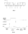
- FIG. 4 is a diagram illustrating a typical legacy interrupt map.
- FIG. 4 lists N interrupts (labeled 1 through N), sorted by priority, where interrupt 1 has the highest priority, and interrupt N has the lowest priority.
- the priorities of the interrupts are labeled 0 through N ⁇ 1, where the lowest numbers correspond to the highest priorities.
- FIG. 5 is a diagram illustrating an interrupt map, including two new interrupts used to trigger the stopping and starting of the processor.
- FIG. 5 lists the N legacy interrupts (labeled 1 through N). Two new interrupts (N+1 and N+2) are also shown. The new interrupts (N+1 and N+2) are re-mapped such that they have the highest priorities.
- interrupt N+1 has a priority of ⁇ 1, which is higher than all of the normal, legacy interrupts.
- Interrupt N+1 can also be thought of as the “ ⁇ 1 interrupt”.
- interrupt N+1 triggers a shut down interrupt routine (described below) and is generated prior to radio use.
- Interrupt N+2 has a priority of ⁇ 2, which is higher than all of the normal, legacy interrupts, as well as interrupt N+1. Interrupt N+2 can be thought of as the “ ⁇ 2 interrupt”.
- interrupt N+2 triggers a restart interrupt routine (described below) and is generated after radio use. Note that the terms “ ⁇ 1 interrupt” and “ ⁇ 2 interrupt” are merely just convenient names given to the interrupts and that other nomenclature can be used, as desired. Generally, the two new interrupts are configured to have a higher priority than all of the legacy interrupts.
- FIG. 6 is a flowchart illustrating the operation of the present invention.
- the process begins with step 6 - 10 , where one or more interrupts are generated and received by the interrupt controller. Generally, as interrupts are received, the interrupt controller will make a decision as to the next processing step that the processor will take. If multiple interrupts are received, the interrupt with the highest priority will be serviced first.
- the process determines whether a shut down interrupt (e.g., the ⁇ 1 interrupt described above) was received. If not (i.e., a normal, legacy interrupt was received), the process proceeds to step 6 - 14 , where the new interrupt is processed.
- a shut down interrupt e.g., the ⁇ 1 interrupt described above
- step 6 - 12 it was determined that a shut down interrupt ( ⁇ 1 interrupt) was received (i.e., usage of RF circuitry is about to start), then the process proceeds to step 6 - 16 , where the shut down interrupt service routine is processed.
- a shut down interrupt ⁇ 1 interrupt
- FIG. 7 illustrates one embodiment of a shut down interrupt service routine.
- the process waits for a restart interrupt (the ⁇ 2 interrupt).
- the ⁇ 2 interrupt is unmaskable, so the interrupt can not be masked within the interrupt controller.
- the process proceeds to step 6 - 20 , where the restart interrupt service routine is processed.
- FIG. 8 illustrates one embodiment of a restart interrupt service routine.
- a timer can be used to trigger the restart process, since the length of the RF time-slot should be known.
- a timer could be used to determine when a burst begins, or can be used to trigger the ⁇ 1 interrupt.
- FIG. 7 illustrates an embodiment of the reception of a shut down interrupt and a shut down interrupt service routine.
- the main purpose of the shut down interrupt service routine is to quickly transition the processor to a known stable state.
- the process begins at step 7 - 10 where the shut down interrupt was received.
- the ability to generate lower priority interrupts e.g., the normal, legacy interrupts 1 -N shown in FIG. 4 .
- the purpose of this step is to prevent additional interrupts from being sent to the processor while the radio is being used, causing the processor restart unexpectedly.
- any unneeded buses may be idled.
- the ability to access memory e.g., RAM
- any peripheral devices that are not designed to operate during use of the radio can be isolated from the processor. Isolating peripheral devices from the processor can be achieved in response to the shut down interrupt, or can be achieved separately from the process outlined in FIG. 7 . Examples of techniques for idling a bus and isolating peripheral devices are described in U.S. patent application Ser. No. 10/814,426, filed on Mar. 31, 2004, titled “COMMUNICATION APPARATUS IMPLEMENTING TIME DOMAIN ISOLATION WITH RESTRICTED BUS ACCESS”, which is incorporated by reference herein.
- the processor finishes any processing needed to prepare for radio use.
- the processor is instructed to wait for an interrupt.
- the wait for interrupt instruction is a general instruction that causes the processor to essentially stall until such time as an interrupt is received by the processor. Since no lower priority interrupt can be generated, the normal operations of the processor are stopped. In another example, the processor can be stalled by instructing the processor to wait for a bit to be set. The combination of these tasks results in a quiet processor environment.
- the processor clock can be disabled (step 7 - 20 ) without the need to precisely coordinate the clock stop time between the processor, the processor's bus, memories, and peripherals. This essentially decouples the clock stopping and starting from the processor stopping and starting.
- a clock signal can be disabled by gating a clock source.
- a clock signal can be disabled by removing the assertion of a clock enable from state holding elements. Note that the steps outlined in FIG. 7 may be performed in a different order, as desired. Also, not all of the steps are required, depending on the system, noise requirements, etc. Similarly, other steps could also be included in the process.
- a processor can be disabled by simply stopping the processor clock, and hoping that all is well when the clock signal returns. This method would seem to be less reliable than the method illustrated in FIG. 7 .
- the code is in the correct function to stop the processor at precisely the right time to stop the processor in the same manner described, through the use of the wait for interrupt instruction.
- the method relies on the tasks executed on the processor to be synchronized to the network timebase. While this method would work, a new software protocol may be desired for implementation. If the use of a simple clock stop is attempted, it would be possible to have synchronization of all clock domains to ensure that no domain received additional clocks relative to the others.
- FIG. 8 illustrates an embodiment of the reception of a restart interrupt and a restart interrupt service routine.
- the main purpose of the restart interrupt service routine is to restart the processor as quickly as possible. Since the processor has been instructed to wait for an interrupt, and the general purpose interrupts are disabled, then the processor will wait until the restart interrupt is received.
- the process begins at step 8 - 10 , where the restart interrupt is received.
- the processor clock is enabled, and clocking is restored to the internal circuitry of the processor.
- any desired processing is performed prior to returning to normal operation.
- the processor may perform data movement operations that may be desired to satisfy peripheral data movement needs.
- any disabled buses may be enabled. Also, full memory access may be enabled.
- the peripheral devices are enabled at this time to use system resources.
- the general interrupts are enabled.
- the context is restored to the normal system task that was running immediately prior to the radio use interrupts. Note that the steps outlined in FIG. 8 may be performed in a different order, as desired. Also, not all of the steps are desired, depending on the system, noise requirements, etc. Similarly, other steps could also be included in the process.
- FIG. 9 shows an example of a GSM data frame 70 and the relative timing of the shut down and restart interrupts.
- Frame 70 includes 8 slots, which may correspond to bursts of data.
- slot 2 represents a receive slot
- slot 4 is a monitor slot
- slot 6 constitutes a transmit slot.
- the remaining slots are unused for RF activity.
- the transmit, receive, and monitor slots could also be in different positions.
- the GSM slots 2 , 4 , and 6 are RF time-slots, with the remaining slots, in the context of this example, being signal-processing time-slots.
- FIG. 9 also shows the relative timing of the ⁇ 1 and ⁇ 2 interrupts (a more detailed view of the relative timing of the ⁇ 1 and ⁇ 2 interrupts is shown in FIG. 10 ).
- the ⁇ 1 interrupt is generated slightly before the beginning of each RF time-slot, due to the time used to process the shut down interrupt service routine (see FIG. 7 ).
- the ⁇ 2 interrupt is generated after the end of each RF time-slot to restart the processor.
- the precise timing of the interrupts can vary, as desired.
- FIG. 10 is a timing diagram illustrating the system operation context for an RF time-slot. Note that the diagram in FIG. 10 is not to scale, and is used to merely to illustrate the relative timing of the various items shown.
- the top line represents the wait for interrupt state, which begins during the shut down interrupt service routine (step 7 - 18 of FIG. 7 ) and ends when the ⁇ 2 restart interrupt is received (step 8 - 10 of FIG. 8 ).
- the system processes normal, legacy tasks.
- the ⁇ 2 interrupt the RF circuitry is in use, and the ⁇ 1 handler puts the processor in a sleep-like state.
- the ⁇ 2 interrupt initiates the ⁇ 2 handler, which restarts the processor. Part of the function of the ⁇ 2 handler is to end the ⁇ 1 handler.
- the system again processes normal, legacy tasks.
- the present invention may include additional features. For example, during times where it may be desirable to shut down a DSP, an apparatus may be receiving information for the DSP to process. In a mobile telephone apparatus, for example, the apparatus may receive RF signals while the RF circuitry (e.g., transceiver) is operating and the DSP is disabled. Sources that provide data to the DSP, or receive data from the DSP, may continue to have data needs that may need to be processed while the DSP is shut down. Therefore, a system using the present invention should manage the data, where needed. Following is a detailed description of an embodiment of the present invention applied to a DSP.
- the RF circuitry e.g., transceiver
- FIG. 11 is a block diagram of an interrupt control system 80 .
- the system 80 includes a digital signal processor (DSP) 82 .
- the DSP 82 is coupled to an interrupt controller 84 by lines 86 .
- Each of the lines 86 is coupled to one of the interrupt inputs INT 0 , INT 1 , and INT 2 of the DSP 82 .
- the interrupt inputs described are merely examples, and other configurations and notations may also be used.
- a system timer 88 is coupled to the interrupt controller 84 .
- the system timer 88 acts as a sequencer, or interrupt generator for generating interrupts for the interrupt controller 84 .
- the system timer 88 is the same system timer that is used with other parts of the apparatus (e.g., the system timer 56 shown in FIG. 3 ).
- the system timer 88 is separate.
- the interrupt controller 84 may also be coupled to one or more peripheral devices 90 , which may also generate interrupts for the interrupt controller 84 .
- FIG. 11 also shows clock management logic 92 coupled to the DSP 82 .
- the clock management logic 92 provides a clock signal to the DSP 82 , which, when disabled, will disable the DSP 82 , forcing the DSP 82 into a low noise mode. Connections between the DSP 82 , clock management logic 92 , and the interrupt controller 84 , allow the DSP 82 to configure each device.
- An RF input (RF IN) is coupled to the DSP 82 to provide a source of RF input signals (e.g., from RF front end circuitry, not shown).
- interrupts can be generated by the system timer 88 , as well as by other devices (e.g., peripheral devices 90 ). Interrupts from the system timer 88 are provided to the interrupt controller 84 via lines 100 , 102 , and 104 . In one example, line 100 is used to send the shut down interrupt, line 102 is used to send the restart interrupt, and line 104 is used to send other interrupts (e.g., legacy interrupts). When one or more interrupts are received by the interrupt controller 84 , interrupts are passed on to the DSP 82 via lines 86 . In one example, the interrupt input INT 0 is used for the shut down and restart interrupts.
- the interrupt inputs INT 1 and INT 2 are used for other, lower priority interrupts.
- the DSP 82 is configured such that interrupts received at input INT 0 have the highest priority, interrupts received at input INT 1 have the next highest priority, and interrupts received at input INT 2 have the lowest priority.
- interrupts received at input INT 0 have the highest priority
- interrupts received at input INT 1 have the next highest priority
- interrupts received at input INT 2 have the lowest priority.
- the DSP 82 uses a single interrupt input to receive all interrupts from the interrupt controller 84 .
- the present invention can efficiently stop and start a DSP by (1) providing a way to trigger a transition; and (2) providing procedures to efficiently stop and start the DSP.
- a transition is triggered by generating and servicing an interrupt of relatively high priority.
- the DSP is stopped or started such that the processor can operate in a normal, processing mode, and in a low noise, low power mode.
- the present invention configures a first interrupt (the shut down or “ ⁇ 1” interrupt) of relatively high priority that will be generated when the DSP is to be stopped (i.e., immediately before radio use).
- a second interrupt (the restart or “ ⁇ 2” interrupt) of relatively high priority is configured that will be generated when the DSP is to be restarted (i.e., immediately after radio use).
- interrupts can be prioritized as follows: the shut down and restart interrupts have the highest priority; legacy system timer interrupts have the next highest priority; and other peripheral interrupts have the lowest priority.
- the ⁇ 1 and ⁇ 2 interrupts described above for use in disabling the MCU 42 , and the ⁇ 1 and ⁇ 2 interrupts for use in disabling the DSP 82 are generated separately in one example, since the timing requirements (e.g., the desired preprocessing, etc.) may be different for the MCU 42 and the DSP 82 . In another example, the ⁇ 1 and ⁇ 2 interrupts can be the same, as desired.
- FIG. 12 is a flowchart illustrating one example of the operation of the present invention illustrated in FIG. 11 .
- the process begins with step 12 - 10 , where one or more interrupts are generated and received by the interrupt controller 84 .
- the interrupt controller will make a decision as to the next processing step that the DSP will take. If multiple interrupts are received, the interrupt with the highest priority will be serviced first. Also, if a shut down or restart interrupt is received, it is sent to the DSP 82 via input INT 0 , in the example shown in FIG. 11 .
- the process determines whether a shut down interrupt (e.g., the ⁇ 1 interrupt described above) was received from the system timer 88 .
- a shut down interrupt e.g., the ⁇ 1 interrupt described above
- step 12 - 14 the new interrupt is processed. In the case where a previously received higher priority interrupt has not yet been completed, this processing is continued. Note that while processing interrupts at step 12 - 14 , the interrupt processing can be preempted by the reception of a higher interrupt. The process then goes back to step 12 - 10 . Note that, between received interrupts, the DSP is performing general processing tasks.
- shut down interrupt service routine begins.
- the ability to generate lower priority interrupts is disabled. The purpose of this step is to prevent additional interrupts from being sent to the DSP while the radio is being used, causing the DSP restart unexpectedly.
- the DSP 82 finishes any desired processing needed to prepare for radio use.
- the DSP 82 may perform preprocessing to the DSP and the DSP peripherals. For example, the DSP 82 may flush the audio buffer and set up the system for managing RF signals while the DSP 82 is disabled.
- the DSP 82 configures the restart interrupt as the source to re-activate the DSP clock.
- the DSP clock is disabled via the clock management logic 92 .
- the system waits for the restart interrupt (the ⁇ 2 interrupt).
- the restart interrupt the ⁇ 2 interrupt.
- any other interrupts that might be generated e.g., from peripheral devices 90
- the masking of interrupts is configured to let the restart interrupt through.
- the DSP 82 can be configured to process signals at a faster rate than it would need to if it were never disabled. In one example, the DSP 82 is configured to process signals at a data rate which is greater than the rate at which the data is generated.
- the restart interrupt service routine is processed.
- the restart interrupt is generated by the system timer 88
- the interrupt is received by the clock management logic 92 , which will then enable the DSP clock (step 12 - 26 ).
- the DSP performs post-processing to the DSP and DSP peripherals.
- the present invention can be implemented in many ways to provide various advantages.
- One novel advantage of the present invention is that the invention provides a processor able to minimize noise created by digital circuitry.
- Another advantage of the present invention is the provision of the ability to quickly transition from high performance processing to low noise modes and back, with a minimum amount of overhead. In addition, the low noise modes cannot be accidentally exited, although it could be exited earlier than originally expected.
Abstract
Description
Claims (26)
Priority Applications (10)
| Application Number | Priority Date | Filing Date | Title |
|---|---|---|---|
| US10/955,926 US7433393B2 (en) | 2004-07-23 | 2004-09-30 | Apparatus for controlling a digital signal processor for radio isolation and associated methods |
| TW094133300A TWI286419B (en) | 2004-09-30 | 2005-09-26 | Apparatus for controlling a digital signal processor for radio isolation and associated methods |
| ES05803663T ES2341018T3 (en) | 2004-09-30 | 2005-09-30 | APPARATUS FOR CONTROLLING A DIGITAL SIGNAL PROCESSOR FOR RADIO INSULATION AND ASSOCIATED METHODS. |
| DE602005020328T DE602005020328D1 (en) | 2004-09-30 | 2005-09-30 | DEVICE FOR CONTROLLING A DIGITAL SIGNAL PROCESSOR FOR RADIO INSULATION AND ASSOCIATED METHODS |
| AT05803663T ATE463003T1 (en) | 2004-09-30 | 2005-09-30 | DEVICE FOR CONTROLLING A DIGITAL SIGNAL PROCESSOR FOR RADIO ISOLATION AND ASSOCIATED METHOD |
| PCT/US2005/035279 WO2006039544A1 (en) | 2004-09-30 | 2005-09-30 | Apparatus for controlling a digital signal processor for radio isolation and associated methods |
| EP05803663A EP1800202B1 (en) | 2004-09-30 | 2005-09-30 | Apparatus for controlling a digital signal processor for radio isolation and associated methods |
| JP2007534816A JP2008515355A (en) | 2004-09-30 | 2005-09-30 | Apparatus and related method for controlling a digital signal processor for radio isolation |
| KR1020077008272A KR20070093392A (en) | 2004-09-30 | 2005-09-30 | Apparatus for controlling a digital signal processor for radio isolation and associated methods |
| CNB2005800407568A CN100568155C (en) | 2004-09-30 | 2005-09-30 | Control is used for the device and the correlation technique of the digital signal processor of radio isolation |
Applications Claiming Priority (2)
| Application Number | Priority Date | Filing Date | Title |
|---|---|---|---|
| US10/898,057 US20050008095A1 (en) | 2004-07-23 | 2004-07-23 | Apparatus using interrupts for controlling a processor for radio isolation and associated methods |
| US10/955,926 US7433393B2 (en) | 2004-07-23 | 2004-09-30 | Apparatus for controlling a digital signal processor for radio isolation and associated methods |
Related Parent Applications (1)
| Application Number | Title | Priority Date | Filing Date |
|---|---|---|---|
| US10/898,057 Continuation-In-Part US20050008095A1 (en) | 2004-07-23 | 2004-07-23 | Apparatus using interrupts for controlling a processor for radio isolation and associated methods |
Publications (2)
| Publication Number | Publication Date |
|---|---|
| US20060018372A1 US20060018372A1 (en) | 2006-01-26 |
| US7433393B2 true US7433393B2 (en) | 2008-10-07 |
Family
ID=35546463
Family Applications (1)
| Application Number | Title | Priority Date | Filing Date |
|---|---|---|---|
| US10/955,926 Active 2026-08-03 US7433393B2 (en) | 2004-07-23 | 2004-09-30 | Apparatus for controlling a digital signal processor for radio isolation and associated methods |
Country Status (10)
| Country | Link |
|---|---|
| US (1) | US7433393B2 (en) |
| EP (1) | EP1800202B1 (en) |
| JP (1) | JP2008515355A (en) |
| KR (1) | KR20070093392A (en) |
| CN (1) | CN100568155C (en) |
| AT (1) | ATE463003T1 (en) |
| DE (1) | DE602005020328D1 (en) |
| ES (1) | ES2341018T3 (en) |
| TW (1) | TWI286419B (en) |
| WO (1) | WO2006039544A1 (en) |
Cited By (1)
| Publication number | Priority date | Publication date | Assignee | Title |
|---|---|---|---|---|
| US8472990B2 (en) | 2004-07-23 | 2013-06-25 | St Ericsson Sa | Apparatus using interrupts for controlling a processor for radio isolation and associated method |
Families Citing this family (7)
| Publication number | Priority date | Publication date | Assignee | Title |
|---|---|---|---|---|
| US7729664B2 (en) * | 2006-04-20 | 2010-06-01 | Palm, Inc. | Technique for reducing interference to radio operations on a computing device |
| JP5578811B2 (en) * | 2009-06-30 | 2014-08-27 | キヤノン株式会社 | Information processing apparatus, information processing apparatus control method, and program |
| JP5814542B2 (en) * | 2010-12-06 | 2015-11-17 | 株式会社東芝 | Oscillator circuit |
| US20140052532A1 (en) * | 2012-08-17 | 2014-02-20 | Google Inc. | Portable device wireless reader and payment transaction terminal functionality with other portable devices |
| US9819424B2 (en) * | 2013-09-09 | 2017-11-14 | Apple Inc. | Method and apparatus to mitigate interference between hardware circuitry and wireless circuitry in a wireless communication device |
| CN105446798A (en) * | 2014-07-31 | 2016-03-30 | 展讯通信(上海)有限公司 | Multi-core processing system and method, and mobile terminal |
| JP7124038B2 (en) | 2020-11-16 | 2022-08-23 | 株式会社東芝 | Communication device, communication method and program |
Citations (56)
| Publication number | Priority date | Publication date | Assignee | Title |
|---|---|---|---|---|
| US4384361A (en) | 1979-09-29 | 1983-05-17 | Nippon Electric Co., Ltd. | Selective calling receiver |
| US4805165A (en) | 1986-03-24 | 1989-02-14 | Iwatsu Electric Co., Ltd. | Time division multiplex data transmission method and apparatus |
| US4870699A (en) | 1986-03-26 | 1989-09-26 | General Electric Company | Method and apparatus for controlling the frequency of operation and at least one further variable operating parameter of a radio communications device |
| US4879758A (en) | 1987-01-02 | 1989-11-07 | Motorola, Inc. | Communication receiver system having a decoder operating at variable frequencies |
| US4930126A (en) | 1989-06-05 | 1990-05-29 | Motorola, Inc. | Time division multiplex system suited for burst analog transmission |
| US4996639A (en) | 1987-11-27 | 1991-02-26 | Nec Corporation | Data processor including an A/D converter for converting a plurality of analog input channels into digital data |
| US5031233A (en) | 1989-07-11 | 1991-07-09 | At&E Corporation | Single chip radio receiver with one off-chip filter |
| EP0447302A1 (en) | 1990-03-16 | 1991-09-18 | Matra Communication | Time-multiplexed radio communication device |
| US5058203A (en) | 1988-05-21 | 1991-10-15 | Fujitsu Limited | Mobile telephone terminal having selectively used processor unit for low power consumption |
| EP0463621A1 (en) | 1990-06-28 | 1992-01-02 | Firma Erika Köchler | Receiver for digital radio signals |
| US5142699A (en) | 1988-07-15 | 1992-08-25 | Nec Corporation | Radio receiver with clock signal controlled to improve the signal to noise ratio |
| US5150361A (en) | 1989-01-23 | 1992-09-22 | Motorola, Inc. | Energy saving protocol for a TDM radio |
| US5151769A (en) | 1991-04-04 | 1992-09-29 | General Electric Company | Optically patterned RF shield for an integrated circuit chip for analog and/or digital operation at microwave frequencies |
| EP0511511A2 (en) | 1991-04-30 | 1992-11-04 | Motorola Israel Limited | Microprocessor controlled electronic equipment |
| US5212796A (en) * | 1990-01-02 | 1993-05-18 | Motorola, Inc. | System with modules using priority numbers related to interrupt vectors for bit-serial-arbitration on independent arbitration bus while CPU executing instructions |
| US5241541A (en) | 1990-03-15 | 1993-08-31 | International Business Machines Corporation | Burst time division multiplex interface for integrated data link controller |
| US5280644A (en) | 1992-12-22 | 1994-01-18 | Motorola, Inc. | Frequency control circuit, and associated method, for a receiver operative to receive signals-transmitted thereto in intermittent bursts |
| US5307066A (en) | 1990-06-11 | 1994-04-26 | Oki Electric Industry Co., Ltd. | Microprocessor controlled converter having reduced noise interference and method of operating same |
| US5355524A (en) | 1992-01-21 | 1994-10-11 | Motorola, Inc. | Integrated radio receiver/transmitter structure |
| US5448755A (en) | 1991-05-07 | 1995-09-05 | Matsushita Electric Industrial Co., Ltd. | Oscillation scheme for a selective calling reception apparatus |
| US5471471A (en) | 1992-01-03 | 1995-11-28 | Motorola, Inc. | Signal communication method and apparatus |
| US5471663A (en) | 1993-07-01 | 1995-11-28 | Motorola, Inc. | Expanded microcomputer system for controlling radio frequency interference |
| US5475684A (en) | 1994-01-25 | 1995-12-12 | Nec Corporation | Time-division multiplex communication transmission apparatus |
| US5487181A (en) | 1992-10-28 | 1996-01-23 | Ericsson Ge Mobile Communications Inc. | Low power architecture for portable and mobile two-way radios |
| US5519711A (en) | 1993-11-22 | 1996-05-21 | Nokia Mobile Phones Ltd. | Switch-mode power supply for time division multiple access radio phone systems |
| US5604928A (en) | 1992-01-31 | 1997-02-18 | Canon Kabushiki Kaisha | Portable electronic device with radio communication and controlled computer status |
| US5630224A (en) | 1994-12-29 | 1997-05-13 | Motorola, Inc. | Method and apparatus for avoiding desensitization of a radio frequency receiver |
| US5649160A (en) | 1995-05-23 | 1997-07-15 | Microunity Systems Engineering, Inc. | Noise reduction in integrated circuits and circuit assemblies |
| US5758278A (en) | 1995-02-07 | 1998-05-26 | Nokia Mobile Phones Limited | Method and apparatus for periodically re-activating a mobile telephone system clock prior to receiving polling signals |
| US5764693A (en) | 1994-11-14 | 1998-06-09 | Research In Motion Limited | Wireless radio modem with minimal inter-device RF interference |
| US5812936A (en) | 1995-09-19 | 1998-09-22 | Lucent Technologies, Inc. | Energy-efficient time-division radio that reduces the induction of baseband interference |
| US5838741A (en) | 1997-02-10 | 1998-11-17 | Motorola, Inc. | Communication device and method for reducing effects of noise introduction by synchronizing data transfer to a received signal |
| US5842037A (en) | 1995-03-20 | 1998-11-24 | Telefonaktiebolaget Lm Ericsson | Interference reduction in TDM-communication/computing devices |
| US5859883A (en) | 1989-08-14 | 1999-01-12 | Interdigital Technology Corporation | Subscriber unit for wireless digital subscriber communication system |
| US5872540A (en) | 1997-06-26 | 1999-02-16 | Electro-Radiation Incorporated | Digital interference suppression system for radio frequency interference cancellation |
| US5875449A (en) | 1995-08-10 | 1999-02-23 | Nec Corporation | Computer connection available data wireless apparatus with clock signal frequency variable function |
| US5917854A (en) | 1994-11-14 | 1999-06-29 | Research In Motion Limited | Wireless radio modem with minimal interdevice RF interference |
| US5920592A (en) | 1996-03-13 | 1999-07-06 | Nec Corporation | Data transmitter-receiver |
| US5923761A (en) | 1996-05-24 | 1999-07-13 | Lsi Logic Corporation | Single chip solution for multimedia GSM mobile station systems |
| EP0939495A1 (en) | 1998-02-26 | 1999-09-01 | Motorola Semiconducteurs S.A. | Power saving for a electronic devices |
| US5953640A (en) | 1997-04-30 | 1999-09-14 | Motorola, Inc. | Configuration single chip receiver integrated circuit architecture |
| US6020614A (en) | 1998-03-25 | 2000-02-01 | Worley; Eugene Robert | Method of reducing substrate noise coupling in mixed signal integrated circuits |
| WO2001039406A2 (en) | 1999-11-25 | 2001-05-31 | Siemens Aktiengesellschaft | Method for effecting the interference-reduced operation of a radio transceiver and a radio transceiver |
| US6243597B1 (en) | 1997-10-24 | 2001-06-05 | U.S. Philips Corporation | Battery-operated communications device with the continuously running reference clock of which the frequency is reduced when a synchronization unit is controlled during a stand-by mode |
| US6246335B1 (en) | 1993-12-28 | 2001-06-12 | Nec Corporation | Portable information equipment system and control method thereof |
| US6366622B1 (en) | 1998-12-18 | 2002-04-02 | Silicon Wave, Inc. | Apparatus and method for wireless communications |
| US20020080728A1 (en) | 2000-11-03 | 2002-06-27 | Sugar Gary L. | Wideband multi-protocol wireless radio transceiver system |
| US6442407B1 (en) | 1997-08-02 | 2002-08-27 | Koninklijke Philips Electronics N.V. | Mobile radio telephone set |
| US6480553B1 (en) | 1998-04-23 | 2002-11-12 | Winbond Electronics Corp. | Gaussian frequency-shift keying transciever for ISM wideband communication |
| US6498819B1 (en) | 1998-10-19 | 2002-12-24 | Motorola, Inc. | Integrated multi-mode bandpass sigma-delta receiver subsystem with interference mitigation and method of using same |
| US6510185B2 (en) | 1998-07-24 | 2003-01-21 | Gct Semiconductor, Inc. | Single chip CMOS transmitter/receiver |
| US20030020521A1 (en) | 1998-07-24 | 2003-01-30 | Gct Semiconductor, Inc. | Single chip CMOS transmitter/receiver and method of using same |
| US20040116168A1 (en) | 2002-12-11 | 2004-06-17 | Nec Corporation | Cellular phone suppressing degradation of receiving sensitivity |
| US20040120435A1 (en) | 2002-12-09 | 2004-06-24 | Baoguo Yang | Pipeline architecture for multi-slot wireless link processing |
| US20040146030A1 (en) | 2003-01-23 | 2004-07-29 | Yu-Cheng Hsieh | Method for switching a time frame based mobile unit to a sleep mode |
| US6963554B1 (en) * | 2000-12-27 | 2005-11-08 | National Semiconductor Corporation | Microwire dynamic sequencer pipeline stall |
Family Cites Families (4)
| Publication number | Priority date | Publication date | Assignee | Title |
|---|---|---|---|---|
| JPH11112442A (en) * | 1997-10-08 | 1999-04-23 | Nec Corp | Radio communication terminal |
| JP3241332B2 (en) * | 1998-10-27 | 2001-12-25 | 日本電気株式会社 | Noise reduction method for wireless portable terminal |
| JP4167349B2 (en) * | 1999-05-20 | 2008-10-15 | 新潟精密株式会社 | Receiving machine |
| JP2002076267A (en) * | 2000-08-22 | 2002-03-15 | Hitachi Ltd | Radio transmitter |
-
2004
- 2004-09-30 US US10/955,926 patent/US7433393B2/en active Active
-
2005
- 2005-09-26 TW TW094133300A patent/TWI286419B/en active
- 2005-09-30 EP EP05803663A patent/EP1800202B1/en not_active Not-in-force
- 2005-09-30 DE DE602005020328T patent/DE602005020328D1/en active Active
- 2005-09-30 JP JP2007534816A patent/JP2008515355A/en active Pending
- 2005-09-30 AT AT05803663T patent/ATE463003T1/en not_active IP Right Cessation
- 2005-09-30 CN CNB2005800407568A patent/CN100568155C/en not_active Expired - Fee Related
- 2005-09-30 KR KR1020077008272A patent/KR20070093392A/en not_active Application Discontinuation
- 2005-09-30 WO PCT/US2005/035279 patent/WO2006039544A1/en active Application Filing
- 2005-09-30 ES ES05803663T patent/ES2341018T3/en active Active
Patent Citations (60)
| Publication number | Priority date | Publication date | Assignee | Title |
|---|---|---|---|---|
| US4384361A (en) | 1979-09-29 | 1983-05-17 | Nippon Electric Co., Ltd. | Selective calling receiver |
| US4805165A (en) | 1986-03-24 | 1989-02-14 | Iwatsu Electric Co., Ltd. | Time division multiplex data transmission method and apparatus |
| US4870699A (en) | 1986-03-26 | 1989-09-26 | General Electric Company | Method and apparatus for controlling the frequency of operation and at least one further variable operating parameter of a radio communications device |
| US4879758A (en) | 1987-01-02 | 1989-11-07 | Motorola, Inc. | Communication receiver system having a decoder operating at variable frequencies |
| US4996639A (en) | 1987-11-27 | 1991-02-26 | Nec Corporation | Data processor including an A/D converter for converting a plurality of analog input channels into digital data |
| US5058203A (en) | 1988-05-21 | 1991-10-15 | Fujitsu Limited | Mobile telephone terminal having selectively used processor unit for low power consumption |
| US5142699A (en) | 1988-07-15 | 1992-08-25 | Nec Corporation | Radio receiver with clock signal controlled to improve the signal to noise ratio |
| US5150361A (en) | 1989-01-23 | 1992-09-22 | Motorola, Inc. | Energy saving protocol for a TDM radio |
| US4930126A (en) | 1989-06-05 | 1990-05-29 | Motorola, Inc. | Time division multiplex system suited for burst analog transmission |
| US5031233A (en) | 1989-07-11 | 1991-07-09 | At&E Corporation | Single chip radio receiver with one off-chip filter |
| US5859883A (en) | 1989-08-14 | 1999-01-12 | Interdigital Technology Corporation | Subscriber unit for wireless digital subscriber communication system |
| US5212796A (en) * | 1990-01-02 | 1993-05-18 | Motorola, Inc. | System with modules using priority numbers related to interrupt vectors for bit-serial-arbitration on independent arbitration bus while CPU executing instructions |
| US5241541A (en) | 1990-03-15 | 1993-08-31 | International Business Machines Corporation | Burst time division multiplex interface for integrated data link controller |
| EP0447302B1 (en) | 1990-03-16 | 1994-05-18 | Matra Communication | Time-multiplexed radio communication device |
| EP0447302A1 (en) | 1990-03-16 | 1991-09-18 | Matra Communication | Time-multiplexed radio communication device |
| US5307066A (en) | 1990-06-11 | 1994-04-26 | Oki Electric Industry Co., Ltd. | Microprocessor controlled converter having reduced noise interference and method of operating same |
| EP0463621B1 (en) | 1990-06-28 | 2000-01-19 | Firma Erika Köchler | Receiver for digital radio signals |
| EP0463621A1 (en) | 1990-06-28 | 1992-01-02 | Firma Erika Köchler | Receiver for digital radio signals |
| US5151769A (en) | 1991-04-04 | 1992-09-29 | General Electric Company | Optically patterned RF shield for an integrated circuit chip for analog and/or digital operation at microwave frequencies |
| EP0511511A2 (en) | 1991-04-30 | 1992-11-04 | Motorola Israel Limited | Microprocessor controlled electronic equipment |
| EP0511511B1 (en) | 1991-04-30 | 1996-12-11 | Motorola Israel Limited | Microprocessor controlled electronic equipment |
| US5448755A (en) | 1991-05-07 | 1995-09-05 | Matsushita Electric Industrial Co., Ltd. | Oscillation scheme for a selective calling reception apparatus |
| US5471471A (en) | 1992-01-03 | 1995-11-28 | Motorola, Inc. | Signal communication method and apparatus |
| US5355524A (en) | 1992-01-21 | 1994-10-11 | Motorola, Inc. | Integrated radio receiver/transmitter structure |
| US5604928A (en) | 1992-01-31 | 1997-02-18 | Canon Kabushiki Kaisha | Portable electronic device with radio communication and controlled computer status |
| US5487181A (en) | 1992-10-28 | 1996-01-23 | Ericsson Ge Mobile Communications Inc. | Low power architecture for portable and mobile two-way radios |
| US5280644A (en) | 1992-12-22 | 1994-01-18 | Motorola, Inc. | Frequency control circuit, and associated method, for a receiver operative to receive signals-transmitted thereto in intermittent bursts |
| US5471663A (en) | 1993-07-01 | 1995-11-28 | Motorola, Inc. | Expanded microcomputer system for controlling radio frequency interference |
| US5519711A (en) | 1993-11-22 | 1996-05-21 | Nokia Mobile Phones Ltd. | Switch-mode power supply for time division multiple access radio phone systems |
| US6246335B1 (en) | 1993-12-28 | 2001-06-12 | Nec Corporation | Portable information equipment system and control method thereof |
| US5475684A (en) | 1994-01-25 | 1995-12-12 | Nec Corporation | Time-division multiplex communication transmission apparatus |
| US5764693A (en) | 1994-11-14 | 1998-06-09 | Research In Motion Limited | Wireless radio modem with minimal inter-device RF interference |
| US5917854A (en) | 1994-11-14 | 1999-06-29 | Research In Motion Limited | Wireless radio modem with minimal interdevice RF interference |
| US5630224A (en) | 1994-12-29 | 1997-05-13 | Motorola, Inc. | Method and apparatus for avoiding desensitization of a radio frequency receiver |
| US5758278A (en) | 1995-02-07 | 1998-05-26 | Nokia Mobile Phones Limited | Method and apparatus for periodically re-activating a mobile telephone system clock prior to receiving polling signals |
| US5842037A (en) | 1995-03-20 | 1998-11-24 | Telefonaktiebolaget Lm Ericsson | Interference reduction in TDM-communication/computing devices |
| US5649160A (en) | 1995-05-23 | 1997-07-15 | Microunity Systems Engineering, Inc. | Noise reduction in integrated circuits and circuit assemblies |
| US5875449A (en) | 1995-08-10 | 1999-02-23 | Nec Corporation | Computer connection available data wireless apparatus with clock signal frequency variable function |
| US5812936A (en) | 1995-09-19 | 1998-09-22 | Lucent Technologies, Inc. | Energy-efficient time-division radio that reduces the induction of baseband interference |
| US5920592A (en) | 1996-03-13 | 1999-07-06 | Nec Corporation | Data transmitter-receiver |
| US5923761A (en) | 1996-05-24 | 1999-07-13 | Lsi Logic Corporation | Single chip solution for multimedia GSM mobile station systems |
| US5838741A (en) | 1997-02-10 | 1998-11-17 | Motorola, Inc. | Communication device and method for reducing effects of noise introduction by synchronizing data transfer to a received signal |
| US5953640A (en) | 1997-04-30 | 1999-09-14 | Motorola, Inc. | Configuration single chip receiver integrated circuit architecture |
| US5872540A (en) | 1997-06-26 | 1999-02-16 | Electro-Radiation Incorporated | Digital interference suppression system for radio frequency interference cancellation |
| US6442407B1 (en) | 1997-08-02 | 2002-08-27 | Koninklijke Philips Electronics N.V. | Mobile radio telephone set |
| US6243597B1 (en) | 1997-10-24 | 2001-06-05 | U.S. Philips Corporation | Battery-operated communications device with the continuously running reference clock of which the frequency is reduced when a synchronization unit is controlled during a stand-by mode |
| EP0939495A1 (en) | 1998-02-26 | 1999-09-01 | Motorola Semiconducteurs S.A. | Power saving for a electronic devices |
| US6020614A (en) | 1998-03-25 | 2000-02-01 | Worley; Eugene Robert | Method of reducing substrate noise coupling in mixed signal integrated circuits |
| US6480553B1 (en) | 1998-04-23 | 2002-11-12 | Winbond Electronics Corp. | Gaussian frequency-shift keying transciever for ISM wideband communication |
| US6510185B2 (en) | 1998-07-24 | 2003-01-21 | Gct Semiconductor, Inc. | Single chip CMOS transmitter/receiver |
| US20030020521A1 (en) | 1998-07-24 | 2003-01-30 | Gct Semiconductor, Inc. | Single chip CMOS transmitter/receiver and method of using same |
| US6498819B1 (en) | 1998-10-19 | 2002-12-24 | Motorola, Inc. | Integrated multi-mode bandpass sigma-delta receiver subsystem with interference mitigation and method of using same |
| US6366622B1 (en) | 1998-12-18 | 2002-04-02 | Silicon Wave, Inc. | Apparatus and method for wireless communications |
| WO2001039406A2 (en) | 1999-11-25 | 2001-05-31 | Siemens Aktiengesellschaft | Method for effecting the interference-reduced operation of a radio transceiver and a radio transceiver |
| US20020080728A1 (en) | 2000-11-03 | 2002-06-27 | Sugar Gary L. | Wideband multi-protocol wireless radio transceiver system |
| US6963554B1 (en) * | 2000-12-27 | 2005-11-08 | National Semiconductor Corporation | Microwire dynamic sequencer pipeline stall |
| US20040120435A1 (en) | 2002-12-09 | 2004-06-24 | Baoguo Yang | Pipeline architecture for multi-slot wireless link processing |
| US20040116168A1 (en) | 2002-12-11 | 2004-06-17 | Nec Corporation | Cellular phone suppressing degradation of receiving sensitivity |
| US7209767B2 (en) * | 2002-12-11 | 2007-04-24 | Nec Corporation | Cellular phone suppressing degradation of receiving sensitivity |
| US20040146030A1 (en) | 2003-01-23 | 2004-07-29 | Yu-Cheng Hsieh | Method for switching a time frame based mobile unit to a sleep mode |
Non-Patent Citations (2)
| Title |
|---|
| International Search Report for PCT/US05/35279, date of mailing, Jan. 27, 2006, 3 pages. |
| International Search Report for PCT/US2005/025909, dated of mailing: Nov. 15, 2005, 3 pages. |
Cited By (1)
| Publication number | Priority date | Publication date | Assignee | Title |
|---|---|---|---|---|
| US8472990B2 (en) | 2004-07-23 | 2013-06-25 | St Ericsson Sa | Apparatus using interrupts for controlling a processor for radio isolation and associated method |
Also Published As
| Publication number | Publication date |
|---|---|
| ES2341018T3 (en) | 2010-06-14 |
| CN101151586A (en) | 2008-03-26 |
| WO2006039544A1 (en) | 2006-04-13 |
| CN100568155C (en) | 2009-12-09 |
| US20060018372A1 (en) | 2006-01-26 |
| DE602005020328D1 (en) | 2010-05-12 |
| ATE463003T1 (en) | 2010-04-15 |
| KR20070093392A (en) | 2007-09-18 |
| EP1800202A1 (en) | 2007-06-27 |
| JP2008515355A (en) | 2008-05-08 |
| TWI286419B (en) | 2007-09-01 |
| EP1800202B1 (en) | 2010-03-31 |
| TW200629755A (en) | 2006-08-16 |
Similar Documents
| Publication | Publication Date | Title |
|---|---|---|
| US7380033B2 (en) | Communication apparatus implementing time domain isolation with restricted bus access | |
| EP1800202B1 (en) | Apparatus for controlling a digital signal processor for radio isolation and associated methods | |
| EP1784921B1 (en) | Apparatus using interrupt signals for controlling a processor for radio installation and associated method | |
| US5987556A (en) | Data processing device having accelerator for digital signal processing | |
| JP5002783B2 (en) | Communication device including dual timer unit | |
| US20130329617A1 (en) | Apparatus and methods for control of sleep modes in a transceiver | |
| US20200133910A1 (en) | Programmed delay for rffe bus triggers | |
| US7761056B2 (en) | Method of controlling a processor for radio isolation using a timer | |
| US8472990B2 (en) | Apparatus using interrupts for controlling a processor for radio isolation and associated method | |
| KR20070120939A (en) | Communication apparatus having a sim interface compatible with radio isolation | |
| US11275701B2 (en) | Secure timer synchronization between function block and external SOC | |
| US11907154B2 (en) | Latency and power efficient clock and data recovery in a high-speed one-wire bidirectional bus | |
| US20210081340A1 (en) | Controlling the application time of radio frequency front end triggers based on execution of sequences |
Legal Events
| Date | Code | Title | Description |
|---|---|---|---|
| AS | Assignment |
Owner name: SILICON LABORATORIES, INC., TEXAS Free format text: ASSIGNMENT OF ASSIGNORS INTEREST;ASSIGNORS:CHEN, SHAOJIE;RUSH, FREDERICK A.;VISHAKHADATTA, G. DIWAKAR;AND OTHERS;REEL/FRAME:015632/0956 Effective date: 20050121 |
|
| AS | Assignment |
Owner name: NXP, B.V.,NETHERLANDS Free format text: ASSIGNMENT OF ASSIGNORS INTEREST;ASSIGNOR:SILICON LABORATORIES, INC.;REEL/FRAME:019069/0526 Effective date: 20070323 Owner name: NXP, B.V., NETHERLANDS Free format text: ASSIGNMENT OF ASSIGNORS INTEREST;ASSIGNOR:SILICON LABORATORIES, INC.;REEL/FRAME:019069/0526 Effective date: 20070323 |
|
| STCF | Information on status: patent grant |
Free format text: PATENTED CASE |
|
| FPAY | Fee payment |
Year of fee payment: 4 |
|
| AS | Assignment |
Owner name: ST WIRELESS SA, SWITZERLAND Free format text: ASSIGNMENT OF ASSIGNORS INTEREST;ASSIGNOR:NXP B.V.;REEL/FRAME:037605/0983 Effective date: 20080805 |
|
| AS | Assignment |
Owner name: ST-ERICSSON SA, SWITZERLAND Free format text: CHANGE OF NAME;ASSIGNOR:ST WIRELESS SA;REEL/FRAME:037683/0128 Effective date: 20080714 Owner name: ST-ERICSSON SA, EN LIQUIDATION, SWITZERLAND Free format text: STATUS CHANGE-ENTITY IN LIQUIDATION;ASSIGNOR:ST-ERICSSON SA;REEL/FRAME:037739/0493 Effective date: 20150223 |
|
| FPAY | Fee payment |
Year of fee payment: 8 |
|
| AS | Assignment |
Owner name: OPTIS CIRCUIT TECHNOLOGY, LLC,, TEXAS Free format text: ASSIGNMENT OF ASSIGNORS INTEREST;ASSIGNOR:ST-ERICSSON SA, EN LIQUIDATION;REEL/FRAME:048504/0519 Effective date: 20160831 |
|
| AS | Assignment |
Owner name: TELEFONAKTIEBOLAGET L M ERICSSON (PUBL), SWEDEN Free format text: ASSIGNMENT OF ASSIGNORS INTEREST;ASSIGNOR:OPTIS CIRCUIT TECHNOLOGY, LLC,;REEL/FRAME:048529/0510 Effective date: 20181130 |
|
| MAFP | Maintenance fee payment |
Free format text: PAYMENT OF MAINTENANCE FEE, 12TH YEAR, LARGE ENTITY (ORIGINAL EVENT CODE: M1553); ENTITY STATUS OF PATENT OWNER: LARGE ENTITY Year of fee payment: 12 |