US7818477B2 - Storage device with buffer control unit - Google Patents
Storage device with buffer control unit Download PDFInfo
- Publication number
- US7818477B2 US7818477B2 US11/909,749 US90974906A US7818477B2 US 7818477 B2 US7818477 B2 US 7818477B2 US 90974906 A US90974906 A US 90974906A US 7818477 B2 US7818477 B2 US 7818477B2
- Authority
- US
- United States
- Prior art keywords
- data
- save
- buffer
- nonvolatile
- control information
- Prior art date
- Legal status (The legal status is an assumption and is not a legal conclusion. Google has not performed a legal analysis and makes no representation as to the accuracy of the status listed.)
- Expired - Fee Related, expires
Links
Images


Classifications
-
- G—PHYSICS
- G06—COMPUTING; CALCULATING OR COUNTING
- G06F—ELECTRIC DIGITAL DATA PROCESSING
- G06F3/00—Input arrangements for transferring data to be processed into a form capable of being handled by the computer; Output arrangements for transferring data from processing unit to output unit, e.g. interface arrangements
- G06F3/06—Digital input from, or digital output to, record carriers, e.g. RAID, emulated record carriers or networked record carriers
- G06F3/0601—Interfaces specially adapted for storage systems
- G06F3/0628—Interfaces specially adapted for storage systems making use of a particular technique
- G06F3/0655—Vertical data movement, i.e. input-output transfer; data movement between one or more hosts and one or more storage devices
- G06F3/0659—Command handling arrangements, e.g. command buffers, queues, command scheduling
-
- G—PHYSICS
- G06—COMPUTING; CALCULATING OR COUNTING
- G06F—ELECTRIC DIGITAL DATA PROCESSING
- G06F11/00—Error detection; Error correction; Monitoring
- G06F11/07—Responding to the occurrence of a fault, e.g. fault tolerance
- G06F11/14—Error detection or correction of the data by redundancy in operation
- G06F11/1402—Saving, restoring, recovering or retrying
- G06F11/1415—Saving, restoring, recovering or retrying at system level
- G06F11/1441—Resetting or repowering
-
- G—PHYSICS
- G06—COMPUTING; CALCULATING OR COUNTING
- G06F—ELECTRIC DIGITAL DATA PROCESSING
- G06F3/00—Input arrangements for transferring data to be processed into a form capable of being handled by the computer; Output arrangements for transferring data from processing unit to output unit, e.g. interface arrangements
- G06F3/06—Digital input from, or digital output to, record carriers, e.g. RAID, emulated record carriers or networked record carriers
- G06F3/0601—Interfaces specially adapted for storage systems
- G06F3/0602—Interfaces specially adapted for storage systems specifically adapted to achieve a particular effect
- G06F3/061—Improving I/O performance
-
- G—PHYSICS
- G06—COMPUTING; CALCULATING OR COUNTING
- G06F—ELECTRIC DIGITAL DATA PROCESSING
- G06F3/00—Input arrangements for transferring data to be processed into a form capable of being handled by the computer; Output arrangements for transferring data from processing unit to output unit, e.g. interface arrangements
- G06F3/06—Digital input from, or digital output to, record carriers, e.g. RAID, emulated record carriers or networked record carriers
- G06F3/0601—Interfaces specially adapted for storage systems
- G06F3/0628—Interfaces specially adapted for storage systems making use of a particular technique
- G06F3/0655—Vertical data movement, i.e. input-output transfer; data movement between one or more hosts and one or more storage devices
- G06F3/0656—Data buffering arrangements
-
- G—PHYSICS
- G06—COMPUTING; CALCULATING OR COUNTING
- G06F—ELECTRIC DIGITAL DATA PROCESSING
- G06F3/00—Input arrangements for transferring data to be processed into a form capable of being handled by the computer; Output arrangements for transferring data from processing unit to output unit, e.g. interface arrangements
- G06F3/06—Digital input from, or digital output to, record carriers, e.g. RAID, emulated record carriers or networked record carriers
- G06F3/0601—Interfaces specially adapted for storage systems
- G06F3/0628—Interfaces specially adapted for storage systems making use of a particular technique
- G06F3/0655—Vertical data movement, i.e. input-output transfer; data movement between one or more hosts and one or more storage devices
- G06F3/0658—Controller construction arrangements
-
- G—PHYSICS
- G06—COMPUTING; CALCULATING OR COUNTING
- G06F—ELECTRIC DIGITAL DATA PROCESSING
- G06F3/00—Input arrangements for transferring data to be processed into a form capable of being handled by the computer; Output arrangements for transferring data from processing unit to output unit, e.g. interface arrangements
- G06F3/06—Digital input from, or digital output to, record carriers, e.g. RAID, emulated record carriers or networked record carriers
- G06F3/0601—Interfaces specially adapted for storage systems
- G06F3/0668—Interfaces specially adapted for storage systems adopting a particular infrastructure
- G06F3/0671—In-line storage system
- G06F3/0673—Single storage device
- G06F3/0674—Disk device
- G06F3/0676—Magnetic disk device
Definitions
- the present invention relates to a storage device including a nonvolatile memory.
- a host device such as a digital camera, movie, portable music player, and the like
- a storage device for retaining digital data there is a memory card mounting a nonvolatile memory.
- a nonvolatile memory used by the memory card a flash memory is commonly used. Since the storage device is kept in a busy state, seen from the host apparatus, until completion of writing to the flash memory because the flash memory takes long time for writing, the host device cannot be free from the storage device. In addition, if the power is shut down during the writing, a state of a memory cell in being written is not assured.
- a method, including a faster nonvolatile memory compared to the flash memory for writing data to the faster nonvolatile memory when the power failure is detected during the writing to the flash memory.
- Patent document 1 Japanese Unexamined Patent Publication No. Hei 11-143788.
- the present invention intends to provide a storage device which realizes improvement of performance seen from the host device when the power is applied.
- a storage device of the present invention comprises: a storage medium composed of a nonvolatile memory for storing data; a buffer control unit including a data buffer for temporarily retaining data to be written transmitted from a host device and a nonvolatile buffer save memory for saving data of said data buffer; and a control unit for controlling said buffer control unit, wherein said control unit saves write data retained in said data buffer into said buffer save memory and stores the write data in said storage medium based on information regarding the write data obtained from said host device, and informs said host device of completion of writing after completion of saving the data.
- the information regarding the write data obtained from said host device may be information showing a termination of data writing.
- the information regarding the write data obtained from said host device may be information showing a preliminarily specified data size.
- said control unit may include a voltage detection unit for detecting dropping of the power voltage, and said control unit may save the write data retained in said data buffer into said buffer save memory when dropping of the power voltage is detected by said voltage detection unit during writing the write data transmitted from said host device into said storage medium.
- said storage device may further comprise:
- control information retaining unit for retaining control information including address information provided from the host device and information for writing data into said storage medium
- said control information retaining unit may include: a register for temporarily retaining the control information; and a nonvolatile control information save memory for saving information of said register, wherein said control unit may save the control information retained in said register into said control information save memory when saving said writing data into said buffer save memory.
- control information may include information of writing area address in said storage medium.
- control information save memory may be a nonvolatile memory in which data can be written faster than said storage medium.
- control information save memory may be composed of a ferroelectric memory.
- said buffer save memory may be a nonvolatile memory in which data can be written faster than said storage medium.
- said buffer save memory may be composed of a ferroelectric memory.
- said storage device may further comprise a nonvolatile save flag set when data is saved in said buffer save memory, wherein said control unit may set said save flag when data is saved into said buffer save memory, and clear the save flag when writing of said saved data into said storage medium is completed.
- said storage device may comprise a nonvolatile save flag set when information of said register is saved into the control information save memory, wherein said control unit may set said save flag when control information of the register is saved into said control information save memory, and clear the save flag when writing of data into said storage medium is completed with using said saved control information.
- said storage device may further comprise a nonvolatile save flag, wherein said control unit may set said save flag when data is saved into said buffer save memory and said control information is saved into said control information save memory, and clear the save flag when writing of data into said storage medium is completed with using said saved control information.
- said buffer save memory and said control information save memory may be configured in the same nonvolatile memory, data may be saved into buffer save areas, and the control information may be saved into control information save area, respectively.
- said control unit may read said save flag at the time when the power is supplied, write said write data retained in said data save buffer into said storage medium when said save flag is set, and clear said save flag when writing is completed.
- said control unit may read said save flag at the time when the power is supplied, confirm a size of data of writing data retained in said data save buffer when said save flag is set, write the data into said storage medium in predetermined unit, and discard data retained in said data save buffer when a size of remaining writing data is less than a predetermined size.
- said save flag may be integrally configured with said buffer save memory.
- the present invention since necessary data and/or control information are/is recorded in a saved data retaining unit when data transmission from a host device finishes, time before data writing, seen from the host device, can be shortened and writing performance can be improved when the power is applied.
- the invention including a voltage detection unit and a control information retaining unit saves necessary data even when dropping of the power voltage is detected, a storage device with a high immunity to the power shut-down can be provided.
- FIG. 1 is a block diagram to explain a configuration of a storage device according to a first embodiment of the present invention.
- FIG. 2A is a block diagram to explain a data writing flow in the storage device according to the embodiment of the present invention.
- FIG. 2B is a block diagram to explain the data writing flow in the storage device according to the embodiment of the present invention.
- FIG. 2C is a block diagram to explain the data writing flow in the storage device according to the embodiment of the present invention.
- FIG. 2D is a block diagram to explain the data writing flow in the storage device according to the embodiment of the present invention.
- FIG. 3A is a timing chart to explain the data writing flow, seen from a host device, of the storage device according to the embodiment of the present invention.
- FIG. 3B is a timing chart to explain another data writing flow, seen from a host device, of the storage device according to the embodiment of the present invention.
- FIG. 4 is a flowchart to explain processing in a timing of a power supply of the storage device according to the embodiment of the present invention.
- FIG. 5 is a block diagram showing a configuration of a storage device according to a third embodiment of the present invention.
- FIG. 6 is a timing chart to explain an operation of a voltage detection unit according to the third embodiment of the present invention.
- FIG. 7 is a block diagram to explain a flow at when voltage dropping is detected in the storage device according to the third embodiment of the present invention.
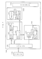
- FIG. 1 is a block diagram showing a configuration of a storage device according to a first embodiment of the present invention.
- a storage device 100 is connected to a host device 110 , writes data after receiving a command (CMD) and data (DATA) from the host device 110 , and reads the data to output the data to the host device 110 .
- the storage device 100 is configured by including a storage medium 120 for retaining data, a host IF unit 130 for executing transmission control with the host device, a control information retaining unit 140 for retaining control information corresponding to the control by the host device 110 , a buffer control unit 150 for temporarily retaining data read and written by the host device 110 , and a control unit 160 .
- the control unit 160 controls the host IF unit 130 , the control information retaining unit 140 , and the buffer control unit 150 .
- the storage medium 120 is a memory for retaining user data, and is composed of, for example, a nonvolatile memory such as a NAND type flash memory.
- the control information retaining unit 140 is configured by including a register 141 and a control information save memory 142 .
- the register 141 is a buffer for retaining, for example, logical address information transmitted form the host device 110 and control information such as a block during being written to the storage medium 120
- the control information save memory 142 is a nonvolatile memory for temporarily saving this information.
- the register 141 may be composed of a nonvolatile RAM.
- the control information save memory 142 is preferably a nonvolatile memory which can be written with higher rate than that of the storage medium 120 , for example, a ferroelectric memory.
- the buffer control unit 150 includes a data buffer 151 , a buffer save memory 152 , and a save flag (F) 153 .
- the data buffer 151 is a volatile memory such as a SRAM. It is enough for a size of the data buffer to be an integral multiplication of a transmission unit of data transmitted from the host device 110 , for example, 512 bytes.
- the buffer save memory 152 is composed of a nonvolatile memory.
- the buffer save memory 152 is preferably a memory which can be written with higher rate than that of the storage medium 120 , for example, a ferroelectric memory.
- a size of the buffer save memory 152 is an integral multiplication of a transmission unit of data transmitted from the host device 110 , be the same size of the data buffer 151 , or be different size.
- the size is preferably equal to or less than that of the buffer memory since the nonvolatile buffer save memory 152 is more expensive and has the smaller number for rewriting than those of the volatile data buffer 151 .
- the save flag 153 is a nonvolatile flag showing existence of saved data when the data is saved into the buffer save memory 152 .
- the save flag 153 may be composed of a nonvolatile memory in integrating with the buffer save memory 152 .
- the control unit 160 includes a system control unit 161 and a save control unit 162 .
- the system control unit 161 controls the host IF unit 130 , the buffer control unit 150 , and the control information retaining unit 140 depending on a transmission request from the host device 110 , and executes data transmission to the storage device 120 .
- the save control unit 162 controls saving and restoring processes for write data and control information, and controls a response to the host.
- FIG. 2A to FIG. 2D , FIG. 3A , and FIG. 3B a writing sequence in the storage device 100 according to the first embodiment will be described below.
- DAT 1 and DAT 2 two units of data, are written will be explained in the present embodiment, however, an applicable scope of the present invention is not limited to the case.
- the host device 110 issues a writing command WCMD to the storage device 100 .
- the command includes a transmission type such as reading or writing, an address of transmitted data, and the like.
- the command is transmitted to the control unit 160 after being received by the host IF unit 130 .
- an address and a type of reading or writing are retrieved from contents of the command as control information shown as “CONT” in the drawing, and are retained in the register 141 of the control information retaining unit 140 .
- FIG. 3A and FIG. 3B are time charts in the case of seeing from the host device.
- the CMD shows a state of a signal line for the host device and the storage device 100 to mutually exchange the control information of a command and a response
- the DATA shows a state of a signal line for the host device and the storage device 100 to transmit write data. Synchronizing with this timing, writing to the data buffer 151 and the storage medium 120 and writing to the save buffer 152 are shown.
- the storage device 100 transmits a command response RES showing reception of the command to the host device.
- the host device transmits write data to the storage device 100 after receiving the command response RES.
- the host IF unit 130 receives the write data DAT 1 .
- the control unit 160 stores the data DAT 1 in the data buffer 151 of the buffer control unit 150 .
- the host device 110 transmits the write data DAT 2 .
- the host IF unit 130 receives the write data DAT 2 .
- the control unit 160 stores the received data DAT 2 in the data buffer 151 of the buffer control unit 150 .
- the write data DAT 1 stored in the data buffer 151 is written into the storage medium 120 .
- the host device 110 issues an end command ECMD to the storage device 100 .
- the host IF unit 130 transmits the command to the control unit 160 .
- the save control unit 162 when receiving the end command, the save control unit 162 generates a save signal, and transmits the save signal to the buffer control unit 150 and the control information storage unit 140 .
- the save signal is generated based on the end command for writing as information regarding writing data obtained from the host device 110 .
- the buffer control unit 150 when receiving the save signal, data during writing stored in the data buffer 151 is saved into the buffer save memory 152 .
- control information (CONT) such as logical addresses and writing blocks stored in the register 141 from the host is saved into the control information save memory 142 .
- the control information (CONT) can be information showing logical address of the data and physical address in which data is to be written (information of writing area address) as data writing.
- the size of the data buffer is enlarged, data whose size is equal to or more than that of the buffer save memory 152 exists in the data buffer 151 . In this case, with saving data into the buffer save memory 152 , data writing is continued to data which is not saved yet, after that, saving can be deemed to be completed at the time when all the writing data in the data buffer 151 are in a safe state.
- FIG. 3A with continuing data writing to the storage medium 120 even after receiving the end command ECMD, data is saved into the buffer save memory 152 .
- a data line may be set to be free by saving data into the buffer save memory 152 .
- data is written from the data buffer 151 to the storage medium 120 . In any of these cases, data is saved into the buffer save memory after receiving the end command ECMD.
- the save flag 153 in the buffer control unit 150 is set.
- the “setting” of the save flag shows existence of data saved in the buffer save memory 152 and the control information save memory 142 .
- the save flag 153 is provided in the buffer control unit 150 in the embodiment of the present invention, however, save flags for respectively showing data saving may be provided in both of the control information retaining unit 140 and the buffer control unit 150 , or the same flag may be provided only in the control information retaining unit 140 . When the save flag is provided to either of them, a necessary resource can be reduced.
- the storage device 100 When receiving the end command ECMD, the storage device 100 is in a busy state by using the DATA line.
- the “busy state” shows that writing data is processed in the storage device 100 , and, in the present embodiment, a case where the DATA line is in low shows that the storage device 100 is in the busy state.
- the writing data DAT 2 and control information are saved into the storage device 100 as explained using FIG. 2D .
- the control unit 160 restores the DATA line to be from in busy state to in normal state, hereby, informs completion of data writing to the host device 110 .
- the host device 110 can recognize the completion of data writing at timing t 1 when the DATA line becomes high.
- time in busy state can be shortened. That is to say, time until completion of data writing, seen from the host device 110 , can be shortened, and processing performance of the storage device can be improved.
- the storage device 100 continues writing of data retained in the data buffer 151 to the storage medium 120 by using saved data or control data retained in the register 141 , and completes the writing processing.
- the save control unit 162 clears the save flag 153 .
- the “clearing” of the save flag 153 shows nonexistence of saved data in the buffer save memory 152 and the control information save memory 142 .
- the power may be shut down by the time of completion of writing because the busy state cannot be found seen from the host device 110 side.
- FIG. 4 is a control flow executed by the control unit 160 in the storage device 100 when the power is supplied to the storage device 100 .
- the control unit 160 executes initialization processing when the power is supplied (S 401 ).
- the control unit 160 checks a bad block in the storage medium 120 and creates a table for converting a logical address issued by the host device into a physical address of the storage medium 120 . While the initialization processing is executed at the power-on in the present embodiment, the processing may be executed when an initialization command is issued from the host device.
- the control unit 160 confirms whether the save flag 153 is set or not (S 402 ). If the flag is set, a size of the saved data is checked (S 403 ). Data reading and writing from the host device 110 is usually performed in a unit called a cluster by using a file system. A size of the cluster is, for example, 16 kB. In a case where a cluster cannot be constituted when the saved data is written into the storage medium 120 again, the data may be meaningless for the host device. For this reason, it is determined whether to process the saved data on the basis of a threshold showing whether one cluster can be constituted in the storage medium 120 by writing saved data to the storage medium 120 , for example.
- the threshold may be specifically determined in the storage device 100 , and may be able to be set by the host device.
- restoring processing of the saved data is executed (S 404 ).
- the restoring processing shows a processing for transferring write data retained in the buffer save memory 152 into the data buffer 151 and a processing for transferring the control information retained in the control information save memory 142 into the register 141 .
- write data in the data buffer 151 is written into the storage medium 120 (S 405 ).
- the save flag is cleared (S 406 ), and the processing is completed.
- the save flag is not set in S 402 , the processing is finished.
- the save flag is cleared (S 406 ), and the processing is completed. Accordingly, the saved data is discarded. Also in a case where data less than a threshold remains at S 405 , the data is discarded. After restoring the saved data to the data buffer 151 once and restoring the control information saved in the control information save memory 142 to the register 141 once, and then writing is performed, however, the restoring processing may be omitted with performing writing to the storage medium 120 directly by using contents of the control information save memory 142 and the buffer save memory 152 .
- a highly reliable storage device can be provided.
- the nonvolatile buffer save memory has the smaller number of rewriting and is highly cost than those of the volatile memory such as a SRAM, a highly reliable storage device can be realized with reducing the number of using the buffer save memory by writing to the buffer save memory only when the host device informs a completion of writing.
- a second embodiment of the present invention will be described. An entire configuration of the present embodiment is the same as the case of FIG. 1 .
- the host device issues a writing command after informing a size of data to be transmitted to the storage device preliminarily.
- the storage device after receiving data of the size preliminarily informed, the storage device retains unwritten data in the data buffer 151 into the buffer save memory 152 and retains control information in the register 141 into the control information save memory 142 , and then the storage device sets the save flag 153 . This can release a busy state immediately after the completion of the save and can set the host device free quickly.
- a save signal is generated based on the size of data informed as information regarding writing data provided from the host device 110 .
- unwritten data retained in the data buffer 151 is written into the storage medium 120 by using control information of the register 141 , subsequently.
- data retained in the buffer save memory 152 is written in the storage medium 120 by using control information retained in the control information save memory 142 after the next power supply.
- FIG. 5 is a block diagram showing a configuration of a storage device according to the present embodiment. Concerning the same part as those of the first embodiment, the present embodiment omits detailed description by appending the same numerals.
- a control unit 160 A includes a voltage detection unit 163 for detecting the power voltage in addition to the aforementioned system control unit 161 and the save control unit 162 .
- the voltage detection unit 163 detects voltage level applied to the storage device 100 , and generates a reset signal and a voltage dropping detection signal.
- Other components are the same as those of the first embodiment described above.
- FIG. 6 is a view for explaining an operation of the voltage detection unit 163 included in the control unit 160 A.
- the reset signal is cancelled when a voltage level reaches a threshold V TL at time t 1 after power supply.
- the reset signal is a low active signal.
- the voltage dropping detection signal is outputted. This voltage dropping detection signal is outputted until time t 3 at when a voltage drops to the threshold voltage V TL where the reset signal turns to be active.
- FIG. 7 shows an operation of a case where the voltage dropping detection signal is outputted from the voltage detection unit 163 .
- the voltage detection unit 163 transmits a voltage detection signal to the save control unit 162 .
- the save control unit 162 When receiving a voltage dropping detection signal during data writing, the save control unit 162 outputs a save signal to the control information retaining unit 140 and the buffer control unit 150 as shown in FIG. 7 , similarly to the processing explained in FIG. 2D .
- the save control unit 162 outputs a save signal when an end command for writing is issued from the host device 110 and also when reaching a preliminarily transmitted size of writing data similar to the first and second embodiment.
- control information retaining unit 140 when receiving the save signal, the control information (CONT) such as the address and the writing block retained in the register 141 are saved into the control information save memory 142 .
- the buffer control unit 150 receives the save signal, the buffer control unit 150 saves the data DAT 2 into the buffer save memory 152 when the data DAT 2 stored in the data buffer 151 is in being written to the storage medium 120 .
- Such processing is executed when the storage device 100 is accidentally removed during data writing in a case where the storage device 100 is removable and when the power supply is shut down by outward shock. In this case, the saved data is processed at the time when the power is supplied to the storage device 100 . The processing is similar to the case shown in FIG. 4 .
- This embodiment is especially suitable for a hot-pluggable storage device, a potable device and a mobile phone in which the power shut down often occurs by the shock.
- the save flag is set when data is saved into the buffer save memory, however, the save flag may be set when the control information is saved into the control information save memory. In addition, the save flag may be set when data is saved into the buffer save memory and the control information is saved into the control information save memory. Furthermore, the buffer save memory and the control information save memory may use the same nonvolatile memory, and a part of the area in the nonvolatile memory may be set for the control information save, and the other parts of the area may be set for the buffer save. In this case, an area for the save memory may be further provided in the nonvolatile memory.
- control information is retained in the control information save memory at the saving, however, the control information can be written into the storage medium by figuring out the control information from the storage medium in writing data, thus no control information save memory is necessary in this case.
- the storage device according to the present invention can be applied for various apparatuses using a storage device such as a memory card.
Abstract
Description
-
- 100 Storage device
- 110 Host device
- 120 Storage medium
- 140 Control information retaining unit
- 141 Register
- 142 Control information save memory
- 150 Buffer control unit
- 151 Data buffer
- 152 Buffer save memory
- 153 Save flag
- 160 Control unit
- 161 System control unit
- 162 Save control unit
- 163 Voltage detection unit
Claims (16)
Applications Claiming Priority (3)
| Application Number | Priority Date | Filing Date | Title |
|---|---|---|---|
| JP2005091930 | 2005-03-28 | ||
| JP2005-091930 | 2005-03-28 | ||
| PCT/JP2006/305964 WO2006104036A1 (en) | 2005-03-28 | 2006-03-24 | Storage device |
Publications (2)
| Publication Number | Publication Date |
|---|---|
| US20090019194A1 US20090019194A1 (en) | 2009-01-15 |
| US7818477B2 true US7818477B2 (en) | 2010-10-19 |
Family
ID=37053293
Family Applications (1)
| Application Number | Title | Priority Date | Filing Date |
|---|---|---|---|
| US11/909,749 Expired - Fee Related US7818477B2 (en) | 2005-03-28 | 2006-03-24 | Storage device with buffer control unit |
Country Status (3)
| Country | Link |
|---|---|
| US (1) | US7818477B2 (en) |
| JP (1) | JP4881856B2 (en) |
| WO (1) | WO2006104036A1 (en) |
Cited By (2)
| Publication number | Priority date | Publication date | Assignee | Title |
|---|---|---|---|---|
| US20180129416A1 (en) * | 2016-11-04 | 2018-05-10 | Samsung Electronics Co., Ltd. | Storage device and data processing system including the same |
| US10649898B2 (en) | 2017-07-03 | 2020-05-12 | Samsung Electronics Co., Ltd. | Memory system, memory controller for memory system, operation method of memory controller, and operation method of user device including memory device |
Families Citing this family (11)
| Publication number | Priority date | Publication date | Assignee | Title |
|---|---|---|---|---|
| JP5014259B2 (en) * | 2008-05-30 | 2012-08-29 | パナソニック株式会社 | Display control apparatus and display control method |
| JP2010086009A (en) * | 2008-09-29 | 2010-04-15 | Hitachi Ltd | Storage device and memory control method |
| JP2010258608A (en) * | 2009-04-22 | 2010-11-11 | Sony Corp | Imaging apparatus and start-up method of imaging apparatus |
| JP5347779B2 (en) | 2009-07-07 | 2013-11-20 | ソニー株式会社 | MEMORY DEVICE, MEMORY CONTROL METHOD, AND PROGRAM |
| JP5366885B2 (en) * | 2010-05-25 | 2013-12-11 | 日立オートモティブシステムズ株式会社 | Electronic control unit |
| CN102799392B (en) * | 2012-06-16 | 2015-12-16 | 北京忆恒创源科技有限公司 | Memory device and interrupt control method thereof |
| US10643668B1 (en) * | 2013-08-27 | 2020-05-05 | Seagate Technology Llc | Power loss data block marking |
| US9858003B2 (en) * | 2016-05-02 | 2018-01-02 | Toshiba Memory Corporation | Storage system that reliably stores lower page data |
| KR102609473B1 (en) * | 2016-06-17 | 2023-12-04 | 에스케이하이닉스 주식회사 | Data storage device and operating method thereof |
| CN109074301B (en) * | 2017-03-13 | 2021-10-08 | 荣耀终端有限公司 | Data processing method and device |
| CN110989918B (en) * | 2018-10-03 | 2023-03-28 | 慧荣科技股份有限公司 | Write control method, data storage device and controller thereof |
Citations (11)
| Publication number | Priority date | Publication date | Assignee | Title |
|---|---|---|---|---|
| JPS6476346A (en) | 1987-09-18 | 1989-03-22 | Fujitsu Ltd | Disk cache control system |
| JPH07200418A (en) | 1993-12-28 | 1995-08-04 | Hitachi Maxell Ltd | Data storage device and its control method |
| US5519831A (en) * | 1991-06-12 | 1996-05-21 | Intel Corporation | Non-volatile disk cache |
| US5596708A (en) * | 1994-04-04 | 1997-01-21 | At&T Global Information Solutions Company | Method and apparatus for the protection of write data in a disk array |
| JPH10154101A (en) | 1996-11-26 | 1998-06-09 | Toshiba Corp | Data storage system and cache controlling method applying to the system |
| US5799200A (en) * | 1995-09-28 | 1998-08-25 | Emc Corporation | Power failure responsive apparatus and method having a shadow dram, a flash ROM, an auxiliary battery, and a controller |
| JPH11143788A (en) | 1997-11-05 | 1999-05-28 | Hitachi Ltd | Outside storage device using non-volatile memory |
| US6289416B1 (en) * | 1997-08-26 | 2001-09-11 | International Business Machines Corporation | Disk drive device and a method for controlling the same |
| US6693840B2 (en) * | 2001-10-17 | 2004-02-17 | Matsushita Electric Industrial Co., Ltd. | Non-volatile semiconductor memory device with enhanced erase/write cycle endurance |
| US6862673B2 (en) * | 2001-11-14 | 2005-03-01 | Silicon Integrated Systems Corporation | Command order maintenance scheme for multi-in/multi-out FIFO in multi-threaded I/O links |
| US7380055B2 (en) * | 2004-06-21 | 2008-05-27 | Dot Hill Systems Corporation | Apparatus and method in a cached raid controller utilizing a solid state backup device for improving data availability time |
-
2006
- 2006-03-24 WO PCT/JP2006/305964 patent/WO2006104036A1/en active Application Filing
- 2006-03-24 JP JP2007510448A patent/JP4881856B2/en not_active Expired - Fee Related
- 2006-03-24 US US11/909,749 patent/US7818477B2/en not_active Expired - Fee Related
Patent Citations (11)
| Publication number | Priority date | Publication date | Assignee | Title |
|---|---|---|---|---|
| JPS6476346A (en) | 1987-09-18 | 1989-03-22 | Fujitsu Ltd | Disk cache control system |
| US5519831A (en) * | 1991-06-12 | 1996-05-21 | Intel Corporation | Non-volatile disk cache |
| JPH07200418A (en) | 1993-12-28 | 1995-08-04 | Hitachi Maxell Ltd | Data storage device and its control method |
| US5596708A (en) * | 1994-04-04 | 1997-01-21 | At&T Global Information Solutions Company | Method and apparatus for the protection of write data in a disk array |
| US5799200A (en) * | 1995-09-28 | 1998-08-25 | Emc Corporation | Power failure responsive apparatus and method having a shadow dram, a flash ROM, an auxiliary battery, and a controller |
| JPH10154101A (en) | 1996-11-26 | 1998-06-09 | Toshiba Corp | Data storage system and cache controlling method applying to the system |
| US6289416B1 (en) * | 1997-08-26 | 2001-09-11 | International Business Machines Corporation | Disk drive device and a method for controlling the same |
| JPH11143788A (en) | 1997-11-05 | 1999-05-28 | Hitachi Ltd | Outside storage device using non-volatile memory |
| US6693840B2 (en) * | 2001-10-17 | 2004-02-17 | Matsushita Electric Industrial Co., Ltd. | Non-volatile semiconductor memory device with enhanced erase/write cycle endurance |
| US6862673B2 (en) * | 2001-11-14 | 2005-03-01 | Silicon Integrated Systems Corporation | Command order maintenance scheme for multi-in/multi-out FIFO in multi-threaded I/O links |
| US7380055B2 (en) * | 2004-06-21 | 2008-05-27 | Dot Hill Systems Corporation | Apparatus and method in a cached raid controller utilizing a solid state backup device for improving data availability time |
Non-Patent Citations (4)
| Title |
|---|
| English language Abstract of JP 10-154101. |
| English language Abstract of JP 11-143788. |
| English language Abstract of JP 64-076346. |
| English language Abstract of JP 7-200418. |
Cited By (3)
| Publication number | Priority date | Publication date | Assignee | Title |
|---|---|---|---|---|
| US20180129416A1 (en) * | 2016-11-04 | 2018-05-10 | Samsung Electronics Co., Ltd. | Storage device and data processing system including the same |
| US10528264B2 (en) * | 2016-11-04 | 2020-01-07 | Samsung Electronics Co., Ltd. | Storage device and data processing system including the same |
| US10649898B2 (en) | 2017-07-03 | 2020-05-12 | Samsung Electronics Co., Ltd. | Memory system, memory controller for memory system, operation method of memory controller, and operation method of user device including memory device |
Also Published As
| Publication number | Publication date |
|---|---|
| JPWO2006104036A1 (en) | 2008-09-04 |
| JP4881856B2 (en) | 2012-02-22 |
| WO2006104036A1 (en) | 2006-10-05 |
| US20090019194A1 (en) | 2009-01-15 |
Similar Documents
| Publication | Publication Date | Title |
|---|---|---|
| US7818477B2 (en) | Storage device with buffer control unit | |
| US8484409B2 (en) | Nonvolatile memory controller with logical defective cluster table | |
| US7624298B2 (en) | Memory card, data processor, memory card control method and memory card setting | |
| US7613871B2 (en) | Storage system using a flash memory partitioned with write-once and rewritable blocks | |
| KR101115843B1 (en) | Semiconductor memory device | |
| WO2009081392A1 (en) | A storage device coordinator and a host device that includes the same | |
| CN101251826A (en) | Flash memory, method and apparatus for data management of flash memory | |
| US20180107432A1 (en) | Storage device and control method | |
| EP0890955A2 (en) | Storage apparatus, data write-in method, and data read-out method | |
| EP3142014A1 (en) | Method, device and user equipment for reading/writing data in nand flash | |
| US20130339584A1 (en) | Method for accessing flash memory having pages used for data backup and associated memory device | |
| US8832407B2 (en) | Communication device with storage function | |
| CN110781029A (en) | Power-off protection method and system | |
| CN109426627B (en) | Data storage device and operation method thereof | |
| US20100005229A1 (en) | Flash memory apparatus and method for securing a flash memory from data damage | |
| JP2007164355A (en) | Non-volatile storage device, data reading method therefor, and data writing method therefor | |
| US20230289059A1 (en) | Memory system and operating method thereof | |
| KR102527925B1 (en) | Memory system and operating method thereof | |
| JP2007087118A (en) | Controller and portable terminal | |
| KR20200043814A (en) | Memory system and operating method thereof | |
| US11249895B2 (en) | Memory controller and memory system | |
| US11513722B2 (en) | Memory system allowing operation during suspensions | |
| JP3017524B2 (en) | Data recording method and IC memory card system in IC memory card | |
| CN108614779A (en) | Data processing method, NANDflash storage devices for NANDflash storage devices | |
| US7330944B2 (en) | Method for storing data in a memory, a system, an electronic device and a memory card |
Legal Events
| Date | Code | Title | Description |
|---|---|---|---|
| AS | Assignment |
Owner name: MATSUSHITA ELECTRIC INDUSTRIAL CO., LTD., JAPAN Free format text: ASSIGNMENT OF ASSIGNORS INTEREST;ASSIGNORS:TOYAMA, MASAYUKI;NAKANISHI, MASAHIRO;IZUMI, TOMOAKI;AND OTHERS;REEL/FRAME:020200/0165 Effective date: 20071107 |
|
| AS | Assignment |
Owner name: PANASONIC CORPORATION, JAPAN Free format text: CHANGE OF NAME;ASSIGNOR:MATSUSHITA ELECTRIC INDUSTRIAL CO., LTD.;REEL/FRAME:021832/0197 Effective date: 20081001 Owner name: PANASONIC CORPORATION,JAPAN Free format text: CHANGE OF NAME;ASSIGNOR:MATSUSHITA ELECTRIC INDUSTRIAL CO., LTD.;REEL/FRAME:021832/0197 Effective date: 20081001 |
|
| STCF | Information on status: patent grant |
Free format text: PATENTED CASE |
|
| FEPP | Fee payment procedure |
Free format text: PAYOR NUMBER ASSIGNED (ORIGINAL EVENT CODE: ASPN); ENTITY STATUS OF PATENT OWNER: LARGE ENTITY |
|
| FPAY | Fee payment |
Year of fee payment: 4 |
|
| MAFP | Maintenance fee payment |
Free format text: PAYMENT OF MAINTENANCE FEE, 8TH YEAR, LARGE ENTITY (ORIGINAL EVENT CODE: M1552) Year of fee payment: 8 |
|
| FEPP | Fee payment procedure |
Free format text: MAINTENANCE FEE REMINDER MAILED (ORIGINAL EVENT CODE: REM.); ENTITY STATUS OF PATENT OWNER: LARGE ENTITY |
|
| LAPS | Lapse for failure to pay maintenance fees |
Free format text: PATENT EXPIRED FOR FAILURE TO PAY MAINTENANCE FEES (ORIGINAL EVENT CODE: EXP.); ENTITY STATUS OF PATENT OWNER: LARGE ENTITY |
|
| STCH | Information on status: patent discontinuation |
Free format text: PATENT EXPIRED DUE TO NONPAYMENT OF MAINTENANCE FEES UNDER 37 CFR 1.362 |
|
| FP | Lapsed due to failure to pay maintenance fee |
Effective date: 20221019 |