US8737136B2 - Apparatus and method for determining a read level of a memory cell based on cycle information - Google Patents
Apparatus and method for determining a read level of a memory cell based on cycle information Download PDFInfo
- Publication number
- US8737136B2 US8737136B2 US13/076,340 US201113076340A US8737136B2 US 8737136 B2 US8737136 B2 US 8737136B2 US 201113076340 A US201113076340 A US 201113076340A US 8737136 B2 US8737136 B2 US 8737136B2
- Authority
- US
- United States
- Prior art keywords
- read
- memory
- controller
- level voltage
- read level
- Prior art date
- Legal status (The legal status is an assumption and is not a legal conclusion. Google has not performed a legal analysis and makes no representation as to the accuracy of the status listed.)
- Active, expires
Links
- 238000000034 method Methods 0.000 title claims abstract description 81
- 230000006870 function Effects 0.000 claims abstract description 54
- 238000003860 storage Methods 0.000 claims description 45
- 230000008569 process Effects 0.000 claims description 40
- 238000012937 correction Methods 0.000 claims description 24
- 238000006073 displacement reaction Methods 0.000 claims description 7
- 238000005516 engineering process Methods 0.000 description 53
- 238000009826 distribution Methods 0.000 description 45
- 238000010586 diagram Methods 0.000 description 15
- 238000013500 data storage Methods 0.000 description 12
- 238000012360 testing method Methods 0.000 description 9
- 238000012512 characterization method Methods 0.000 description 8
- 238000007667 floating Methods 0.000 description 8
- 230000014759 maintenance of location Effects 0.000 description 8
- 238000013461 design Methods 0.000 description 4
- 230000004044 response Effects 0.000 description 4
- 230000001133 acceleration Effects 0.000 description 3
- 239000000872 buffer Substances 0.000 description 3
- 230000015556 catabolic process Effects 0.000 description 3
- 230000008859 change Effects 0.000 description 3
- 238000006731 degradation reaction Methods 0.000 description 3
- 238000012986 modification Methods 0.000 description 3
- 230000004048 modification Effects 0.000 description 3
- 230000009897 systematic effect Effects 0.000 description 3
- 238000012795 verification Methods 0.000 description 3
- 238000004364 calculation method Methods 0.000 description 2
- 230000001351 cycling effect Effects 0.000 description 2
- 230000007423 decrease Effects 0.000 description 2
- 238000002347 injection Methods 0.000 description 2
- 239000007924 injection Substances 0.000 description 2
- 230000007246 mechanism Effects 0.000 description 2
- 239000007787 solid Substances 0.000 description 2
- 230000005641 tunneling Effects 0.000 description 2
- 230000004913 activation Effects 0.000 description 1
- 230000003044 adaptive effect Effects 0.000 description 1
- 238000013459 approach Methods 0.000 description 1
- 238000003491 array Methods 0.000 description 1
- 230000006399 behavior Effects 0.000 description 1
- 230000005540 biological transmission Effects 0.000 description 1
- 230000003139 buffering effect Effects 0.000 description 1
- 238000004891 communication Methods 0.000 description 1
- 239000004020 conductor Substances 0.000 description 1
- 230000008878 coupling Effects 0.000 description 1
- 238000010168 coupling process Methods 0.000 description 1
- 238000005859 coupling reaction Methods 0.000 description 1
- 230000006866 deterioration Effects 0.000 description 1
- 230000002542 deteriorative effect Effects 0.000 description 1
- 230000000694 effects Effects 0.000 description 1
- 239000000835 fiber Substances 0.000 description 1
- 239000002784 hot electron Substances 0.000 description 1
- OCUUDCWEKWOMFA-UHFFFAOYSA-N imidazol-1-yl-dimethyl-propan-2-ylsilane Chemical compound CC(C)[Si](C)(C)N1C=CN=C1 OCUUDCWEKWOMFA-UHFFFAOYSA-N 0.000 description 1
- 238000004519 manufacturing process Methods 0.000 description 1
- 238000013507 mapping Methods 0.000 description 1
- 230000000116 mitigating effect Effects 0.000 description 1
- 230000003287 optical effect Effects 0.000 description 1
- 230000002093 peripheral effect Effects 0.000 description 1
- 230000002035 prolonged effect Effects 0.000 description 1
- 238000013442 quality metrics Methods 0.000 description 1
- 238000011084 recovery Methods 0.000 description 1
- 230000000717 retained effect Effects 0.000 description 1
- 230000035945 sensitivity Effects 0.000 description 1
- 238000013403 standard screening design Methods 0.000 description 1
- 239000000758 substrate Substances 0.000 description 1
- 238000012546 transfer Methods 0.000 description 1
- 230000001960 triggered effect Effects 0.000 description 1
Images


Classifications
-
- G—PHYSICS
- G11—INFORMATION STORAGE
- G11C—STATIC STORES
- G11C16/00—Erasable programmable read-only memories
- G11C16/02—Erasable programmable read-only memories electrically programmable
- G11C16/06—Auxiliary circuits, e.g. for writing into memory
- G11C16/26—Sensing or reading circuits; Data output circuits
-
- G—PHYSICS
- G11—INFORMATION STORAGE
- G11C—STATIC STORES
- G11C16/00—Erasable programmable read-only memories
- G11C16/02—Erasable programmable read-only memories electrically programmable
- G11C16/06—Auxiliary circuits, e.g. for writing into memory
- G11C16/10—Programming or data input circuits
-
- G—PHYSICS
- G11—INFORMATION STORAGE
- G11C—STATIC STORES
- G11C11/00—Digital stores characterised by the use of particular electric or magnetic storage elements; Storage elements therefor
- G11C11/56—Digital stores characterised by the use of particular electric or magnetic storage elements; Storage elements therefor using storage elements with more than two stable states represented by steps, e.g. of voltage, current, phase, frequency
- G11C11/5621—Digital stores characterised by the use of particular electric or magnetic storage elements; Storage elements therefor using storage elements with more than two stable states represented by steps, e.g. of voltage, current, phase, frequency using charge storage in a floating gate
- G11C11/5628—Programming or writing circuits; Data input circuits
-
- G—PHYSICS
- G11—INFORMATION STORAGE
- G11C—STATIC STORES
- G11C11/00—Digital stores characterised by the use of particular electric or magnetic storage elements; Storage elements therefor
- G11C11/56—Digital stores characterised by the use of particular electric or magnetic storage elements; Storage elements therefor using storage elements with more than two stable states represented by steps, e.g. of voltage, current, phase, frequency
- G11C11/5621—Digital stores characterised by the use of particular electric or magnetic storage elements; Storage elements therefor using storage elements with more than two stable states represented by steps, e.g. of voltage, current, phase, frequency using charge storage in a floating gate
- G11C11/5642—Sensing or reading circuits; Data output circuits
Definitions
- the subject technology relates generally to memory devices and in particular multi-level cell flash memory devices.
- Flash memory bears little resemblance to a magnetic recording system.
- Commodity flash chips are closed systems with no external access to analog signals, in sharp contrast to the typical Hard Disk Drive (HDD) where analog signals have always been available for study.
- HDD Hard Disk Drive
- the performance of flash memory is known to degrade through the life cycle and has a finite life. Consequently, since flash memory was first conceived as a memory device the target error rate at the output of the chip has been very low, as opposed to systems where stronger Error Correction Coding (ECC) may be used.
- ECC Error Correction Coding
- SSD Solid State Drives
- MLC multi-level cell
- SLC single-level cell
- Consumer SSD manufacturers have mitigated such problems by employing interleaving and/or providing excess capacity in conjunction with wear-leveling algorithms.
- MLC flash endurance has not been proven acceptable for enterprise SSD applications. Even with the increased data capacity of MLC, it becomes more expensive in enterprise applications because of its disproportionately large decrease in program/erase (P/E) cycles over time due to increased (wear causing) stresses required to read, program and erase the flash, causing a gradual degradation in endurance.
- P/E program/erase
- a method for determining a read level voltage to apply to a memory cell in a flash memory circuit includes comparing a prediction value to a prediction indicator to determine whether a previous RL voltage should be used or a new RL voltage should be estimated, calculating the RL voltage as a function of the a first RL voltage and an estimation parameter when the RL voltage should be estimated, and providing to the memory circuit a programming command representative of the RL voltage to read the memory cell.
- the method determines the RL voltage should be estimated when the read operation is a first read after a write operation or a read address is equal to a marginal address or a read level margin (RLM) value reaches a RLM threshold value, the RLM value being calculated when the read operation is the first read after the write operation and the read address is equal to the marginal address, the RLM value being calculated as a function of an error level value and a number of program/erase (P/E) cycles.
- RLM read level margin
- the method includes generating at run-time a prediction value, reading a prediction indicator from a lookup table, comparing the prediction value to the prediction indicator to determine whether a RL voltage should be estimated, and, when the RL voltage should be estimated, calculating a temperature factor as a function of a die temperature associated with the memory circuit, calculating a process corner factor as a function of a nominal process corner associated with the memory circuit and a number of P/E cycles, calculating a location correction factor as a function of a block location associated with the memory circuit and a page location associated with the memory circuit, calculating a correction element, calculating an estimation parameter as a function of a memory dwell time, the number of P/E cycles, the temperature factor, the process corner factor, the location correction factor, and the correction element, calculating the RL voltage as a function of the a first RL voltage and the estimation parameter, and providing to the memory circuit a programming command representative of the RL voltage to read the memory cell.
- control circuit for determining a read level (RL) voltage to apply to a memory cell in a non-volatile memory circuit.
- the control circuit includes a memory interface configured to be operably coupled to the memory circuit and a controller, wherein the controller is configured to, on receiving a signal from a host interface representative of a memory read operation associated with the memory circuit, compare a prediction value to a prediction indicator to determine whether the RL voltage should be estimated, calculate the RL voltage as a function of the a first RL voltage and an estimation parameter when the RL voltage should be estimated, and provide to the memory circuit a programming command representative of the RL voltage to read the memory cell.
- the system includes a host interface operably coupled to a host device, to receive data from the host device, and to send data to the host device, a storage medium interface operably coupled to a volatile memory, a memory interface operably coupled to the memory circuit, and a controller, wherein the controller is operable to, on receiving a signal from a host interface representative of a memory read operation associated with the memory circuit, compare a prediction value to a prediction indicator to determine whether the RL voltage should be estimated, calculate the RL voltage as a function of the a first RL voltage and an estimation parameter when the RL voltage should be estimated, and provide to the memory circuit a programming command representative of the RL voltage to read the memory cell.
- a host interface operably coupled to a host device, to receive data from the host device, and to send data to the host device
- a storage medium interface operably coupled to a volatile memory
- a memory interface operably coupled to the memory circuit
- the controller is operable to, on receiving a signal from a host interface representative of a memory read operation
- FIG. 1 is a block diagram illustrating components of a data storage system according to one aspect of the subject technology.
- FIG. 2 is a diagram illustrating an exemplary graph diagram of four possible cell V T distributions and complimentary program verify levels for a group of memory cells in a multi-level cell flash memory according to one aspect of the subject technology.
- FIG. 3 is a graph diagram illustrating an exemplary threshold voltage evolution of a 2-bit MLC NAND flash memory cell with read levels chosen apriori at beginning of life according to one aspect of the subject technology.
- FIG. 4 is a flowchart illustrating a process for predicting when current read levels and/or settings are suspect according to one aspect of the subject technology.
- FIG. 5 is a flowchart illustrating an alternative process for predicting when current read levels and/or settings are suspect according to one aspect of the subject technology.
- FIG. 6 is a flowchart illustrating a process for estimating a Read Level (RL) voltage to apply to the memory cells of a memory block according to one aspect of the subject technology.
- RL Read Level
- FIG. 7 is an exemplary characterization of a 41 nm MLC flash memory depicting a V T shift (mV) at predetermined intervals to achieve a minimum BER over the life of the memory according to one aspect of the subject technology.
- V T shift mV
- FIG. 8A is a graph diagram illustrating die temperature increase relative to drive temperature increase over predetermined intervals of P/E cycles according to one aspect of the subject technology.
- FIG. 8B is a graph diagram illustrating read level offsets for exemplary word lines and their respective pages in a memory block according to one aspect of the subject technology.
- FIG. 9 is a flowchart illustrating an overall process for predicting, estimating and adjusting a read level according to one aspect of the subject technology.
- FIG. 10 is a graph diagram of a voltage threshold adjustment over time and read and write operations according to one aspect of the subject technology.
- memory cells are grouped in strings, with each string consisting of a set of transistors connected in series between a drain select transistor, connected to a bit line of the memory block, and a source select transistor, connected to a reference voltage distribution line.
- Each memory cell includes a floating-gate MOS transistor.
- F-N Fowler-Nordheim Tunneling and/or hot-electron injection.
- the non-volatility of the cell is due to the electrons maintained within the floating-gate.
- Bits are stored by trapping charge on the floating gate (an electrically isolated conductor) which stores a logic value defined by its threshold voltage (read threshold) commensurate with the electric charge stored.
- the electrons in the floating gate are pulled off by quantum tunneling (a tunnel current) from the floating gate to, for example, the source and/or substrate.
- a flash memory As a flash memory is cycled (that is, programmed and erased repeatedly), its physical qualities change. For example, the repeated placement and removal of electrons on the floating gate during programming and erase operations, respectively, causes some excess electrons to be trapped in the device. Also, when one or multiple cells are programmed, adjacent cells may experience an unexpected and undesired charge injection to their floating gates, thus leading to corruption of data stored therein. For instance, electrons may leak into neighboring cells after prolonged stress due to the voltages at the gates of neighboring cells. The threshold voltages of these memory cells may eventually take values that are different (higher or lower) than expected values, causing errors when the data is read.
- the damage done becomes a function of the field strength (voltage) and duration; that is, programming the flash memory to high threshold voltage conditions increases the rate of damage arising from both program and erase processes because it requires longer duration and/or higher applied fields. For instance, adding enough electrons can change a cell from an erased state to a programmed state.
- FIG. 1 is a block diagram illustrating components of a data storage system according to one aspect of the subject technology.
- data storage system 100 (for example, a solid state drive) includes data storage controller 101 , storage medium 102 , and flash memory 103 .
- Controller 101 may use storage medium 102 for temporary storage of data and information used to manage data storage system 100 .
- Controller 101 may include several internal components (not shown) such as a read-only memory, a flash component interface (for example, a multiplexer to manage instruction and data transport along a serial connection to flash memory 103 ), an I/O interface, error correction circuitry, and the like.
- all of these elements of controller 101 may be integrated into a single chip. In other aspects, these elements may be separated on their own PC board.
- Controller 101 may also include a processor that may be configured to execute code or instructions to perform the operations and functionality described herein, manage request flow and address mappings, and to perform calculations and generate commands.
- the processor of controller 101 may be configured to monitor and/or control the operation of the components in data storage controller 101 .
- the processor may be a general-purpose microprocessor, a microcontroller, a digital signal processor (DSP), an application specific integrated circuit (ASIC), a field programmable gate array (FPGA), a programmable logic device (PLD), a controller, a state machine, gated logic, discrete hardware components, or a combination of the foregoing.
- DSP digital signal processor
- ASIC application specific integrated circuit
- FPGA field programmable gate array
- PLD programmable logic device
- controller a state machine, gated logic, discrete hardware components, or a combination of the foregoing.
- One or more sequences of instructions may be stored as firmware on ROM within controller 101 and/or its processor.
- One or more sequences of instructions may be software stored and read from storage medium 102 , flash memory 103 , or received from host device 104 (for example, via host interface 105 ).
- ROM, storage medium 102 , flash memory 103 represent examples of machine or computer readable media on which instructions/code executable by controller 101 and/or its processor may be stored.
- Machine or computer readable media may generally refer to any medium or media used to provide instructions to controller 101 and/or its processor, including volatile media, such as dynamic memory used for storage media 102 or for buffers within controller 101 , and non-volatile media, such as electronic media, optical media, and magnetic media.
- controller 101 may be configured to store data received from a host device 104 in flash memory 103 in response to a write command from host device 104 . Controller 101 is further configured to read data stored in flash memory 103 and to transfer the read data to host device 104 in response to a read command from host device 104 . As will be described in more detail below, controller 101 is also configured to predict when current read levels and/or settings are suspect and to estimate new read levels when it is predicted that the current read levels and/or settings need to be changed. If the estimated read levels are proven to be insufficient, controller 101 may be configured to perform further iterative adjustments to correct the read level parameters.
- the subject technology may extend the number of P/E operations that may be performed on memory cells within flash memory 103 in a particular application environment, and increase the endurance of the memory cells compared to the same application environment operating without the ability to dynamically adjust read levels.
- Host device 104 represents any device configured to be coupled to data storage system 100 and to store data in data storage system 100 .
- Host device 104 may be a computing system such as a personal computer, a server, a workstation, a laptop computer, PDA, smart phone, and the like.
- host device 104 may be an electronic device such as a digital camera, a digital audio player, a digital video recorder, and the like.
- storage medium 102 represents volatile memory used to temporarily store data and information used to manage data storage system 100 .
- storage medium 102 is random access memory (RAM) such as double data rate (DDR) RAM.
- RAM random access memory
- DDR double data rate
- Other types of RAM also may be used to implement storage medium 102 .
- Memory 102 may be implemented using a single RAM module or multiple RAM modules. While storage medium 102 is depicted as being distinct from controller 101 , those skilled in the art will recognize that storage medium 102 may be incorporated into controller 101 without departing from the scope of the subject technology.
- storage medium 102 may be a non-volatile memory such as a magnetic disk, flash memory, peripheral SSD, and the like.
- data storage system 100 may also include host interface 105 .
- Host interface 105 may be configured to be operably coupled (for example, by wired or wireless connection) to host device 104 , to receive data from host device 104 and to send data to host device 104 .
- Host interface 105 may include electrical and physical connections, or a wireless connection, for operably coupling host device 104 to controller 101 (for example, via the I/O interface of controller 101 ).
- Host interface 105 may be configured to communicate data, addresses, and control signals between host device 104 and controller 101 .
- the I/O interface of controller 101 may include and/or be combined with host interface 105 .
- Host interface 105 may be configured to implement a standard interface, such as Serial-Attached SCSI (SAS), Fiber Channel interface, PCI Express (PCIe), SATA, USB, and the like. Host interface 105 may be configured to implement only one interface. Alternatively, host interface 105 (and/or the I/O interface of controller 101 ) may be configured to implement multiple interfaces, which may be individually selectable using a configuration parameter selected by a user or programmed at the time of assembly. Host interface 105 may include one or more buffers for buffering transmissions between host device 104 and controller 101 .
- SAS Serial-Attached SCSI
- PCIe PCI Express
- SATA Serial-Attached SCSI
- USB Universal Serial-Attached SCSI
- Host interface 105 may be configured to implement only one interface. Alternatively, host interface 105 (and/or the I/O interface of controller 101 ) may be configured to implement multiple interfaces, which may be individually selectable using a configuration parameter
- Flash memory 103 represents a non-volatile memory device for storing data.
- flash memory 103 includes, for example, a NAND flash memory.
- Flash memory 103 may include a single flash memory device or chip, or, as depicted by FIG. 1 , may include multiple flash memory devices or chips arranged in multiple channels. Flash memory 103 is not limited to any particular capacity or configuration. For example, the number of physical blocks, the number of physical pages per physical block, the number of sectors per physical page, and the size of the sectors may vary within the scope of the subject technology.
- Flash memory may have a standard interface specification. This standard ensures that chips from multiple manufacturers can be used interchangeably (at least to a large degree).
- the interface hides the inner working of the flash and returns only internally detected bit values for data.
- the interface of flash memory 103 is used to access one or more internal registers 106 and an internal flash controller 107 for communication by external devices.
- registers 106 may include address, command, and/or data registers, which internally retrieve and output the necessary data to and from a NAND memory cell array 108 .
- a data register may include data to be stored in memory array 108 , or data after a fetch from memory array 108 , and may also be used for temporary data storage and/or act like a buffer.
- An address register may store the memory address from which data will be fetched to host 104 or the address to which data will be sent and stored.
- a command register is included to control parity, interrupt control, and the like.
- internal flash controller 107 is accessible via a control register to control the general behavior of flash memory 103 .
- Internal flash controller 107 and/or the control register may control the number of stop bits, word length, receiver clock source, and may also control switching the addressing mode, paging control, coprocessor control, and the like.
- registers 106 may also include a test register.
- the test register may be accessed by specific addresses and/or data combinations provided at the interface of flash memory 103 (for example, by specialized software provided by the manufacturer to perform various tests on the internal components of the flash memory).
- the test register may be used to access and/or modify other internal registers, for example the command and/or control registers.
- test modes accessible via the test register may be used to input or modify certain programming conditions of flash memory 103 (for example, read levels) to dynamically vary how data is read from the memory cells of memory arrays 108 .
- FIG. 2 is a diagram illustrating an exemplary graph diagram of four possible cell V T distributions and complimentary program verify levels for a group of memory cells in a multi-level cell flash memory according to one aspect of the subject technology.
- a MLC NAND cell is capable of storing four states (levels of charge) per cell, yielding two logical bits of information per cell: the Most Significant Bit (MSB) and Least Significant Bit (LSB). These two bits may make up corresponding MSB and LSB pages of a memory block.
- MSB Most Significant Bit
- LSB Least Significant Bit
- a NAND memory block is programmed one page at a time using an Incremental Step Programming Procedure (ISSP) and erased using a similar Incremental Step Erase Procedure (ISEP).
- the ISPP and/or ISEP may be performed by flash controller 107 in response to one or more commands received from controller 101 .
- the memory cells that are to be programmed may be selected at the bit line.
- a “page operation” may be performed to apply a voltage at the gates of each cell in the memory page.
- a corresponding selection at the bit lines creates a voltage potential in the selected group of memory cells where the LSB is selected to be different (for example, binary 10 or 00) than the erased L0 distribution state 201 (for example, binary 11).
- ISPP increases 202 the threshold voltage V T 203 in the floating gates of the selected group of cells to create LSB distribution 204 .
- ISPP is applied to create an L1 distribution 205 from the erased L0 distribution 201 (for example, binary 01), or, an L2 distribution 206 (for example, binary 00) or L3 distribution 207 (for example, binary 10) from the previously programmed LSB distribution 204 .
- L0 distribution 201 for example, binary 01
- L2 distribution 206 for example, binary 00
- L3 distribution 207 for example, binary 10
- the ISPP includes a series of voltage pulses that are applied in a step pattern with the amplitude of each pulse incrementally increased with increasing pulse number, starting from a certain starting magnitude.
- flash controller 107 of flash memory 103 may perform a programming verification (sensing) operation in between each step. Alternatively, this verification operation may be performed after a specific number of steps (the number of steps, for example, being stored on storage medium 102 ). To verify a cell has been successfully programmed, controller 107 applies a program verify voltage 208 in an attempt to conduct the cell. In some aspects, if the threshold voltage of a cell in the memory page is detected above a certain program verify level, flash controller 107 may stop further programming of that single cell by setting it to a program inhibit state.
- LSB and MSB programming use different values of ISPP starting magnitude and/or ISPP step magnitude. Accordingly, a different ISPP step and/or starting magnitudes can be used during the MSB programming of L1 distribution 205 than in the programming of L2 distribution 206 and/or L3 distribution 207 . This is because programming to a higher V T level requires the application of a higher programming voltage potential. It has been found that higher programming pulse magnitudes result in faster programming, and smaller ISPP step magnitudes and/or narrower pulse widths result in narrower final V T distributions (for example, a distribution of cells programmed to the same V T having a smaller standard deviation).
- these parameter values may be stored in storage medium 102 and accessed by controller 101 to determine (for example, calculate) further values and/or issue commands to flash memory 103 .
- Controller 101 may be configured to communicate with flash memory 103 via registers 106 (for example, the test register) and/or flash controller 107 to provide commands for modifying certain parameters (for example, nominal parameters set by the chip manufacturer) of flash memory 103 to vary the V T distributions at run-time and/or to vary the voltages applied to conduct the memory cells (read levels).
- these parameters can be dynamically determined and/or adjusted at run-time as a function of various circuit characteristics (for example, P/E cycle, retention time, BER, temperature) and/or in response to commands received from host 104 via host interface 105 .
- circuit characteristics for example, P/E cycle, retention time, BER, temperature
- FIG. 3 is a graph diagram illustrating an exemplary threshold voltage evolution of a 2-bit MLC NAND flash memory cell with read levels and program verify levels chosen apriori at beginning of life according to one aspect of the subject technology.
- the topmost row represents the four possible distributions of each programming state in a group of memory cells at a memory cell's beginning of life (BOL).
- the respective programming distributions of L0 distribution 201 , L1 distribution 205 , L2 distribution 206 , and L3 distribution 207 are shown along a voltage threshold continuum 301 .
- the middle row of FIG. 3 depicts an exemplary progression of the programming distributions after repeated P/E cycling.
- the buildup of electrons trapped on the floating gates of the memory cells has caused some cells to be programmed with higher voltage thresholds (increasing the standard deviation of the distribution at a higher V T ).
- This shift 306 in voltage thresholds may eventually cause the right edges of the V T distributions to reach the higher adjacent read levels.
- the V T of some of the cells in the distributions begin to cross 307 the higher read levels, the likelihood that a read operation will produce an error increases.
- the bottom row depicts an exemplary result of an extended retention time (for example, dwell time) on the memory cells. After a number of P/E cycles, some of the memory cells that have not been cycled have lost electrons, causing their voltage thresholds to drop (increasing the standard deviation of the deviation at lower V T ).
- This shift 308 may eventually cause the left edges of the V T distributions to reach the lower adjacent read levels. The more cycles over which data is retained the more extreme the decline. If the read levels remain fixed, the V T distributions that have crossed 309 the next lower read level may cause significant errors.
- the edges of each of the distributions are suitably spaced from adjacent read levels.
- spacing can be altered by setting program verify voltages 305 (for example, PV 1 , PV 2 , and/or PV 3 ) during the verification operation sufficiently higher than a lower read level, but sufficiently low enough to prevent even those cells in the distribution having the highest V T (largest deviation) from crossing the next higher read level.
- program verify voltages 305 for example, PV 1 , PV 2 , and/or PV 3
- RL1 voltage 302 will cause cells in L0 distribution 201 to conduct
- RL2 voltage 303 will cause cells in L1 distribution 205 to conduct
- RL3 voltage 304 will cause cells in L2 distribution to conduct, and so on.
- RL voltage 304 will not cause any cells in L3 distribution 207 to conduct, thereby generating a binary x0 in the LSB (see FIG. 2 ) for those cells.
- N distributions there will be N ⁇ 1 read levels. In the depicted example, there are four distributions (of states) and three read levels. Those skilled in the art will recognize that there may be eight, sixteen, or more distributions without departing from the scope of the subject technology.
- Controller 101 may be configured to perform certain prediction operations before reading memory 103 to predict whether the last read level voltage used to read data remains at an acceptable value or whether a new read level voltage should be estimated to compensate for a shift in V T distribution, to reduce BER. In some aspects, these operations may be performed on one or more blocks of memory at a time, however, one skilled in the art will recognize that controller 101 can be manufactured or programmed to perform the operations with regard to any number of cells, including individual cells or one or more pages or strings. In some aspects, controller 101 may be configured to provide the read level prediction in conjunction with estimating a new read level.
- predicting whether a read level should be estimated prior to performing a read operation saves time and power consumption that would otherwise be needed by read level estimations that would occur had the prediction not been performed. Additionally, the cost (time and power) of predicting a read level is specifically less than estimating a read level on every read, and, the chance of success rate has been found to be high, avoiding the cost of a read failure that could otherwise result from not predicting, or mis-predicting, a read level.
- Prediction Success Rate Target >1 ⁇ (Prediction Savings/Cost of Misprediction) (1)
- Prediction Savings Cost of Estimation*(1 ⁇ Frequency of Estimation) ⁇ Cost of Prediction
- Algorithm computation unit power is 0.1 mW/DMIPS
- Prediction algorithms is 100 instructions or clocks per flash read operation
- Estimation algorithm is 1000 instructions or clocks per flash read operation
- Prediction Success Rate will have to be equal to greater than 99% ⁇ 1 ⁇ [1 mW*(1 ⁇ 5%) ⁇ 0.1 mW]/100 mW ⁇ .
- FIG. 4 is a flowchart illustrating a process for predicting when current read levels and/or settings are suspect according to one aspect of the subject technology.
- controller 101 receives from host device 104 an instruction representative of a read operation.
- Controller 101 generates a prediction value, and, in some aspects, determines the prediction value from characteristics associated with the memory block being read. For example, as will be described in more detail below, these characteristics may include whether the last operation on the block was a write operation, whether the page being read is a marginal or critical address, comparing read level margins and read level margin thresholds, and/or a previous read level value (see FIG. 5 ).
- controller 101 may be configured to retrieve the prediction value and/or characteristics from a lookup table stored on storage medium 102 or storage medium 103 , or the like. Controller 101 further retrieves a prediction indicator from a lookup table stored on storage medium 102 .
- the prediction indicator may include a Boolean value, a marginal or critical address, read level margin thresholds, a previous read level value, and/or the like. It is not necessary that the prediction value and predication indicator are generated in any particular sequence but, rather, in some aspects, they may be generated in substantially parallel operations.
- step S 401 controller 101 performs a compare operation to compare the prediction value to the prediction indicator to determine whether a read level voltage should be estimated. If the result of the compare operation is positive (for example, the prediction value and prediction indicator are equal) then the process proceeds to step S 402 to estimate/determine a new read level. Otherwise, the process terminates and a read is performed on the memory using existing read levels and/or parameters.
- Step S 403 controller 101 generates a programming command representative of the new read level voltage to read the memory cell and provides it to flash memory 103 (for example, via registers 106 ).
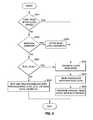
- FIG. 5 is a flowchart illustrating an alternative process for predicting when current read levels and/or settings are suspect according to one aspect of the subject technology.
- controller 101 receives an instruction from host device 104 representative of a read operation.
- step S 501 when reading a block of flash memory 103 , controller 101 determines whether the block is being read for the first time after a write operation. In some aspects, prior to this determination, controller 101 sets a Boolean flag associated with the block to TRUE after a write operation (Just Written Flag). Before a read operation is undertaken, controller 101 determines whether the Boolean flag is TRUE, and if so, sets the flag to FALSE and proceeds to step S 502 to estimate a new read level. In step S 503 , the page and/or block is read using the new read level.
- step S 504 controller 101 determines whether the read address is equal to a marginal address stored on a lookup table in storage medium 102 (for example, by XOR with an address mask).
- a marginal address may be an address that likely needs a specific read level voltage to avoid generating a high BER.
- Those skilled in the art will recognize techniques and methods for determining which addresses are likely to generate a high BER (for example, from a sector bit error memory map). If the read address is equal to the marginal address the process proceeds to step S 502 to estimate a new read level.
- the read level Prior to estimating the new read level, since the new read level was triggered by an address within the block (for example, the first and last pages of the block), the read level may be temporarily modified so that further read levels for the block remain unchanged.
- step S 505 (designated as by dotted lines)
- the present read level is temporarily stored in memory (for example, storage medium 102 , flash memory 103 , or the like), and then the read level estimated in step S 502 and the read performed in step S 503 .
- controller 101 may program the original read level back into memory. In other aspects, if controller 101 determines that the read address is not equal to a marginal address then the process proceeds to step S 507 .
- controller 101 determines a Read Level Margin (RLM) value as a function of an error level value from a previous read, and a number of program/erase (P/E) cycles.
- RLMs reduce as read error levels increase and P/E cycles increase.
- controller 101 determines the error level value as a function of a quality of a previous read operation.
- RLM K EL ⁇ K PE .
- the values associated with K EL and K PE may be indexed by their respective ranges and stored in one or more look up tables (for example, on storage medium 102 ). Controller 101 may access the one or more look up tables to compare the number of error bits generated from the previous read operation to the Error Level ranges to generate K EL , and compares the current number of P/E cycles to the P/E ranges to generate K PE .
- controller 101 determine whether the calculated RLM is greater or equal to a Read Level Margin threshold (RLM T ). If it is then the process proceeds to step S 502 to estimate a new read level. Otherwise, if RLM is less than RLM T , the process proceeds to step S 508 and the previous read level is used.
- Table 1 is an exemplary lookup table of RLM thresholds:
- Table 1 is an exemplary lookup table stored on storage medium 102 which stores RLM values corresponding to EL range limits EL 1 , EL 2 , and EL 3 , and P/E cycle range limits PE 1 , PE 2 , and PE 3 .
- RLM T is set at 16.
- controller 101 determines RLM to be greater than 16 then it will predict that a new read level should be estimated, otherwise, controller 101 will proceed with a read operation using the previous read level.
- a RLM T value is stored for each block.
- one or more RLM T values may be stored for a group of blocks or all blocks.
- storage medium 102 will be sufficient to save the number of error bits generated from the previous read operation and the previous Block Read Level Value (BRLEV) for each block. If controller 101 changes a BRLEV at the completion of a read, controller 101 stores the BRLEV for use by a future read operation for the same block.
- BRLEV Block Read Level Value
- FIG. 6 is a flowchart illustrating a process for estimating a read level voltage to apply to the memory cells of a memory block according to one aspect of the subject technology.
- controller determines that a new read level voltage should be estimated (see FIGS. 4 and 5 ).
- a Voltage Shift due to Dwell Time ( ⁇ V DT ) is determined (for example, calculated) and stored in storage medium 102 for the block being read.
- ⁇ V DT is the optimal V T shift needed to correct a distribution of cells at nominal process conditions and nominal case temperature for different P/E cycles and dwell times.
- ⁇ V DT values may be a result of a flash memory characterization and stored in a lookup table on storage medium 102 .
- the number of columns and rows of the lookup table depends on the number of P/E cycle and dwell time ranges to be covered, and ⁇ V DT precision.
- Storage medium 102 may also include other information relative to ⁇ V DT that is updated periodically, for example, setting and/or storing a Block Time Stamp (representative of the Dwell Time) for each block on each read operation performed on the memory block.
- FIG. 7 an exemplary characterization of a 41 nm MLC flash memory is shown depicting a V T shift (mV) at predetermined intervals to achieve a minimum BER over the life of the memory (for example, a number of P/E cycles) according to one aspect of the subject technology. From this exemplary characterization seven dwell time ranges with quadratic values can be identified. Table 2 is an exemplary lookup table with dwell time ranges defined from 1 ⁇ to 128 ⁇ cross-referenced with eight P/E cycle intervals.
- 1 ⁇ Dwell Time corresponds to 1 ⁇ 2 hour at a Reference Temperature 75 C.
- a 2 hour dwell time will produce a ⁇ 100 mV shift. This allows for covering up to 64 hours, or 2.6 days, time, for which the V T distribution shift is minimal at even a high number of P/E cycles.
- the probability of data lifetimes exceeding 2.5 days has been found to be relatively low, and for which additional read failure recovery mechanisms may be acceptable (for example, ECC).
- ECC additional read failure recovery mechanisms
- dwell times are first converted to the dwell time scale of Table 2 based on the temperature of data storage system 100 (for example, actual drive temperature).
- Storage system 100 includes an internal temperature sensor 109 (for example, a thermocouple or thermometer) that provides system 100 with a drive operating temperature (T S ) measured at a reference location.
- T S drive operating temperature
- T S actual drive operating temperature (K).
- Ea activation energy for the respective failure mechanism: 1.1 eV for NAND flash technology.
- the block's dwell time is multiplied by ⁇ F T prior to referencing the lookup table represented by Table 2 to more accurately predict ⁇ V DT as a function of drive temperature.
- storage system 100 may store a lookup table on storage medium 102 that includes AF T values.
- dwell times are converted to the dwell time scale based on the temperature of flash memory 103 (for example, actual die temperature).
- a drive level temperature characterization may require a die temperature variation against the reference location where temperature sensor 109 is located. It has been found that the temperature variation of flash memory 103 may be somewhat independent from the drive temperature provided by internal temperature sensor 109 . Therefore, in some aspects, the calculation of ⁇ V DT may also include a Die Temperature Adjustment factor (k TF ) to model Temperature Conversion Factor AF T as a factor of die temperature.
- k TF Die Temperature Adjustment factor
- FIG. 8A is a graph diagram illustrating die temperature increase relative to drive temperature increase over predetermined intervals of P/E cycles according to one aspect of the subject technology.
- k TF is generated for the increase in die temperature (for example, at memory 103 ) relative to the drive temperature taken at temperature sensor 109 .
- the data represented in FIG. 8 is stored in one or more lookup tables on storage medium 102 .
- Table 4 provides an exemplary list of Die Temperature Adjustment factors k TF and their percentage change over 75 C for NAND flash memory at a given drive temperature.
- Table 4 can be implemented as a lookup table for k TF , indexed by drive temperature value and/or range.
- the lookup table may be stored on storage medium 102 for access by controller 101 when determining ⁇ V DT . It has been found that, given the base reference value of 75 C, the error of AF T determined from Table 4 is within 15% for the range 40 C to 105 C for NAND flash
- controller 101 determines a process corner factor as a function of a nominal process corner associated with flash memory 103 and a number of P/E cycles.
- Process corners represent the extremes of parameter variations within which a flash memory circuit must function correctly.
- Process variations during the manufacture of the flash memory device may result in different electrical parameters which may affect device characteristics, including data retention.
- a process variation may cause a ⁇ V DT shift acceleration over time and temperature.
- a ⁇ V DT Shift Acceleration Factor (k PC ) may be defined at different P/E cycles for different process corner values and stored on storage medium 102 .
- Table 5 is an exemplary lookup table for determining a process corner factor (k PC ) as a scaling factor to be used when estimating the new RL voltage.
- Column S Slow Corner ( ⁇ 1 s);
- Column T Typical Corner (0 s);
- Column F Fast Corner (+1 s); and
- Column FF Very Fast Corner (+3 s).
- controller 101 determines Location Correction Factors as a function of a Block Location/Address in memory cell array 108 and/or a Page Location/Address in the block.
- block location and page address result in different variations of V T shift over P/E cycles.
- flash characterization can provide further address dependency and sensitivity (scaling) factors.
- Block locations and/or page locations sensitive to V T shift are stored in one or more lookup tables on storage medium 102 , and indexed by P/E cycle or range of P/E cycles. Each block location is associated with a Block Address Factor k BK , and each Page Location is associated with a Page Address Factor k PG .
- a logical mask to a flash memory address may be used to identify a page address and/or a block address range(s) to determine what scaling factors to use.
- Controller 101 may access the one or more lookup tables on storage medium 102 to retrieve factors k BK and k PG and apply those values as factors in estimating the new read level voltage.
- controller 101 determines a Systematic Correction Factor S CF .
- controller 101 collects information related to a read operation (for example, BER, V T used, and the like) to verify the quality of the read operation. If the quality is below a predetermined level (for example, determined by ECC), controller may determine S CF from BER, statistics on errors from previous read operations, V T displacement from re-read iterations following a read failure, and the like.
- S CF may be known apriori.
- S CF may be determined during a flash read level characterization before product implementation, and/or computed by a procedure executed by controller 101 (or other processor and/or circuit) through post-process read error and read retry operations.
- controller 101 or other processor and/or circuit
- S CF is added to the read level estimation (for example, as a read level offset).
- FIG. 8B is a graph diagram illustrating read level offsets for exemplary word lines and their respective pages in a memory block according to one aspect of the subject technology.
- pages associated with word line 0 may have a S CF of 200 mV versus pages associated with world line 32 (WL32)
- pages in word line 63 may have a S CF of ⁇ 300 mV versus pages in word line 32 (WL32).
- no correction factor may be required for pages that are within +/ ⁇ 50 mV.
- the correction factor values may be included in one or more lookup tables (for example, on storage medium 102 ) and indexed by word line, page and/or block address, and/or the like.
- controller 101 may be configured to determine S CF values based the information obtained from a previous read operation. Accordingly, controller 101 may include the S CF value in the read level estimation process to compensate for systematic errors.
- step S 606 controller 101 determines the read level voltage as a function of the previous Read Level voltage (for example, stored on storage medium 102 or based on a nominal value) and an Estimation Parameter determined (for example, calculated) from the previously described factors.
- controller 101 programs flash memory 103 by setting the data and/or command registers of flash registers 106 (for example, the flash test registers), and/or sends commands to flash controller 107 .
- the settings and/or programming commands are representative of the read level voltage.
- flash memory 103 sets RL EST for the specific block/page of memory array 108 based on register values programmed into internal registers 106 .
- FIG. 9 is a flowchart illustrating an overall process for predicting, estimating and adjusting a read level according to one aspect of the subject technology.
- controller 101 receives a read command from host 104 (for example, via interface 105 ).
- controller 101 attempts to predict whether a new read level voltage should be estimated. In some aspects, the prediction is determined according to the above procedure described with reference to FIG. 4 and/or FIG. 5 . If a new read level voltage should be estimated then controller will proceed to step S 903 to estimate a new value in accordance with the above procedure described with reference to FIG. 6 .
- controller 101 determines that no estimation is necessary, in step S 904 , controller 101 executes commands to read memory 103 in accordance with the read command. After a read operation is completed, in step S 905 , controller 101 verifies the quality of the read using Error Correction Coding (ECC). Those skilled in the art will recognize how to verify the quality using various ECC schemes.
- ECC Error Correction Coding
- step S 906 controller 101 completes the read operation by returning the data to host 104 via interface 105 and stores and/or updates prediction information (for example, Read Level, BER, BRLEV, Just Written Flag, Error Level, Block Time Stamp, S CF , and the like) to storage medium 102 .
- prediction information for example, Read Level, BER, BRLEV, Just Written Flag, Error Level, Block Time Stamp, S CF , and the like
- controller 101 will return the data, and store prediction information and/or estimation (for example, store/update read level). If the result of ECC is not acceptable after estimation, controller 101 will attempt to undertake a read level adjustment and re-read the page and/or block of memory 103 .
- controller 101 adjusts the read level conditions and performs one or more re-read operations.
- the criteria for the read level used by each re-read operation can be either a “blind” read using a predefined number of read level steps or an “adaptive” operation whereby a new read level is computed from the parameters and/or results of the previous read operation or operations/attempts (for example, a quality metric).
- step S 910 following a read failure, the read level is adjusted by determining a revised read level (RRL) voltage as a function of the read level voltage and a correction element.
- RRL revised read level
- the correction element is the previously described Systematic Correction Element S CF , or an updated value of the same.
- controller 101 will complete a re-read operation and proceed to step S 912 to verify the quality of the read using ECC. Providing that the results of ECC are acceptable, in step S 913 , controller 101 will return the data and store prediction and/or estimation information (for example, store/update the read level). If the result of ECC is not acceptable after a re-read, controller 101 will increment a number of re-read iterations and, in step S 914 , determine if a maximum number of iterations (for example, stored in storage medium 102 ) has been exceeded.
- a maximum number of iterations for example, stored in storage medium 102
- step S 915 controller 101 will attempt to undertake a subsequent read level adjustment and re-read the page and/or block of memory 103 in accordance with step S 911 .
- the adjustment may include determining a voltage threshold displacement factor as a function of the number of re-read iterations, and then determining S CF as a function of the voltage threshold displacement factor. If the number of re-read iterations is exceeded then controller 101 returns an error reporting the read was uncorrectable.
- storage system 100 and/or host 104 can undertake a mitigation strategy such as accessing a RAID.
- FIG. 10 is a graph diagram of a voltage threshold adjustment over time and read and write operations according to one aspect of the subject technology.
- controller 101 when the error level 1001 exceeds a given threshold 1002 , controller 101 will undertake to execute a new read level computation at the next read operation (see FIG. 6 ). According to the previously described procedure, controller 101 will estimate a shift 1003 in read level voltage 1004 . In one aspect, read level voltage 1004 will shift left (reduce) with increasing dwell time. In other aspects, read level voltage 1004 will shift right (increase) as P/E cycles increase (see FIG. 3 ). In one aspect, on each write operation 1005 , controller 101 resets 1006 the estimated shift 1003 in read level voltage 1004 ( FIG.
- controller 101 sets a Just Written Flag 1010 on a write operation to notify the first subsequent read operation that a new read level voltage should be determined (see, for example, FIG. 5 , step S 502 ). On a first subsequent read 1011 , controller 101 clears 1012 Just Written Flag 1010 .
- read levels are not fixed apriori.
- they are predicted and/or dynamically adjusted to conform to deteriorating, and thus moving, voltage threshold distributions as the memory device degrades during cycling and retention. They may further be adjusted to reduce BER.
- the prediction and/or adjustment occurs during run-time, for example, when the drive is in operation.
- the subject technology By dynamically predicting, estimating, and adjusting read levels, for the same level of maximum acceptable BER and the same expected retention time, the subject technology allows a drive to achieve a higher number of cycles than a drive without the subject technology. Similarly, for the same number of cycles and the same expected retention time the subject technology allows the SSD to achieve a lower BER, markedly improving SSD performance throughout the lifetime of the drive.
- Controller 101 may be configured to execute a read operation independent of host 104 (for example, to verify read levels or BER).
- the predicate words “configured to”, “operable to”, and “programmed to” as used herein do not imply any particular tangible or intangible modification of a subject, but, rather, are intended to be used interchangeably.
- a processor configured to monitor and control an operation or a component may also mean the processor being programmed to monitor and control the operation or the processor being operable to monitor and control the operation.
- a processor configured to execute code can be construed as a processor programmed to execute code or operable to execute code.
- a phrase such as an “aspect” does not imply that such aspect is essential to the subject technology or that such aspect applies to all configurations of the subject technology.
- a disclosure relating to an aspect may apply to all configurations, or one or more configurations.
- An aspect may provide one or more examples.
- a phrase such as an aspect may refer to one or more aspects and vice versa.
- a phrase such as an “embodiment” does not imply that such embodiment is essential to the subject technology or that such embodiment applies to all configurations of the subject technology.
- a disclosure relating to an embodiment may apply to all embodiments, or one or more embodiments.
- An embodiment may provide one or more examples.
- a phrase such as an “embodiment” may refer to one or more embodiments and vice versa.
- a phrase such as a “configuration” does not imply that such configuration is essential to the subject technology or that such configuration applies to all configurations of the subject technology.
- a disclosure relating to a configuration may apply to all configurations, or one or more configurations.
- a configuration may provide one or more examples.
- a phrase such as a “configuration” may refer to one or more configurations and vice versa.
Abstract
Description
Prediction Success Rate Target>1−(Prediction Savings/Cost of Misprediction) (1)
Where
Prediction Savings=Cost of Estimation*(1−Frequency of Estimation)−Cost of Prediction
Thus, for example, using power as figure of cost, where
K EL =K EL0 if 0<EL<EL1; (2)
K EL1 if EL1<EL≦EL2;
K EL2 if EL2<EL≦EL3; and
K EL3 if EL3<EL;
where, for example:
K EL0=1, K EL1=2, K EL2=4; K EL3=8;
EL1=1 bit/512 Byte, EL2=3 bit/512 Byte, EL3=5 bit/512 Byte.
K PE =K PE0 if 0<P/E<PE 1; (3)
K PE1 if PE 1 <P/E≦PE 2;
K PE2 if PE 2 <P/E≦PE 3; and
K PE3 if PE 3 <P/E;
where, for example:
K PE0=1, K PE1=2, K PE2=4; K PE3=8; and
PE 1=5 k P/E, PE 2=10 k P/E, PE 3=20 k P/E.
| TABLE 1 |
| Lookup Table of |
| 0 < EL < | EL1 < | |||
| RLM | EL1 | EL ≦ EL2 | EL2 < EL ≦ EL3 | EL3 < |
| 0 < P/E < |
1 | 2 | 4 | 8 |
| PE1 < P/ |
2 | 4 | 8 | 16 |
| PE2 < P/E ≦ PE3 | 4 | 8 | 16 | 32 |
| PE3 < P/E | 8 | 16 | 32 | 64 |
| TABLE 2 |
| ΔVDT Lookup Table (mV) |
| ΔVDT | 1x | 2x | 4x | 8x | 16x | | | 128x | |
| 2k |
| 0 | 0 | −50 | −100 | −100 | −100 | −100 | −100 | |
| |
0 | 0 | −50 | −100 | −150 | −150 | −200 | −200 |
| |
50 | 0 | −50 | −150 | −200 | −200 | −300 | −300 |
| |
50 | 0 | −100 | −150 | −300 | −300 | −400 | −400 |
| |
100 | −50 | −100 | −200 | −350 | −350 | −400 | −400 |
| |
100 | −50 | −150 | −250 | −400 | −400 | −450 | −450 |
| |
100 | −50 | −200 | −300 | −450 | −450 | −500 | −500 |
| |
100 | −50 | −250 | −350 | −500 | −500 | −550 | −600 |
where
| TABLE 3 |
| Lookup Table of AFT values |
| TS |
| AFT | 40 | 55 | 60 | 65 | 70 | 75 | 80 | 85 |
| |
40 | 1 | 6.4 | 11.6 | 20.4 | 35 | 60 | 101 | 168 |
| 55 | 1.6E−01 | 1 | 1.8 | 3 | 5 | 9 | 16 | 26 | |
| 60 | 8.7E−02 | 5.6E−01 | 1 | 1.8 | 3 | 5 | 9 | 15 | |
| 65 | 4.9E−02 | 3.2E−01 | 5.7E−01 | 1 | 1.7 | 3 | 5 | 8.2 | |
| 70 | 2.8E−02 | 1.8E−01 | 3.3E−01 | 5.8E−01 | 1 | 1.7 | 3 | 4.7 | |
| 75 | 1.7E−02 | 1.1E−01 | 1.9E−01 | 3.4E−01 | 5.9E−01 | 1 | 1.7 | 2.8 | |
| 80 | 9.9E−03 | 6.4E−02 | 1.1E−01 | 2.0E−01 | 3.5E−01 | 6.0E−01 | 1 | 1.7 | |
| 85 | 6.0E−03 | 3.8E−02 | 6.9E−02 | 1.2E−01 | 2.1E−01 | 3.6E−01 | 6.0E−01 | 1 | |
T′ S =T S ×k TF. (5)
C 0 =T REF to T REF+1 C;
C 2 =T REF+1 C to T REF+3 C;
C 3 =T REF+3 C to T REF+5 C; and
C 6 =T REF+5 C to T REF+7 C or more.
| TABLE 4 |
| Die Temperature Correction Factor |
| C0 | C2 | % | C4 | % | C6 | % | ||
| 40 | 1 | 1.30 | 5.1% | 1.67 | 10.3% | 2.15 | 15.6% |
| 55 | 1 | 1.27 | 2.7% | 1.60 | 5.3% | 2.01 | 8.0% |
| 60 | 1 | 1.26 | 1.9% | 1.58 | 3.9% | 1.97 | 5.8% |
| 65 | 1 | 1.25 | 1.3% | 1.55 | 2.5% | 1.93 | 3.8% |
| 70 | 1 | 1.24 | 0.6% | 1.54 | 1.2% | 1.90 | 1.8% |
| 75 | 1 | 1.23 | 0.0% | 1.52 | 0.0% | 1.86 | 0.0% |
| 80 | 1 | 1.23 | −0.6% | 1.50 | −1.2% | 1.83 | −1.7% |
| 85 | 1 | 1.22 | −1.1% | 1.48 | −2.3% | 1.80 | −3.3% |
| 90 | 1 | 1.21 | −1.7% | 1.47 | −3.3% | 1.77 | −4.9% |
| 95 | 1 | 1.21 | −2.2% | 1.45 | −4.3% | 1.74 | −6.3% |
| 100 | 1 | 1.20 | −2.7% | 1.44 | −5.2% | 1.72 | −7.7% |
| 105 | 1 | 1.19 | −3.1% | 1.42 | −6.1% | 1.69 | −9.0% |
| TABLE 5 |
| Lookup Table of kPC values for process corner |
| kPC | S | | F | FF | |
| 2k | 0.25 | 0.5 | .09 | 3 |
| 5k | 0.3 | 0.6 | 1.8 | 6 |
| 10k | 0.4 | 0.8 | 2.4 | 8 |
| 20k | 0.5 | 1 | 3 | 10 |
| 30k | 0.6 | 1.4 | 4.2 | 14 |
| |
1 | 2 | 6 | 20 |
| 50k | 1.5 | 3 | 9 | 30 |
| 60k | 0.9 | 5 | 15 | 250 |
ΔV DT=(P/E,DT,AF T=75C ×k TF)×k PC(P/E,Corner)×k BK(Block Address)×k PG(Page Address)+S CF( ). (6)
If RLNOM is taken to be the nominal read level from factory settings or a previous read level stored on
RL EST =RL NOM+Estimation Parameter. (7)
Claims (35)
Priority Applications (3)
| Application Number | Priority Date | Filing Date | Title |
|---|---|---|---|
| US13/076,340 US8737136B2 (en) | 2010-07-09 | 2011-03-30 | Apparatus and method for determining a read level of a memory cell based on cycle information |
| US13/775,070 US9047955B2 (en) | 2011-03-30 | 2013-02-22 | Adjusting operating parameters for memory cells based on wordline address and cycle information |
| US14/724,773 US9224456B2 (en) | 2011-03-30 | 2015-05-28 | Setting operating parameters for memory cells based on wordline address and cycle information |
Applications Claiming Priority (2)
| Application Number | Priority Date | Filing Date | Title |
|---|---|---|---|
| US36315710P | 2010-07-09 | 2010-07-09 | |
| US13/076,340 US8737136B2 (en) | 2010-07-09 | 2011-03-30 | Apparatus and method for determining a read level of a memory cell based on cycle information |
Related Child Applications (1)
| Application Number | Title | Priority Date | Filing Date |
|---|---|---|---|
| US13/775,070 Continuation-In-Part US9047955B2 (en) | 2011-03-30 | 2013-02-22 | Adjusting operating parameters for memory cells based on wordline address and cycle information |
Publications (2)
| Publication Number | Publication Date |
|---|---|
| US20120236656A1 US20120236656A1 (en) | 2012-09-20 |
| US8737136B2 true US8737136B2 (en) | 2014-05-27 |
Family
ID=46828348
Family Applications (2)
| Application Number | Title | Priority Date | Filing Date |
|---|---|---|---|
| US13/076,340 Active 2032-02-07 US8737136B2 (en) | 2010-07-09 | 2011-03-30 | Apparatus and method for determining a read level of a memory cell based on cycle information |
| US13/179,466 Active 2031-10-30 US8644099B2 (en) | 2010-07-09 | 2011-07-08 | Apparatus and method for determining a read level of a flash memory after an inactive period of time |
Family Applications After (1)
| Application Number | Title | Priority Date | Filing Date |
|---|---|---|---|
| US13/179,466 Active 2031-10-30 US8644099B2 (en) | 2010-07-09 | 2011-07-08 | Apparatus and method for determining a read level of a flash memory after an inactive period of time |
Country Status (1)
| Country | Link |
|---|---|
| US (2) | US8737136B2 (en) |
Cited By (36)
| Publication number | Priority date | Publication date | Assignee | Title |
|---|---|---|---|---|
| US20130227200A1 (en) * | 2012-02-23 | 2013-08-29 | Stec, Inc. | Determining bias information for offsetting operating variations in memory cells based on wordline address |
| US20130318422A1 (en) * | 2012-05-22 | 2013-11-28 | Stec, Inc. | Read level adjustment using soft information |
| US20150052394A1 (en) * | 2013-08-19 | 2015-02-19 | Samsung Electronics Co., Ltd. | Method of operating nonvolatile memory device comprising resistance material |
| US9047955B2 (en) | 2011-03-30 | 2015-06-02 | Stec, Inc. | Adjusting operating parameters for memory cells based on wordline address and cycle information |
| US20150293713A1 (en) * | 2014-04-15 | 2015-10-15 | Jung-Min Seo | Storage controller, storage device, storage system and method of operating the storage controller |
| US9165668B1 (en) * | 2013-07-29 | 2015-10-20 | Western Digital Technologies, Inc. | Data retention monitoring using temperature history in solid state drives |
| US9230674B1 (en) * | 2014-10-22 | 2016-01-05 | Synopsys, Inc. | Non-volatile memory with negative bias |
| US9576671B2 (en) | 2014-11-20 | 2017-02-21 | Western Digital Technologies, Inc. | Calibrating optimal read levels |
| US9715341B2 (en) | 2014-10-29 | 2017-07-25 | Samsung Electronics Co., Ltd. | Operating a memory device using a program order stamp to control a read voltage |
| US9720754B2 (en) | 2014-11-20 | 2017-08-01 | Western Digital Technologies, Inc. | Read level grouping for increased flash performance |
| US9852799B2 (en) | 2014-11-19 | 2017-12-26 | Sandisk Technologies Llc | Configuration parameter management for non-volatile data storage |
| US9858014B2 (en) | 2014-10-29 | 2018-01-02 | Samsung Electronics Co., Ltd. | Memory system and method of operating same using program order information |
| US20180011527A1 (en) * | 2016-07-08 | 2018-01-11 | SK Hynix Inc. | Memory system and operating method thereof |
| US9905302B2 (en) | 2014-11-20 | 2018-02-27 | Western Digital Technologies, Inc. | Read level grouping algorithms for increased flash performance |
| US9921749B2 (en) | 2014-10-29 | 2018-03-20 | Samsung Electronics Co., Ltd. | Memory system and method including determining a read voltage based on program order information and a plurality of mapping tables |
| US10019188B2 (en) | 2015-02-17 | 2018-07-10 | Samsung Electronics Co., Ltd. | Storage devices, memory systems and operating methods to suppress operating errors due to variations in environmental conditions |
| US10120589B2 (en) | 2014-11-07 | 2018-11-06 | Samsung Electronics Co., Ltd. | Method of adjusting read voltages applied by a nonvolatile memory device using information stored by a read history table |
| US10529432B2 (en) | 2016-02-17 | 2020-01-07 | Samsung Electronics Co., Ltd. | Data storage device including read voltage search unit |
| US10552252B2 (en) | 2016-08-29 | 2020-02-04 | Seagate Technology Llc | Patterned bit in error measurement apparatus and method |
| US20210064277A1 (en) * | 2019-08-27 | 2021-03-04 | Micron Technology, Inc. | Managing threshold voltage drift based on operating characteristics of a memory sub-system |
| US11275681B1 (en) | 2017-11-17 | 2022-03-15 | Pure Storage, Inc. | Segmented write requests |
| US11416338B2 (en) | 2020-04-24 | 2022-08-16 | Pure Storage, Inc. | Resiliency scheme to enhance storage performance |
| US11474986B2 (en) | 2020-04-24 | 2022-10-18 | Pure Storage, Inc. | Utilizing machine learning to streamline telemetry processing of storage media |
| US11487455B2 (en) | 2020-12-17 | 2022-11-01 | Pure Storage, Inc. | Dynamic block allocation to optimize storage system performance |
| US11500570B2 (en) | 2018-09-06 | 2022-11-15 | Pure Storage, Inc. | Efficient relocation of data utilizing different programming modes |
| US11507297B2 (en) | 2020-04-15 | 2022-11-22 | Pure Storage, Inc. | Efficient management of optimal read levels for flash storage systems |
| US11513974B2 (en) | 2020-09-08 | 2022-11-29 | Pure Storage, Inc. | Using nonce to control erasure of data blocks of a multi-controller storage system |
| US11520514B2 (en) | 2018-09-06 | 2022-12-06 | Pure Storage, Inc. | Optimized relocation of data based on data characteristics |
| US11581943B2 (en) | 2016-10-04 | 2023-02-14 | Pure Storage, Inc. | Queues reserved for direct access via a user application |
| US11614893B2 (en) | 2010-09-15 | 2023-03-28 | Pure Storage, Inc. | Optimizing storage device access based on latency |
| US11630593B2 (en) | 2021-03-12 | 2023-04-18 | Pure Storage, Inc. | Inline flash memory qualification in a storage system |
| US11681448B2 (en) | 2020-09-08 | 2023-06-20 | Pure Storage, Inc. | Multiple device IDs in a multi-fabric module storage system |
| US11714572B2 (en) | 2019-06-19 | 2023-08-01 | Pure Storage, Inc. | Optimized data resiliency in a modular storage system |
| US11768763B2 (en) | 2020-07-08 | 2023-09-26 | Pure Storage, Inc. | Flash secure erase |
| US11832410B2 (en) | 2021-09-14 | 2023-11-28 | Pure Storage, Inc. | Mechanical energy absorbing bracket apparatus |
| US11947814B2 (en) | 2017-06-11 | 2024-04-02 | Pure Storage, Inc. | Optimizing resiliency group formation stability |
Families Citing this family (167)
| Publication number | Priority date | Publication date | Assignee | Title |
|---|---|---|---|---|
| US8762620B2 (en) | 2007-12-27 | 2014-06-24 | Sandisk Enterprise Ip Llc | Multiprocessor storage controller |
| US8630137B1 (en) * | 2010-02-15 | 2014-01-14 | Maxim Integrated Products, Inc. | Dynamic trim method for non-volatile memory products |
| JP5404685B2 (en) | 2011-04-06 | 2014-02-05 | 株式会社東芝 | Nonvolatile semiconductor memory device |
| US8732586B2 (en) * | 2011-04-06 | 2014-05-20 | The Boeing Company | Complex system function status diagnosis and presentation |
| US8910020B2 (en) | 2011-06-19 | 2014-12-09 | Sandisk Enterprise Ip Llc | Intelligent bit recovery for flash memory |
| US8909982B2 (en) | 2011-06-19 | 2014-12-09 | Sandisk Enterprise Ip Llc | System and method for detecting copyback programming problems |
| US8484519B2 (en) * | 2011-08-19 | 2013-07-09 | Stec, Inc. | Optimal programming levels for LDPC |
| US9098399B2 (en) | 2011-08-31 | 2015-08-04 | SMART Storage Systems, Inc. | Electronic system with storage management mechanism and method of operation thereof |
| US9063844B2 (en) | 2011-09-02 | 2015-06-23 | SMART Storage Systems, Inc. | Non-volatile memory management system with time measure mechanism and method of operation thereof |
| US9021319B2 (en) | 2011-09-02 | 2015-04-28 | SMART Storage Systems, Inc. | Non-volatile memory management system with load leveling and method of operation thereof |
| US9021231B2 (en) | 2011-09-02 | 2015-04-28 | SMART Storage Systems, Inc. | Storage control system with write amplification control mechanism and method of operation thereof |
| US8694754B2 (en) * | 2011-09-09 | 2014-04-08 | Ocz Technology Group, Inc. | Non-volatile memory-based mass storage devices and methods for writing data thereto |
| US9058289B2 (en) | 2011-11-07 | 2015-06-16 | Sandisk Enterprise Ip Llc | Soft information generation for memory systems |
| US8924815B2 (en) | 2011-11-18 | 2014-12-30 | Sandisk Enterprise Ip Llc | Systems, methods and devices for decoding codewords having multiple parity segments |
| US9048876B2 (en) | 2011-11-18 | 2015-06-02 | Sandisk Enterprise Ip Llc | Systems, methods and devices for multi-tiered error correction |
| US8954822B2 (en) | 2011-11-18 | 2015-02-10 | Sandisk Enterprise Ip Llc | Data encoder and decoder using memory-specific parity-check matrix |
| US8832506B2 (en) * | 2012-01-20 | 2014-09-09 | International Business Machines Corporation | Bit error rate based wear leveling for solid state drive memory |
| US9239781B2 (en) | 2012-02-07 | 2016-01-19 | SMART Storage Systems, Inc. | Storage control system with erase block mechanism and method of operation thereof |
| US8947941B2 (en) * | 2012-02-09 | 2015-02-03 | Densbits Technologies Ltd. | State responsive operations relating to flash memory cells |
| US20130262942A1 (en) * | 2012-03-27 | 2013-10-03 | Yung-Chiang Chu | Flash memory lifetime evaluation method |
| US9699263B1 (en) | 2012-08-17 | 2017-07-04 | Sandisk Technologies Llc. | Automatic read and write acceleration of data accessed by virtual machines |
| GB2507961A (en) | 2012-11-14 | 2014-05-21 | Ibm | Back-up and restoration of data between volatile and flash memory |
| US9671962B2 (en) | 2012-11-30 | 2017-06-06 | Sandisk Technologies Llc | Storage control system with data management mechanism of parity and method of operation thereof |
| US9501398B2 (en) | 2012-12-26 | 2016-11-22 | Sandisk Technologies Llc | Persistent storage device with NVRAM for staging writes |
| US9612948B2 (en) | 2012-12-27 | 2017-04-04 | Sandisk Technologies Llc | Reads and writes between a contiguous data block and noncontiguous sets of logical address blocks in a persistent storage device |
| US9239751B1 (en) | 2012-12-27 | 2016-01-19 | Sandisk Enterprise Ip Llc | Compressing data from multiple reads for error control management in memory systems |
| US9454420B1 (en) | 2012-12-31 | 2016-09-27 | Sandisk Technologies Llc | Method and system of reading threshold voltage equalization |
| US9003264B1 (en) | 2012-12-31 | 2015-04-07 | Sandisk Enterprise Ip Llc | Systems, methods, and devices for multi-dimensional flash RAID data protection |
| US9123445B2 (en) | 2013-01-22 | 2015-09-01 | SMART Storage Systems, Inc. | Storage control system with data management mechanism and method of operation thereof |
| US9202580B2 (en) * | 2013-01-30 | 2015-12-01 | Globalfoundries Inc. | Level-estimation in multi-level cell memory |
| US8879324B2 (en) * | 2013-02-01 | 2014-11-04 | Lsi Corporation | Compensation loop for read voltage adaptation |
| US8913438B2 (en) | 2013-02-20 | 2014-12-16 | Seagate Technology Llc | Adaptive architecture in a channel detector for NAND flash channels |
| US9329928B2 (en) | 2013-02-20 | 2016-05-03 | Sandisk Enterprise IP LLC. | Bandwidth optimization in a non-volatile memory system |
| US9214965B2 (en) | 2013-02-20 | 2015-12-15 | Sandisk Enterprise Ip Llc | Method and system for improving data integrity in non-volatile storage |
| US9183137B2 (en) | 2013-02-27 | 2015-11-10 | SMART Storage Systems, Inc. | Storage control system with data management mechanism and method of operation thereof |
| US9007842B2 (en) | 2013-03-12 | 2015-04-14 | Seagate Technology Llc | Retention detection and/or channel tracking policy in a flash memory based storage system |
| US9367389B2 (en) | 2013-03-14 | 2016-06-14 | Seagate Technology Llc | Recovery strategy that reduces errors misidentified as reliable |
| US9870830B1 (en) | 2013-03-14 | 2018-01-16 | Sandisk Technologies Llc | Optimal multilevel sensing for reading data from a storage medium |
| US9136877B1 (en) | 2013-03-15 | 2015-09-15 | Sandisk Enterprise Ip Llc | Syndrome layered decoding for LDPC codes |
| US9236886B1 (en) | 2013-03-15 | 2016-01-12 | Sandisk Enterprise Ip Llc | Universal and reconfigurable QC-LDPC encoder |
| US9092350B1 (en) | 2013-03-15 | 2015-07-28 | Sandisk Enterprise Ip Llc | Detection and handling of unbalanced errors in interleaved codewords |
| US9009576B1 (en) | 2013-03-15 | 2015-04-14 | Sandisk Enterprise Ip Llc | Adaptive LLR based on syndrome weight |
| KR102131802B1 (en) * | 2013-03-15 | 2020-07-08 | 삼성전자주식회사 | Method of reading data from a nonvolatile memory device, nonvolatile memory device, and method of operating a memory system |
| US9244763B1 (en) | 2013-03-15 | 2016-01-26 | Sandisk Enterprise Ip Llc | System and method for updating a reading threshold voltage based on symbol transition information |
| US9367246B2 (en) | 2013-03-15 | 2016-06-14 | Sandisk Technologies Inc. | Performance optimization of data transfer for soft information generation |
| US9043780B2 (en) | 2013-03-27 | 2015-05-26 | SMART Storage Systems, Inc. | Electronic system with system modification control mechanism and method of operation thereof |
| US9170941B2 (en) | 2013-04-05 | 2015-10-27 | Sandisk Enterprises IP LLC | Data hardening in a storage system |
| US10049037B2 (en) | 2013-04-05 | 2018-08-14 | Sandisk Enterprise Ip Llc | Data management in a storage system |
| US9543025B2 (en) | 2013-04-11 | 2017-01-10 | Sandisk Technologies Llc | Storage control system with power-off time estimation mechanism and method of operation thereof |
| US10546648B2 (en) | 2013-04-12 | 2020-01-28 | Sandisk Technologies Llc | Storage control system with data management mechanism and method of operation thereof |
| US9159437B2 (en) | 2013-06-11 | 2015-10-13 | Sandisk Enterprise IP LLC. | Device and method for resolving an LM flag issue |
| US9367353B1 (en) | 2013-06-25 | 2016-06-14 | Sandisk Technologies Inc. | Storage control system with power throttling mechanism and method of operation thereof |
| US9244519B1 (en) | 2013-06-25 | 2016-01-26 | Smart Storage Systems. Inc. | Storage system with data transfer rate adjustment for power throttling |
| US9142321B2 (en) * | 2013-07-03 | 2015-09-22 | Texas Instruments Incorporated | Testing of non-volatile memory arrays |
| US9691501B2 (en) * | 2013-07-03 | 2017-06-27 | Texas Instruments Incorporated | Testing for threshold voltage and bit cell current of non-volatile memory arrays |
| US20160155495A1 (en) * | 2013-07-08 | 2016-06-02 | Wilus Institute Of Standards And Technology Inc. | Memory system and method for processing data in memory |
| US9043517B1 (en) | 2013-07-25 | 2015-05-26 | Sandisk Enterprise Ip Llc | Multipass programming in buffers implemented in non-volatile data storage systems |
| US9384126B1 (en) | 2013-07-25 | 2016-07-05 | Sandisk Technologies Inc. | Methods and systems to avoid false negative results in bloom filters implemented in non-volatile data storage systems |
| US9524235B1 (en) | 2013-07-25 | 2016-12-20 | Sandisk Technologies Llc | Local hash value generation in non-volatile data storage systems |
| US9146850B2 (en) * | 2013-08-01 | 2015-09-29 | SMART Storage Systems, Inc. | Data storage system with dynamic read threshold mechanism and method of operation thereof |
| US9542104B2 (en) | 2013-08-05 | 2017-01-10 | Western Digital Technologies, Inc. | System and method for controlling a storage device |
| US9448946B2 (en) | 2013-08-07 | 2016-09-20 | Sandisk Technologies Llc | Data storage system with stale data mechanism and method of operation thereof |
| US9431113B2 (en) | 2013-08-07 | 2016-08-30 | Sandisk Technologies Llc | Data storage system with dynamic erase block grouping mechanism and method of operation thereof |
| US9361222B2 (en) | 2013-08-07 | 2016-06-07 | SMART Storage Systems, Inc. | Electronic system with storage drive life estimation mechanism and method of operation thereof |
| GB2517435A (en) | 2013-08-19 | 2015-02-25 | Ibm | Fast data back-up and restore between volatile and flash memory |
| US9639463B1 (en) | 2013-08-26 | 2017-05-02 | Sandisk Technologies Llc | Heuristic aware garbage collection scheme in storage systems |
| US9361221B1 (en) | 2013-08-26 | 2016-06-07 | Sandisk Technologies Inc. | Write amplification reduction through reliable writes during garbage collection |
| KR101522293B1 (en) * | 2013-08-29 | 2015-05-21 | 주식회사 유니테스트 | Test device capable of individual control for a plurality storage |
| US9442670B2 (en) | 2013-09-03 | 2016-09-13 | Sandisk Technologies Llc | Method and system for rebalancing data stored in flash memory devices |
| US9519577B2 (en) | 2013-09-03 | 2016-12-13 | Sandisk Technologies Llc | Method and system for migrating data between flash memory devices |
| US20150074492A1 (en) * | 2013-09-11 | 2015-03-12 | Kabushiki Kaisha Toshiba | Memory system and memory controller |
| US9158349B2 (en) | 2013-10-04 | 2015-10-13 | Sandisk Enterprise Ip Llc | System and method for heat dissipation |
| US9323637B2 (en) | 2013-10-07 | 2016-04-26 | Sandisk Enterprise Ip Llc | Power sequencing and data hardening architecture |
| US9442662B2 (en) | 2013-10-18 | 2016-09-13 | Sandisk Technologies Llc | Device and method for managing die groups |
| US9298608B2 (en) | 2013-10-18 | 2016-03-29 | Sandisk Enterprise Ip Llc | Biasing for wear leveling in storage systems |
| US9436831B2 (en) | 2013-10-30 | 2016-09-06 | Sandisk Technologies Llc | Secure erase in a memory device |
| US9620202B2 (en) | 2013-11-01 | 2017-04-11 | Seagate Technology Llc | Reduction or elimination of a latency penalty associated with adjusting read thresholds for non-volatile memory |
| US9263156B2 (en) | 2013-11-07 | 2016-02-16 | Sandisk Enterprise Ip Llc | System and method for adjusting trip points within a storage device |
| US9244785B2 (en) | 2013-11-13 | 2016-01-26 | Sandisk Enterprise Ip Llc | Simulated power failure and data hardening |
| US9152555B2 (en) | 2013-11-15 | 2015-10-06 | Sandisk Enterprise IP LLC. | Data management with modular erase in a data storage system |
| US9703816B2 (en) | 2013-11-19 | 2017-07-11 | Sandisk Technologies Llc | Method and system for forward reference logging in a persistent datastore |
| US9520197B2 (en) | 2013-11-22 | 2016-12-13 | Sandisk Technologies Llc | Adaptive erase of a storage device |
| US9122636B2 (en) | 2013-11-27 | 2015-09-01 | Sandisk Enterprise Ip Llc | Hard power fail architecture |
| US9280429B2 (en) | 2013-11-27 | 2016-03-08 | Sandisk Enterprise Ip Llc | Power fail latching based on monitoring multiple power supply voltages in a storage device |
| US9520162B2 (en) | 2013-11-27 | 2016-12-13 | Sandisk Technologies Llc | DIMM device controller supervisor |
| US9582058B2 (en) | 2013-11-29 | 2017-02-28 | Sandisk Technologies Llc | Power inrush management of storage devices |
| US9250676B2 (en) | 2013-11-29 | 2016-02-02 | Sandisk Enterprise Ip Llc | Power failure architecture and verification |
| US9092370B2 (en) | 2013-12-03 | 2015-07-28 | Sandisk Enterprise Ip Llc | Power failure tolerant cryptographic erase |
| US9235245B2 (en) | 2013-12-04 | 2016-01-12 | Sandisk Enterprise Ip Llc | Startup performance and power isolation |
| US9529710B1 (en) | 2013-12-06 | 2016-12-27 | Western Digital Technologies, Inc. | Interleaved channels in a solid-state drive |
| US9390003B2 (en) | 2013-12-09 | 2016-07-12 | International Business Machines Corporation | Retirement of physical memory based on dwell time |
| US9262316B2 (en) | 2013-12-09 | 2016-02-16 | International Business Machines Corporation | Recording dwell time in a non-volatile memory system |
| US9129665B2 (en) | 2013-12-17 | 2015-09-08 | Sandisk Enterprise Ip Llc | Dynamic brownout adjustment in a storage device |
| US9549457B2 (en) | 2014-02-12 | 2017-01-17 | Sandisk Technologies Llc | System and method for redirecting airflow across an electronic assembly |
| US9497889B2 (en) | 2014-02-27 | 2016-11-15 | Sandisk Technologies Llc | Heat dissipation for substrate assemblies |
| US9703636B2 (en) | 2014-03-01 | 2017-07-11 | Sandisk Technologies Llc | Firmware reversion trigger and control |
| US9348377B2 (en) | 2014-03-14 | 2016-05-24 | Sandisk Enterprise Ip Llc | Thermal isolation techniques |
| KR102222463B1 (en) * | 2014-03-14 | 2021-03-03 | 삼성전자주식회사 | Storage and timer setting methof and driving methods thereof |
| KR102233808B1 (en) * | 2014-03-14 | 2021-03-30 | 삼성전자주식회사 | Storage device and table management method thereof |
| US9485851B2 (en) | 2014-03-14 | 2016-11-01 | Sandisk Technologies Llc | Thermal tube assembly structures |
| US9519319B2 (en) | 2014-03-14 | 2016-12-13 | Sandisk Technologies Llc | Self-supporting thermal tube structure for electronic assemblies |
| US9448876B2 (en) | 2014-03-19 | 2016-09-20 | Sandisk Technologies Llc | Fault detection and prediction in storage devices |
| US9454448B2 (en) | 2014-03-19 | 2016-09-27 | Sandisk Technologies Llc | Fault testing in storage devices |
| US9390814B2 (en) | 2014-03-19 | 2016-07-12 | Sandisk Technologies Llc | Fault detection and prediction for data storage elements |
| US9626400B2 (en) | 2014-03-31 | 2017-04-18 | Sandisk Technologies Llc | Compaction of information in tiered data structure |
| US9626399B2 (en) | 2014-03-31 | 2017-04-18 | Sandisk Technologies Llc | Conditional updates for reducing frequency of data modification operations |
| US9390021B2 (en) | 2014-03-31 | 2016-07-12 | Sandisk Technologies Llc | Efficient cache utilization in a tiered data structure |
| US9697267B2 (en) | 2014-04-03 | 2017-07-04 | Sandisk Technologies Llc | Methods and systems for performing efficient snapshots in tiered data structures |
| KR102207217B1 (en) * | 2014-04-30 | 2021-01-25 | 삼성전자주식회사 | Flash memory device, flash memory system and operation method of the same |
| KR102285994B1 (en) * | 2014-05-13 | 2021-08-06 | 삼성전자주식회사 | Nonvolatile memory system including nonvolatile memory device and memory controller and operating method of memory controller |
| US9703491B2 (en) | 2014-05-30 | 2017-07-11 | Sandisk Technologies Llc | Using history of unaligned writes to cache data and avoid read-modify-writes in a non-volatile storage device |
| US10372613B2 (en) | 2014-05-30 | 2019-08-06 | Sandisk Technologies Llc | Using sub-region I/O history to cache repeatedly accessed sub-regions in a non-volatile storage device |
| US10162748B2 (en) | 2014-05-30 | 2018-12-25 | Sandisk Technologies Llc | Prioritizing garbage collection and block allocation based on I/O history for logical address regions |
| US9070481B1 (en) | 2014-05-30 | 2015-06-30 | Sandisk Technologies Inc. | Internal current measurement for age measurements |
| US10146448B2 (en) | 2014-05-30 | 2018-12-04 | Sandisk Technologies Llc | Using history of I/O sequences to trigger cached read ahead in a non-volatile storage device |
| US10656840B2 (en) | 2014-05-30 | 2020-05-19 | Sandisk Technologies Llc | Real-time I/O pattern recognition to enhance performance and endurance of a storage device |
| US10114557B2 (en) | 2014-05-30 | 2018-10-30 | Sandisk Technologies Llc | Identification of hot regions to enhance performance and endurance of a non-volatile storage device |
| US8891303B1 (en) | 2014-05-30 | 2014-11-18 | Sandisk Technologies Inc. | Method and system for dynamic word line based configuration of a three-dimensional memory device |
| US10656842B2 (en) | 2014-05-30 | 2020-05-19 | Sandisk Technologies Llc | Using history of I/O sizes and I/O sequences to trigger coalesced writes in a non-volatile storage device |
| US9093160B1 (en) | 2014-05-30 | 2015-07-28 | Sandisk Technologies Inc. | Methods and systems for staggered memory operations |
| US9645749B2 (en) | 2014-05-30 | 2017-05-09 | Sandisk Technologies Llc | Method and system for recharacterizing the storage density of a memory device or a portion thereof |
| KR102218722B1 (en) | 2014-06-09 | 2021-02-24 | 삼성전자주식회사 | Nonvolatile memory system and operating method of memory controller |
| US9652381B2 (en) | 2014-06-19 | 2017-05-16 | Sandisk Technologies Llc | Sub-block garbage collection |
| KR102215741B1 (en) | 2014-06-23 | 2021-02-17 | 삼성전자주식회사 | Storage device including nonvolatile memory and memory controller and operating method of storage device |
| KR20160005264A (en) | 2014-07-04 | 2016-01-14 | 삼성전자주식회사 | Storage device and read methods thereof |
| US9696918B2 (en) | 2014-07-13 | 2017-07-04 | Apple Inc. | Protection and recovery from sudden power failure in non-volatile memory devices |
| KR102293082B1 (en) * | 2014-07-29 | 2021-08-26 | 삼성전자주식회사 | Storage device, operation method of storage device and accessing method for accessing storage device |
| KR102190241B1 (en) * | 2014-07-31 | 2020-12-14 | 삼성전자주식회사 | Operating mehtod of memory controller and nonvolatile memory device |
| US9443601B2 (en) | 2014-09-08 | 2016-09-13 | Sandisk Technologies Llc | Holdup capacitor energy harvesting |
| US10235056B2 (en) | 2014-09-26 | 2019-03-19 | Western Digital Technologies, Inc. | Storage device health diagnosis |
| US20160093397A1 (en) * | 2014-09-30 | 2016-03-31 | Emc Corporation | Method and system for improving flash storage utilization using read-threshold tables |
| US9535786B2 (en) | 2015-02-09 | 2017-01-03 | HGST Netherlands B.V. | Adaptive targeting of read levels in storage devices |
| US9672920B2 (en) * | 2015-03-13 | 2017-06-06 | Macronix International Co., Ltd. | Electronic device, non-volatile memorty device, and programming method |
| TWI582779B (en) * | 2015-04-14 | 2017-05-11 | 群聯電子股份有限公司 | Read voltage level estimating method, memory storage device and memory controlling circuit unit |
| US9632715B2 (en) | 2015-08-10 | 2017-04-25 | International Business Machines Corporation | Back-up and restoration of data between volatile and flash memory |
| US9928920B2 (en) * | 2015-09-10 | 2018-03-27 | Toshiba Memory Corporation | Memory controller, storage device, and read retry method |
| US9857999B2 (en) | 2015-11-09 | 2018-01-02 | Western Digital Technologies, Inc. | Data retention charge loss sensor |
| CN106708754B (en) | 2015-11-13 | 2020-04-07 | 慧荣科技股份有限公司 | Data storage device and data maintenance method thereof |
| US9837146B2 (en) * | 2016-01-08 | 2017-12-05 | Sandisk Technologies Llc | Memory system temperature management |
| CN105677595A (en) * | 2016-01-21 | 2016-06-15 | 方一信息科技(上海)有限公司 | FPGA method achieving computation speedup and PCIESSD storage simultaneously |
| CN107204204B (en) * | 2016-03-16 | 2020-01-31 | 建兴储存科技(广州)有限公司 | Power-off period estimation method of solid-state storage device |
| US10331352B2 (en) * | 2016-06-06 | 2019-06-25 | Toshiba Memory Corporation | Dynamic processing of storage command based on internal operations of storage system |
| US10614903B2 (en) | 2016-07-18 | 2020-04-07 | International Business Machines Corporation | Testing non-volatile memories |
| US10095417B1 (en) | 2016-12-13 | 2018-10-09 | EMC IP Holding Company LLC | Method and system for improving flash storage read performance in partially programmed blocks |
| US10304559B2 (en) * | 2016-12-30 | 2019-05-28 | Western Digital Technologies, Inc. | Memory write verification using temperature compensation |
| US11069418B1 (en) | 2016-12-30 | 2021-07-20 | EMC IP Holding Company LLC | Method and system for offline program/erase count estimation |
| US10338983B2 (en) | 2016-12-30 | 2019-07-02 | EMC IP Holding Company LLC | Method and system for online program/erase count estimation |
| US10289550B1 (en) | 2016-12-30 | 2019-05-14 | EMC IP Holding Company LLC | Method and system for dynamic write-back cache sizing in solid state memory storage |
| US11237908B2 (en) | 2017-03-29 | 2022-02-01 | SK Hynix Inc. | Memory system and operating method thereof |
| KR20180110412A (en) | 2017-03-29 | 2018-10-10 | 에스케이하이닉스 주식회사 | Memory system and operating method thereof |
| US10381090B2 (en) | 2017-03-31 | 2019-08-13 | Samsung Electronics Co., Ltd. | Operation method of nonvolatile memory device and storage device |
| US10229749B2 (en) | 2017-03-31 | 2019-03-12 | Samsung Electronics Co., Ltd. | Nonvolatile memory storage system |
| US10290331B1 (en) | 2017-04-28 | 2019-05-14 | EMC IP Holding Company LLC | Method and system for modulating read operations to support error correction in solid state memory |
| US10403366B1 (en) | 2017-04-28 | 2019-09-03 | EMC IP Holding Company LLC | Method and system for adapting solid state memory write parameters to satisfy performance goals based on degree of read errors |
| US10677842B2 (en) | 2017-05-26 | 2020-06-09 | Advantest Corporation | DUT testing with configurable cooling control using DUT internal temperature data |
| KR102353363B1 (en) | 2017-08-14 | 2022-01-20 | 에스케이하이닉스 주식회사 | Operating method of memory system |
| US10714187B2 (en) * | 2018-01-11 | 2020-07-14 | Raymx Microelectronics Corp. | Memory control device for estimating time interval and method thereof |
| CN110851072B (en) * | 2018-08-21 | 2023-06-02 | 建兴储存科技(广州)有限公司 | Solid state storage device using state prediction method |
| KR20200034499A (en) * | 2018-09-21 | 2020-03-31 | 삼성전자주식회사 | Data processing device and method of communicating with memory device |
| CN110968537B (en) * | 2018-09-28 | 2021-02-02 | 方一信息科技(上海)有限公司 | PCIE SSD-based FPGA searching and matching method |
| KR20200129467A (en) * | 2019-05-08 | 2020-11-18 | 삼성전자주식회사 | Storage Controller and Storage Device Comprising The Same |
| KR102601152B1 (en) * | 2019-05-10 | 2023-11-13 | 에스케이하이닉스 주식회사 | Memory controller and operating method thereof |
| US11361825B2 (en) * | 2019-12-18 | 2022-06-14 | Micron Technology, Inc. | Dynamic program erase targeting with bit error rate |
| US11823739B2 (en) | 2020-04-06 | 2023-11-21 | Crossbar, Inc. | Physically unclonable function (PUF) generation involving high side programming of bits |
| CN115240735A (en) * | 2020-04-06 | 2022-10-25 | 昕原半导体(上海)有限公司 | Unique chip identifier utilizing the unclonable nature of on-chip resistive memory arrays |
| KR20220021753A (en) | 2020-08-14 | 2022-02-22 | 삼성전자주식회사 | Storage device performing read operation by restoring on cell count (OCC) from power loss protection area of non-volatile memory |
| US20230187000A1 (en) * | 2021-12-13 | 2023-06-15 | Sandisk Technologies Llc | Non-volatile memory with data refresh |
Citations (41)
| Publication number | Priority date | Publication date | Assignee | Title |
|---|---|---|---|---|
| US5729489A (en) | 1995-12-14 | 1998-03-17 | Intel Corporation | Programming flash memory using predictive learning methods |
| US6396742B1 (en) | 2000-07-28 | 2002-05-28 | Silicon Storage Technology, Inc. | Testing of multilevel semiconductor memory |
| US6429785B1 (en) | 1999-01-08 | 2002-08-06 | Siemens Power Transmission & Distribution Inc. | Revenue meter having precision time clock |
| US20020174394A1 (en) | 2001-05-16 | 2002-11-21 | Ledford James S. | External control of algorithm execution in a built-in self-test circuit and method therefor |
| US6519184B2 (en) | 2001-04-19 | 2003-02-11 | Hitachi, Ltd. | Non-volatile memory device with plurality of threshold voltage distributions |
| US6643177B1 (en) | 2003-01-21 | 2003-11-04 | Advanced Micro Devices, Inc. | Method for improving read margin in a flash memory device |
| US6675071B1 (en) | 1999-01-08 | 2004-01-06 | Siemens Transmission & Distribution. Llc | Power quality utility metering system having waveform capture |
| US6888758B1 (en) | 2004-01-21 | 2005-05-03 | Sandisk Corporation | Programming non-volatile memory |
| US20050125199A1 (en) | 1999-09-23 | 2005-06-09 | Intel Corporation, A California Corporation | Computer system monitoring |
| US20050144358A1 (en) | 2003-12-30 | 2005-06-30 | Conley Kevin M. | Management of non-volatile memory systems having large erase blocks |
| US6928001B2 (en) | 2000-12-07 | 2005-08-09 | Saifun Semiconductors Ltd. | Programming and erasing methods for a non-volatile memory cell |
| US20050248999A1 (en) | 2001-08-09 | 2005-11-10 | Renesas Technology Corp. | Memory card and memory controller |
| US20060039196A1 (en) | 2003-10-03 | 2006-02-23 | Gorobets Sergey A | Corrected data storage and handling methods |
| US7009889B2 (en) | 2004-05-28 | 2006-03-07 | Sandisk Corporation | Comprehensive erase verification for non-volatile memory |
| US20060061795A1 (en) | 2004-05-27 | 2006-03-23 | Silverbrook Research Pty Ltd | Storage of key in arbitrary locations in memory |
| US7054199B2 (en) | 2004-02-26 | 2006-05-30 | Samsung Electronics Co., Ltd. | Multi level flash memory device and program method |
| US20060244041A1 (en) | 2005-04-28 | 2006-11-02 | Renesas Technology Corp. | Programmable nonvolatile memory and semiconductor integrated circuit device |
| US20090104900A1 (en) | 2007-10-22 | 2009-04-23 | Matsushita Electric Industrial Co., Ltd. | Methods and apparatus for controlling the operation of wireless communications systems |
| US20090109756A1 (en) | 2006-03-24 | 2009-04-30 | Micron Technology, Inc. | Memory device with variable trim setting |
| US20090187785A1 (en) | 2003-10-03 | 2009-07-23 | Gonzalez Carlos J | Flash Memory Data Correction And Scrub Techniques |
| US7599208B2 (en) | 2006-07-27 | 2009-10-06 | Hynix Semiconductor Inc. | Nonvolatile ferroelectric memory device and refresh method thereof |
| US20090259916A1 (en) * | 2008-04-10 | 2009-10-15 | Phison Electronics Corp. | Data accessing method, controller and storage system using the same |
| US7613045B2 (en) | 2007-11-26 | 2009-11-03 | Sandisk Il, Ltd. | Operation sequence and commands for measuring threshold voltage distribution in memory |
| US20090282189A1 (en) | 2005-08-04 | 2009-11-12 | Best Scott C | Memory controller with refresh logic to accomodate low-retention storage rows in a memory device |
| US20100008137A1 (en) | 2008-07-10 | 2010-01-14 | Chae Kyu Jang | Nonvolatile memory device and program or erase method using the same |
| US7656707B2 (en) * | 2007-12-14 | 2010-02-02 | Intel Corporation | Systems and methods for discrete channel decoding of LDPC codes for flash memory |
| US20100110748A1 (en) | 2007-04-17 | 2010-05-06 | Best Scott C | Hybrid volatile and non-volatile memory device |
| US20100118608A1 (en) * | 2008-11-10 | 2010-05-13 | Samsung Electronics Co., Ltd. | Non-volatile memory device, memory card and system, and method determining read voltage in same |
| US20100180073A1 (en) * | 2007-12-05 | 2010-07-15 | Hanan Weingarten | Flash memory device with physical cell value deterioration accommodation and methods useful in conjunction therewith |
| US20100315873A1 (en) | 2009-06-15 | 2010-12-16 | Samsung Electronics Co., Ltd. | Nonvolatile memory device and related programming method |
| US20110167305A1 (en) * | 2008-09-30 | 2011-07-07 | Haratsch Erich F | Methods and Apparatus for Soft Data Generation for Memory Devices Based on Performance Factor Adjustment |
| US20110188291A1 (en) | 2008-07-31 | 2011-08-04 | Unity Semiconductor Corporation | Preservation circuit and methods to maintain values representing data in one or more layers of memory |
| US20110219203A1 (en) * | 2008-11-11 | 2011-09-08 | Nokia Corporation | Method and device for temperature-based data refresh in non-volatile memories |
| US8072805B2 (en) * | 2009-08-18 | 2011-12-06 | Skymedi Corporation | Method and system of finding a read voltage for a flash memory |
| US20120017138A1 (en) | 2010-07-13 | 2012-01-19 | Eran Erez | Adaptive Flash Interface |
| US20120236641A1 (en) | 2010-10-05 | 2012-09-20 | STEC, Inc. A California Corporation | Asymmetric log-likelihood ratio for mlc flash channel |
| US20120239991A1 (en) | 2010-07-02 | 2012-09-20 | Stec, Inc. | Apparatus and method for determining an operating condition of a memory cell based on cycle information |
| US8315092B2 (en) | 2010-01-27 | 2012-11-20 | Fusion-Io, Inc. | Apparatus, system, and method for determining a read voltage threshold for solid-state storage media |
| US20120319585A1 (en) | 2007-09-21 | 2012-12-20 | Point Somee Limited Liability Company | Regulation of Wavelength Shift and Perceived Color of Solid State Lighting with Temperature Variation |
| US20130007344A1 (en) | 2011-07-01 | 2013-01-03 | Belgal Hanmant P | Apparatus, System, and Method for Refreshing Non-volatile Memory |
| US20130097362A1 (en) | 2011-10-12 | 2013-04-18 | Phison Electronics Corp. | Data writing method, and memory controller and memory storage apparatus using the same |
-
2011
- 2011-03-30 US US13/076,340 patent/US8737136B2/en active Active
- 2011-07-08 US US13/179,466 patent/US8644099B2/en active Active
Patent Citations (48)
| Publication number | Priority date | Publication date | Assignee | Title |
|---|---|---|---|---|
| US5729489A (en) | 1995-12-14 | 1998-03-17 | Intel Corporation | Programming flash memory using predictive learning methods |
| US6675071B1 (en) | 1999-01-08 | 2004-01-06 | Siemens Transmission & Distribution. Llc | Power quality utility metering system having waveform capture |
| US6429785B1 (en) | 1999-01-08 | 2002-08-06 | Siemens Power Transmission & Distribution Inc. | Revenue meter having precision time clock |
| US20050125199A1 (en) | 1999-09-23 | 2005-06-09 | Intel Corporation, A California Corporation | Computer system monitoring |
| US6937521B2 (en) | 2000-05-04 | 2005-08-30 | Saifun Semiconductors Ltd. | Programming and erasing methods for a non-volatile memory cell |
| US6396742B1 (en) | 2000-07-28 | 2002-05-28 | Silicon Storage Technology, Inc. | Testing of multilevel semiconductor memory |
| US6928001B2 (en) | 2000-12-07 | 2005-08-09 | Saifun Semiconductors Ltd. | Programming and erasing methods for a non-volatile memory cell |
| US6519184B2 (en) | 2001-04-19 | 2003-02-11 | Hitachi, Ltd. | Non-volatile memory device with plurality of threshold voltage distributions |
| US20020174394A1 (en) | 2001-05-16 | 2002-11-21 | Ledford James S. | External control of algorithm execution in a built-in self-test circuit and method therefor |
| US20080229164A1 (en) | 2001-08-09 | 2008-09-18 | Renesas Technology Corp. | Memory card and memory controller |
| US20050248999A1 (en) | 2001-08-09 | 2005-11-10 | Renesas Technology Corp. | Memory card and memory controller |
| US6643177B1 (en) | 2003-01-21 | 2003-11-04 | Advanced Micro Devices, Inc. | Method for improving read margin in a flash memory device |
| US20090187785A1 (en) | 2003-10-03 | 2009-07-23 | Gonzalez Carlos J | Flash Memory Data Correction And Scrub Techniques |
| US20060039196A1 (en) | 2003-10-03 | 2006-02-23 | Gorobets Sergey A | Corrected data storage and handling methods |
| US20110055468A1 (en) | 2003-10-03 | 2011-03-03 | Gonzalez Carlos J | Flash Memory Data Correction and Scrub Techniques |
| US7173852B2 (en) | 2003-10-03 | 2007-02-06 | Sandisk Corporation | Corrected data storage and handling methods |
| US20050144358A1 (en) | 2003-12-30 | 2005-06-30 | Conley Kevin M. | Management of non-volatile memory systems having large erase blocks |
| US6888758B1 (en) | 2004-01-21 | 2005-05-03 | Sandisk Corporation | Programming non-volatile memory |
| US7054199B2 (en) | 2004-02-26 | 2006-05-30 | Samsung Electronics Co., Ltd. | Multi level flash memory device and program method |
| US20060061795A1 (en) | 2004-05-27 | 2006-03-23 | Silverbrook Research Pty Ltd | Storage of key in arbitrary locations in memory |
| US7009889B2 (en) | 2004-05-28 | 2006-03-07 | Sandisk Corporation | Comprehensive erase verification for non-volatile memory |
| US7812389B2 (en) | 2005-04-28 | 2010-10-12 | Renesas Technology Corp. | Programmable nonvolatile memory and semiconductor integrated circuit device |
| US20060244041A1 (en) | 2005-04-28 | 2006-11-02 | Renesas Technology Corp. | Programmable nonvolatile memory and semiconductor integrated circuit device |
| US20090282189A1 (en) | 2005-08-04 | 2009-11-12 | Best Scott C | Memory controller with refresh logic to accomodate low-retention storage rows in a memory device |
| US20090109756A1 (en) | 2006-03-24 | 2009-04-30 | Micron Technology, Inc. | Memory device with variable trim setting |
| US7599208B2 (en) | 2006-07-27 | 2009-10-06 | Hynix Semiconductor Inc. | Nonvolatile ferroelectric memory device and refresh method thereof |
| US20100110748A1 (en) | 2007-04-17 | 2010-05-06 | Best Scott C | Hybrid volatile and non-volatile memory device |
| US20120319585A1 (en) | 2007-09-21 | 2012-12-20 | Point Somee Limited Liability Company | Regulation of Wavelength Shift and Perceived Color of Solid State Lighting with Temperature Variation |
| US20090104900A1 (en) | 2007-10-22 | 2009-04-23 | Matsushita Electric Industrial Co., Ltd. | Methods and apparatus for controlling the operation of wireless communications systems |
| US8086225B2 (en) | 2007-10-22 | 2011-12-27 | Panasonic Corporation | Methods and apparatus for controlling the operation of wireless communications systems |
| US7613045B2 (en) | 2007-11-26 | 2009-11-03 | Sandisk Il, Ltd. | Operation sequence and commands for measuring threshold voltage distribution in memory |
| US20100180073A1 (en) * | 2007-12-05 | 2010-07-15 | Hanan Weingarten | Flash memory device with physical cell value deterioration accommodation and methods useful in conjunction therewith |
| US7656707B2 (en) * | 2007-12-14 | 2010-02-02 | Intel Corporation | Systems and methods for discrete channel decoding of LDPC codes for flash memory |
| US20090259916A1 (en) * | 2008-04-10 | 2009-10-15 | Phison Electronics Corp. | Data accessing method, controller and storage system using the same |
| US20100008137A1 (en) | 2008-07-10 | 2010-01-14 | Chae Kyu Jang | Nonvolatile memory device and program or erase method using the same |
| US20110188291A1 (en) | 2008-07-31 | 2011-08-04 | Unity Semiconductor Corporation | Preservation circuit and methods to maintain values representing data in one or more layers of memory |
| US20120147660A1 (en) | 2008-07-31 | 2012-06-14 | Unity Semiconductor Corporation | Preservation Circuit And Methods To Maintain Values Representing Data In One Or More Layers Of Memory |
| US20110167305A1 (en) * | 2008-09-30 | 2011-07-07 | Haratsch Erich F | Methods and Apparatus for Soft Data Generation for Memory Devices Based on Performance Factor Adjustment |
| US20100118608A1 (en) * | 2008-11-10 | 2010-05-13 | Samsung Electronics Co., Ltd. | Non-volatile memory device, memory card and system, and method determining read voltage in same |
| US20110219203A1 (en) * | 2008-11-11 | 2011-09-08 | Nokia Corporation | Method and device for temperature-based data refresh in non-volatile memories |
| US20100315873A1 (en) | 2009-06-15 | 2010-12-16 | Samsung Electronics Co., Ltd. | Nonvolatile memory device and related programming method |
| US8072805B2 (en) * | 2009-08-18 | 2011-12-06 | Skymedi Corporation | Method and system of finding a read voltage for a flash memory |
| US8315092B2 (en) | 2010-01-27 | 2012-11-20 | Fusion-Io, Inc. | Apparatus, system, and method for determining a read voltage threshold for solid-state storage media |
| US20120239991A1 (en) | 2010-07-02 | 2012-09-20 | Stec, Inc. | Apparatus and method for determining an operating condition of a memory cell based on cycle information |
| US20120017138A1 (en) | 2010-07-13 | 2012-01-19 | Eran Erez | Adaptive Flash Interface |
| US20120236641A1 (en) | 2010-10-05 | 2012-09-20 | STEC, Inc. A California Corporation | Asymmetric log-likelihood ratio for mlc flash channel |
| US20130007344A1 (en) | 2011-07-01 | 2013-01-03 | Belgal Hanmant P | Apparatus, System, and Method for Refreshing Non-volatile Memory |
| US20130097362A1 (en) | 2011-10-12 | 2013-04-18 | Phison Electronics Corp. | Data writing method, and memory controller and memory storage apparatus using the same |
Non-Patent Citations (3)
| Title |
|---|
| Cai, et al., "Flash Correct-and-Refresh: Retention-Aware Error Management for Increased Flash Memory Lifetime," Computer Design (ICCD), 2012 IEEE 30th International Conference, Sep. 20-Oct. 3, 2012, pp. 94-101. |
| Chen, et al., "Reliability analysis and improvement for multi-level non-volatile memories with soft information," Design Automation Conference (DAC), 2011, 48th ACM/EDAC/IEEE, Jun. 2011, pp. 753-758. |
| Zhou, et al., "Error-correcting schemes with dynamic thresholds in nonvolatile memories," Information Theory Proceedings (ISIT), 2011 IEEE International Symposium, Jul. 31-Aug. 5, 2011, pp. 2143-2147. |
Cited By (47)
| Publication number | Priority date | Publication date | Assignee | Title |
|---|---|---|---|---|
| US11614893B2 (en) | 2010-09-15 | 2023-03-28 | Pure Storage, Inc. | Optimizing storage device access based on latency |
| US9047955B2 (en) | 2011-03-30 | 2015-06-02 | Stec, Inc. | Adjusting operating parameters for memory cells based on wordline address and cycle information |
| US9224456B2 (en) | 2011-03-30 | 2015-12-29 | Hgst Technologies Santa Ana, Inc. | Setting operating parameters for memory cells based on wordline address and cycle information |
| US20130227200A1 (en) * | 2012-02-23 | 2013-08-29 | Stec, Inc. | Determining bias information for offsetting operating variations in memory cells based on wordline address |
| US9377962B2 (en) | 2012-02-23 | 2016-06-28 | Hgst Technologies Santa Ana, Inc. | Determining bias information for offsetting operating variations in memory cells |
| US9195586B2 (en) * | 2012-02-23 | 2015-11-24 | Hgst Technologies Santa Ana, Inc. | Determining bias information for offsetting operating variations in memory cells based on wordline address |
| US9135106B2 (en) * | 2012-05-22 | 2015-09-15 | Hgst Technologies Santa Ana, Inc. | Read level adjustment using soft information |
| US20130318422A1 (en) * | 2012-05-22 | 2013-11-28 | Stec, Inc. | Read level adjustment using soft information |
| US9595347B2 (en) | 2013-07-29 | 2017-03-14 | Western Digital Technologies, Inc. | Data retention monitoring using temperature history in solid state drives |
| US9165668B1 (en) * | 2013-07-29 | 2015-10-20 | Western Digital Technologies, Inc. | Data retention monitoring using temperature history in solid state drives |
| US20150052394A1 (en) * | 2013-08-19 | 2015-02-19 | Samsung Electronics Co., Ltd. | Method of operating nonvolatile memory device comprising resistance material |
| US9405615B2 (en) * | 2013-08-19 | 2016-08-02 | Samsung Electronics Co., Ltd. | Method of operating nonvolatile memory device comprising resistance material |
| US20150293713A1 (en) * | 2014-04-15 | 2015-10-15 | Jung-Min Seo | Storage controller, storage device, storage system and method of operating the storage controller |
| US9846542B2 (en) * | 2014-04-15 | 2017-12-19 | Samsung Electronics Co., Ltd. | Storage controller, storage device, storage system and method of operating the storage controller |
| US9230674B1 (en) * | 2014-10-22 | 2016-01-05 | Synopsys, Inc. | Non-volatile memory with negative bias |
| US9715341B2 (en) | 2014-10-29 | 2017-07-25 | Samsung Electronics Co., Ltd. | Operating a memory device using a program order stamp to control a read voltage |
| US9921749B2 (en) | 2014-10-29 | 2018-03-20 | Samsung Electronics Co., Ltd. | Memory system and method including determining a read voltage based on program order information and a plurality of mapping tables |
| US9858014B2 (en) | 2014-10-29 | 2018-01-02 | Samsung Electronics Co., Ltd. | Memory system and method of operating same using program order information |
| US10120589B2 (en) | 2014-11-07 | 2018-11-06 | Samsung Electronics Co., Ltd. | Method of adjusting read voltages applied by a nonvolatile memory device using information stored by a read history table |
| US9852799B2 (en) | 2014-11-19 | 2017-12-26 | Sandisk Technologies Llc | Configuration parameter management for non-volatile data storage |
| US10332604B2 (en) | 2014-11-19 | 2019-06-25 | Sandisk Technologies Llc | Configuration parameter management for non-volatile data storage |
| US11488673B2 (en) | 2014-11-20 | 2022-11-01 | Western Digital Technologies, Inc. | Calibrating optimal read levels |
| US10566061B2 (en) | 2014-11-20 | 2020-02-18 | Western Digital Technologies, Inc. | Calibrating optimal read levels |
| US9905302B2 (en) | 2014-11-20 | 2018-02-27 | Western Digital Technologies, Inc. | Read level grouping algorithms for increased flash performance |
| US9720754B2 (en) | 2014-11-20 | 2017-08-01 | Western Digital Technologies, Inc. | Read level grouping for increased flash performance |
| US9576671B2 (en) | 2014-11-20 | 2017-02-21 | Western Digital Technologies, Inc. | Calibrating optimal read levels |
| US10019188B2 (en) | 2015-02-17 | 2018-07-10 | Samsung Electronics Co., Ltd. | Storage devices, memory systems and operating methods to suppress operating errors due to variations in environmental conditions |
| US10529432B2 (en) | 2016-02-17 | 2020-01-07 | Samsung Electronics Co., Ltd. | Data storage device including read voltage search unit |
| US20180011527A1 (en) * | 2016-07-08 | 2018-01-11 | SK Hynix Inc. | Memory system and operating method thereof |
| US10552252B2 (en) | 2016-08-29 | 2020-02-04 | Seagate Technology Llc | Patterned bit in error measurement apparatus and method |
| US11581943B2 (en) | 2016-10-04 | 2023-02-14 | Pure Storage, Inc. | Queues reserved for direct access via a user application |
| US11947814B2 (en) | 2017-06-11 | 2024-04-02 | Pure Storage, Inc. | Optimizing resiliency group formation stability |
| US11275681B1 (en) | 2017-11-17 | 2022-03-15 | Pure Storage, Inc. | Segmented write requests |
| US11520514B2 (en) | 2018-09-06 | 2022-12-06 | Pure Storage, Inc. | Optimized relocation of data based on data characteristics |
| US11500570B2 (en) | 2018-09-06 | 2022-11-15 | Pure Storage, Inc. | Efficient relocation of data utilizing different programming modes |
| US11714572B2 (en) | 2019-06-19 | 2023-08-01 | Pure Storage, Inc. | Optimized data resiliency in a modular storage system |
| US20210064277A1 (en) * | 2019-08-27 | 2021-03-04 | Micron Technology, Inc. | Managing threshold voltage drift based on operating characteristics of a memory sub-system |
| US11307799B2 (en) * | 2019-08-27 | 2022-04-19 | Micron Technology, Inc. | Managing threshold voltage drift based on operating characteristics of a memory sub-system |
| US11507297B2 (en) | 2020-04-15 | 2022-11-22 | Pure Storage, Inc. | Efficient management of optimal read levels for flash storage systems |
| US11474986B2 (en) | 2020-04-24 | 2022-10-18 | Pure Storage, Inc. | Utilizing machine learning to streamline telemetry processing of storage media |
| US11416338B2 (en) | 2020-04-24 | 2022-08-16 | Pure Storage, Inc. | Resiliency scheme to enhance storage performance |
| US11768763B2 (en) | 2020-07-08 | 2023-09-26 | Pure Storage, Inc. | Flash secure erase |
| US11513974B2 (en) | 2020-09-08 | 2022-11-29 | Pure Storage, Inc. | Using nonce to control erasure of data blocks of a multi-controller storage system |
| US11681448B2 (en) | 2020-09-08 | 2023-06-20 | Pure Storage, Inc. | Multiple device IDs in a multi-fabric module storage system |
| US11487455B2 (en) | 2020-12-17 | 2022-11-01 | Pure Storage, Inc. | Dynamic block allocation to optimize storage system performance |
| US11630593B2 (en) | 2021-03-12 | 2023-04-18 | Pure Storage, Inc. | Inline flash memory qualification in a storage system |
| US11832410B2 (en) | 2021-09-14 | 2023-11-28 | Pure Storage, Inc. | Mechanical energy absorbing bracket apparatus |
Also Published As
| Publication number | Publication date |
|---|---|
| US8644099B2 (en) | 2014-02-04 |
| US20120239976A1 (en) | 2012-09-20 |
| US20120236656A1 (en) | 2012-09-20 |
Similar Documents
| Publication | Publication Date | Title |
|---|---|---|
| US8737136B2 (en) | Apparatus and method for determining a read level of a memory cell based on cycle information | |
| US10613781B2 (en) | Apparatus and method for determining an operating condition of a memory cell based on cycle information | |
| US9377962B2 (en) | Determining bias information for offsetting operating variations in memory cells | |
| US9224456B2 (en) | Setting operating parameters for memory cells based on wordline address and cycle information | |
| US8819503B2 (en) | Apparatus and method for determining an operating condition of a memory cell based on cycle information | |
| US9502137B2 (en) | Method and device for optimizing log likelihood ratio (LLR) used for nonvolatile memory device and for correcting errors in nonvolatile memory device | |
| US9576671B2 (en) | Calibrating optimal read levels | |
| KR102315294B1 (en) | Reading voltage calculation in solid-state storage devices | |
| JP5693615B2 (en) | Nonvolatile memory device capable of temperature compensation based on adjacent state information | |
| TWI574277B (en) | Error correction operations in a memory device | |
| Cai et al. | Errors in flash-memory-based solid-state drives: Analysis, mitigation, and recovery | |
| CN111538620B (en) | Robust detection method for memory device | |
| US9019770B2 (en) | Data reading method, and control circuit, memory module and memory storage apparatus and memory module using the same | |
| US9286986B2 (en) | Data writing method, and memory control circuit unit and memory storage apparatus using the same | |
| US20160148701A1 (en) | Read level grouping algorithms for increased flash performance | |
| US10580485B2 (en) | System and method for adjusting read levels in a storage device based on bias functions | |
| US9514848B2 (en) | Solid state drive and associated error check and correction method | |
| US8972653B2 (en) | Memory management method, and memory controller and memory storage apparatus using the same | |
| Cai et al. | Reliability issues in flash-memory-based solid-state drives: Experimental analysis, mitigation, recovery | |
| US11715530B2 (en) | Offset memory component automatic calibration (autocal) error recovery for a memory sub-system | |
| US20160071618A1 (en) | Determining soft data from a hard read | |
| US8605501B2 (en) | System and method for determining data dependent noise calculation for a flash channel | |
| US10446241B1 (en) | Automatic calibration (autocal) error recovery for a memory sub-system | |
| US11532373B2 (en) | Managing error-handling flows in memory devices |
Legal Events
| Date | Code | Title | Description |
|---|---|---|---|
| AS | Assignment |
Owner name: STEC, INC., CALIFORNIA Free format text: ASSIGNMENT OF ASSIGNORS INTEREST;ASSIGNOR:COMETTI, ALDO G.;REEL/FRAME:026058/0452 Effective date: 20110329 |
|
| STCF | Information on status: patent grant |
Free format text: PATENTED CASE |
|
| AS | Assignment |
Owner name: HGST TECHNOLOGIES SANTA ANA, INC., CALIFORNIA Free format text: CHANGE OF NAME;ASSIGNOR:STEC, INC.;REEL/FRAME:036042/0390 Effective date: 20131105 |
|
| MAFP | Maintenance fee payment |
Free format text: PAYMENT OF MAINTENANCE FEE, 4TH YEAR, LARGE ENTITY (ORIGINAL EVENT CODE: M1551) Year of fee payment: 4 |
|
| AS | Assignment |
Owner name: WESTERN DIGITAL TECHNOLOGIES, INC., CALIFORNIA Free format text: ASSIGNMENT OF ASSIGNORS INTEREST;ASSIGNOR:HGST TECHNOLOGIES SANTA ANA, INC.;REEL/FRAME:046174/0446 Effective date: 20180410 |
|
| AS | Assignment |
Owner name: JPMORGAN CHASE BANK, N.A., AS AGENT, ILLINOIS Free format text: SECURITY INTEREST;ASSIGNOR:WESTERN DIGITAL TECHNOLOGIES, INC.;REEL/FRAME:052915/0566 Effective date: 20200113 |
|
| MAFP | Maintenance fee payment |
Free format text: PAYMENT OF MAINTENANCE FEE, 8TH YEAR, LARGE ENTITY (ORIGINAL EVENT CODE: M1552); ENTITY STATUS OF PATENT OWNER: LARGE ENTITY Year of fee payment: 8 |
|
| AS | Assignment |
Owner name: WESTERN DIGITAL TECHNOLOGIES, INC., CALIFORNIA Free format text: RELEASE OF SECURITY INTEREST AT REEL 052915 FRAME 0566;ASSIGNOR:JPMORGAN CHASE BANK, N.A.;REEL/FRAME:059127/0001 Effective date: 20220203 |
|
| AS | Assignment |
Owner name: JPMORGAN CHASE BANK, N.A., ILLINOIS Free format text: PATENT COLLATERAL AGREEMENT - A&R LOAN AGREEMENT;ASSIGNOR:WESTERN DIGITAL TECHNOLOGIES, INC.;REEL/FRAME:064715/0001 Effective date: 20230818 |