US9413405B2 - Microelectronic device with integrated energy source - Google Patents
Microelectronic device with integrated energy source Download PDFInfo
- Publication number
- US9413405B2 US9413405B2 US14/730,617 US201514730617A US9413405B2 US 9413405 B2 US9413405 B2 US 9413405B2 US 201514730617 A US201514730617 A US 201514730617A US 9413405 B2 US9413405 B2 US 9413405B2
- Authority
- US
- United States
- Prior art keywords
- energy
- integrated circuit
- antenna
- energy supply
- circuit chip
- Prior art date
- Legal status (The legal status is an assumption and is not a legal conclusion. Google has not performed a legal analysis and makes no representation as to the accuracy of the status listed.)
- Expired - Lifetime
Links
- 238000004377 microelectronic Methods 0.000 title description 28
- 239000000463 material Substances 0.000 claims abstract description 36
- 238000003306 harvesting Methods 0.000 claims abstract description 10
- 241001465754 Metazoa Species 0.000 claims description 33
- 238000004891 communication Methods 0.000 claims description 30
- 230000005540 biological transmission Effects 0.000 claims description 9
- 241000282414 Homo sapiens Species 0.000 claims description 7
- 239000010409 thin film Substances 0.000 claims description 5
- 230000003068 static effect Effects 0.000 claims description 4
- 239000010410 layer Substances 0.000 description 72
- 238000000034 method Methods 0.000 description 54
- 210000004027 cell Anatomy 0.000 description 46
- 230000008569 process Effects 0.000 description 42
- 238000004519 manufacturing process Methods 0.000 description 39
- 230000002093 peripheral effect Effects 0.000 description 23
- 238000004146 energy storage Methods 0.000 description 17
- 230000003287 optical effect Effects 0.000 description 13
- 239000005022 packaging material Substances 0.000 description 13
- 239000000853 adhesive Substances 0.000 description 11
- 230000001070 adhesive effect Effects 0.000 description 11
- 238000010586 diagram Methods 0.000 description 11
- 238000005516 engineering process Methods 0.000 description 11
- 239000004065 semiconductor Substances 0.000 description 11
- 238000006243 chemical reaction Methods 0.000 description 10
- 239000000758 substrate Substances 0.000 description 9
- 238000007906 compression Methods 0.000 description 8
- 230000007246 mechanism Effects 0.000 description 8
- 239000000203 mixture Substances 0.000 description 8
- 229920000642 polymer Polymers 0.000 description 8
- 239000012790 adhesive layer Substances 0.000 description 7
- 238000005259 measurement Methods 0.000 description 7
- 230000036651 mood Effects 0.000 description 7
- 238000012545 processing Methods 0.000 description 7
- WEVYAHXRMPXWCK-UHFFFAOYSA-N Acetonitrile Chemical compound CC#N WEVYAHXRMPXWCK-UHFFFAOYSA-N 0.000 description 6
- 230000004913 activation Effects 0.000 description 6
- 230000008901 benefit Effects 0.000 description 6
- 230000008878 coupling Effects 0.000 description 6
- 238000010168 coupling process Methods 0.000 description 6
- 238000005859 coupling reaction Methods 0.000 description 6
- 239000012535 impurity Substances 0.000 description 6
- 239000004973 liquid crystal related substance Substances 0.000 description 6
- 239000011159 matrix material Substances 0.000 description 6
- 238000004806 packaging method and process Methods 0.000 description 6
- RYGMFSIKBFXOCR-UHFFFAOYSA-N Copper Chemical compound [Cu] RYGMFSIKBFXOCR-UHFFFAOYSA-N 0.000 description 5
- VYPSYNLAJGMNEJ-UHFFFAOYSA-N Silicium dioxide Chemical compound O=[Si]=O VYPSYNLAJGMNEJ-UHFFFAOYSA-N 0.000 description 5
- 229910052782 aluminium Inorganic materials 0.000 description 5
- XAGFODPZIPBFFR-UHFFFAOYSA-N aluminium Chemical compound [Al] XAGFODPZIPBFFR-UHFFFAOYSA-N 0.000 description 5
- 238000005219 brazing Methods 0.000 description 5
- 239000004020 conductor Substances 0.000 description 5
- 229910052802 copper Inorganic materials 0.000 description 5
- 239000010949 copper Substances 0.000 description 5
- 230000007613 environmental effect Effects 0.000 description 5
- 239000010408 film Substances 0.000 description 5
- PCHJSUWPFVWCPO-UHFFFAOYSA-N gold Chemical compound [Au] PCHJSUWPFVWCPO-UHFFFAOYSA-N 0.000 description 5
- 239000010931 gold Substances 0.000 description 5
- 229910052737 gold Inorganic materials 0.000 description 5
- 229910052744 lithium Inorganic materials 0.000 description 5
- 230000033001 locomotion Effects 0.000 description 5
- 239000004014 plasticizer Substances 0.000 description 5
- OKTJSMMVPCPJKN-UHFFFAOYSA-N Carbon Chemical compound [C] OKTJSMMVPCPJKN-UHFFFAOYSA-N 0.000 description 4
- 239000000919 ceramic Substances 0.000 description 4
- 239000011248 coating agent Substances 0.000 description 4
- 238000000576 coating method Methods 0.000 description 4
- DOIRQSBPFJWKBE-UHFFFAOYSA-N dibutyl phthalate Chemical compound CCCCOC(=O)C1=CC=CC=C1C(=O)OCCCC DOIRQSBPFJWKBE-UHFFFAOYSA-N 0.000 description 4
- 239000003792 electrolyte Substances 0.000 description 4
- 238000012858 packaging process Methods 0.000 description 4
- 229920006254 polymer film Polymers 0.000 description 4
- 239000007787 solid Substances 0.000 description 4
- 238000009718 spray deposition Methods 0.000 description 4
- 239000004575 stone Substances 0.000 description 4
- 239000000126 substance Substances 0.000 description 4
- 241000283690 Bos taurus Species 0.000 description 3
- WHXSMMKQMYFTQS-UHFFFAOYSA-N Lithium Chemical compound [Li] WHXSMMKQMYFTQS-UHFFFAOYSA-N 0.000 description 3
- 238000004364 calculation method Methods 0.000 description 3
- 230000008859 change Effects 0.000 description 3
- 238000010276 construction Methods 0.000 description 3
- 230000006378 damage Effects 0.000 description 3
- 238000000151 deposition Methods 0.000 description 3
- 230000008021 deposition Effects 0.000 description 3
- 239000003989 dielectric material Substances 0.000 description 3
- 230000005611 electricity Effects 0.000 description 3
- 239000008151 electrolyte solution Substances 0.000 description 3
- 239000000446 fuel Substances 0.000 description 3
- 230000006870 function Effects 0.000 description 3
- 238000005286 illumination Methods 0.000 description 3
- 238000007373 indentation Methods 0.000 description 3
- 239000011261 inert gas Substances 0.000 description 3
- 239000012528 membrane Substances 0.000 description 3
- 239000004033 plastic Substances 0.000 description 3
- 229920003023 plastic Polymers 0.000 description 3
- 230000002829 reductive effect Effects 0.000 description 3
- 229910000679 solder Inorganic materials 0.000 description 3
- 210000000352 storage cell Anatomy 0.000 description 3
- XKRFYHLGVUSROY-UHFFFAOYSA-N Argon Chemical compound [Ar] XKRFYHLGVUSROY-UHFFFAOYSA-N 0.000 description 2
- IJGRMHOSHXDMSA-UHFFFAOYSA-N Atomic nitrogen Chemical compound N#N IJGRMHOSHXDMSA-UHFFFAOYSA-N 0.000 description 2
- 239000006245 Carbon black Super-P Substances 0.000 description 2
- 239000004593 Epoxy Substances 0.000 description 2
- KRHYYFGTRYWZRS-UHFFFAOYSA-N Fluorane Chemical compound F KRHYYFGTRYWZRS-UHFFFAOYSA-N 0.000 description 2
- 230000005355 Hall effect Effects 0.000 description 2
- 241001124569 Lycaenidae Species 0.000 description 2
- 229920003171 Poly (ethylene oxide) Polymers 0.000 description 2
- XUIMIQQOPSSXEZ-UHFFFAOYSA-N Silicon Chemical compound [Si] XUIMIQQOPSSXEZ-UHFFFAOYSA-N 0.000 description 2
- 206010052428 Wound Diseases 0.000 description 2
- 208000027418 Wounds and injury Diseases 0.000 description 2
- 239000000654 additive Substances 0.000 description 2
- 125000003118 aryl group Chemical group 0.000 description 2
- 229910052799 carbon Inorganic materials 0.000 description 2
- 238000005266 casting Methods 0.000 description 2
- 239000003795 chemical substances by application Substances 0.000 description 2
- 239000003086 colorant Substances 0.000 description 2
- 230000006835 compression Effects 0.000 description 2
- 230000000694 effects Effects 0.000 description 2
- 239000012777 electrically insulating material Substances 0.000 description 2
- 230000008030 elimination Effects 0.000 description 2
- 238000003379 elimination reaction Methods 0.000 description 2
- 238000010304 firing Methods 0.000 description 2
- 239000011888 foil Substances 0.000 description 2
- 238000009434 installation Methods 0.000 description 2
- 238000002955 isolation Methods 0.000 description 2
- 229910052451 lead zirconate titanate Inorganic materials 0.000 description 2
- MHCFAGZWMAWTNR-UHFFFAOYSA-M lithium perchlorate Chemical compound [Li+].[O-]Cl(=O)(=O)=O MHCFAGZWMAWTNR-UHFFFAOYSA-M 0.000 description 2
- 238000003754 machining Methods 0.000 description 2
- WPBNNNQJVZRUHP-UHFFFAOYSA-L manganese(2+);methyl n-[[2-(methoxycarbonylcarbamothioylamino)phenyl]carbamothioyl]carbamate;n-[2-(sulfidocarbothioylamino)ethyl]carbamodithioate Chemical compound [Mn+2].[S-]C(=S)NCCNC([S-])=S.COC(=O)NC(=S)NC1=CC=CC=C1NC(=S)NC(=O)OC WPBNNNQJVZRUHP-UHFFFAOYSA-L 0.000 description 2
- 229910052751 metal Inorganic materials 0.000 description 2
- 239000002184 metal Substances 0.000 description 2
- 238000001465 metallisation Methods 0.000 description 2
- 210000000056 organ Anatomy 0.000 description 2
- 229920002239 polyacrylonitrile Polymers 0.000 description 2
- 229910021420 polycrystalline silicon Inorganic materials 0.000 description 2
- 229920005591 polysilicon Polymers 0.000 description 2
- 229920000131 polyvinylidene Polymers 0.000 description 2
- 230000001681 protective effect Effects 0.000 description 2
- 230000009467 reduction Effects 0.000 description 2
- 230000001953 sensory effect Effects 0.000 description 2
- 229910052710 silicon Inorganic materials 0.000 description 2
- 239000010703 silicon Substances 0.000 description 2
- 239000000377 silicon dioxide Substances 0.000 description 2
- 235000012239 silicon dioxide Nutrition 0.000 description 2
- 239000000243 solution Substances 0.000 description 2
- 239000011029 spinel Substances 0.000 description 2
- 229910052596 spinel Inorganic materials 0.000 description 2
- 238000003756 stirring Methods 0.000 description 2
- WFKWXMTUELFFGS-UHFFFAOYSA-N tungsten Chemical compound [W] WFKWXMTUELFFGS-UHFFFAOYSA-N 0.000 description 2
- 229910052721 tungsten Inorganic materials 0.000 description 2
- 239000010937 tungsten Substances 0.000 description 2
- 238000003466 welding Methods 0.000 description 2
- 241000271566 Aves Species 0.000 description 1
- 241000282465 Canis Species 0.000 description 1
- 239000004215 Carbon black (E152) Substances 0.000 description 1
- BWGNESOTFCXPMA-UHFFFAOYSA-N Dihydrogen disulfide Chemical compound SS BWGNESOTFCXPMA-UHFFFAOYSA-N 0.000 description 1
- 102000004190 Enzymes Human genes 0.000 description 1
- 108090000790 Enzymes Proteins 0.000 description 1
- 241000283073 Equus caballus Species 0.000 description 1
- 241000282324 Felis Species 0.000 description 1
- KRHYYFGTRYWZRS-UHFFFAOYSA-M Fluoride anion Chemical compound [F-] KRHYYFGTRYWZRS-UHFFFAOYSA-M 0.000 description 1
- 229910000733 Li alloy Inorganic materials 0.000 description 1
- 229910002993 LiMnO2 Inorganic materials 0.000 description 1
- 239000002033 PVDF binder Substances 0.000 description 1
- 241000237509 Patinopecten sp. Species 0.000 description 1
- BQCADISMDOOEFD-UHFFFAOYSA-N Silver Chemical compound [Ag] BQCADISMDOOEFD-UHFFFAOYSA-N 0.000 description 1
- UCKMPCXJQFINFW-UHFFFAOYSA-N Sulphide Chemical compound [S-2] UCKMPCXJQFINFW-UHFFFAOYSA-N 0.000 description 1
- RTAQQCXQSZGOHL-UHFFFAOYSA-N Titanium Chemical compound [Ti] RTAQQCXQSZGOHL-UHFFFAOYSA-N 0.000 description 1
- 208000003443 Unconsciousness Diseases 0.000 description 1
- VMUINZNVFBXDFL-UHFFFAOYSA-N [Li+].[O-2].[O-2].[O-2].O.O.[V+5] Chemical compound [Li+].[O-2].[O-2].[O-2].O.O.[V+5] VMUINZNVFBXDFL-UHFFFAOYSA-N 0.000 description 1
- FBDMJGHBCPNRGF-UHFFFAOYSA-M [OH-].[Li+].[O-2].[Mn+2] Chemical compound [OH-].[Li+].[O-2].[Mn+2] FBDMJGHBCPNRGF-UHFFFAOYSA-M 0.000 description 1
- 230000009471 action Effects 0.000 description 1
- 238000004220 aggregation Methods 0.000 description 1
- 230000002776 aggregation Effects 0.000 description 1
- 230000004075 alteration Effects 0.000 description 1
- 239000010868 animal carcass Substances 0.000 description 1
- 229910052786 argon Inorganic materials 0.000 description 1
- 208000021328 arterial occlusion Diseases 0.000 description 1
- 210000001367 artery Anatomy 0.000 description 1
- 238000003556 assay Methods 0.000 description 1
- 230000000721 bacterilogical effect Effects 0.000 description 1
- 230000009286 beneficial effect Effects 0.000 description 1
- 239000003124 biologic agent Substances 0.000 description 1
- 230000015572 biosynthetic process Effects 0.000 description 1
- 230000000740 bleeding effect Effects 0.000 description 1
- 210000000988 bone and bone Anatomy 0.000 description 1
- 230000008468 bone growth Effects 0.000 description 1
- 239000003990 capacitor Substances 0.000 description 1
- 239000002041 carbon nanotube Substances 0.000 description 1
- 229910021393 carbon nanotube Inorganic materials 0.000 description 1
- 239000010406 cathode material Substances 0.000 description 1
- 230000001413 cellular effect Effects 0.000 description 1
- 239000013043 chemical agent Substances 0.000 description 1
- 238000004587 chromatography analysis Methods 0.000 description 1
- 239000000084 colloidal system Substances 0.000 description 1
- 238000002485 combustion reaction Methods 0.000 description 1
- 230000001143 conditioned effect Effects 0.000 description 1
- 230000003750 conditioning effect Effects 0.000 description 1
- 238000012937 correction Methods 0.000 description 1
- 238000004132 cross linking Methods 0.000 description 1
- 238000005520 cutting process Methods 0.000 description 1
- 230000003247 decreasing effect Effects 0.000 description 1
- 238000013461 design Methods 0.000 description 1
- 238000011982 device technology Methods 0.000 description 1
- 239000010432 diamond Substances 0.000 description 1
- LTMHDMANZUZIPE-PUGKRICDSA-N digoxin Chemical compound C1[C@H](O)[C@H](O)[C@@H](C)O[C@H]1O[C@@H]1[C@@H](C)O[C@@H](O[C@@H]2[C@H](O[C@@H](O[C@@H]3C[C@@H]4[C@]([C@@H]5[C@H]([C@]6(CC[C@@H]([C@@]6(C)[C@H](O)C5)C=5COC(=O)C=5)O)CC4)(C)CC3)C[C@@H]2O)C)C[C@@H]1O LTMHDMANZUZIPE-PUGKRICDSA-N 0.000 description 1
- 239000003814 drug Substances 0.000 description 1
- 229940079593 drug Drugs 0.000 description 1
- 230000002526 effect on cardiovascular system Effects 0.000 description 1
- 230000002996 emotional effect Effects 0.000 description 1
- 238000004945 emulsification Methods 0.000 description 1
- 230000001804 emulsifying effect Effects 0.000 description 1
- 239000000839 emulsion Substances 0.000 description 1
- 239000008393 encapsulating agent Substances 0.000 description 1
- 239000005447 environmental material Substances 0.000 description 1
- 238000005530 etching Methods 0.000 description 1
- 230000002349 favourable effect Effects 0.000 description 1
- 238000011049 filling Methods 0.000 description 1
- 230000005057 finger movement Effects 0.000 description 1
- 229920005570 flexible polymer Polymers 0.000 description 1
- 239000005350 fused silica glass Substances 0.000 description 1
- 239000010437 gem Substances 0.000 description 1
- 229910001751 gemstone Inorganic materials 0.000 description 1
- 230000002068 genetic effect Effects 0.000 description 1
- 239000011521 glass Substances 0.000 description 1
- 239000010439 graphite Substances 0.000 description 1
- 229910002804 graphite Inorganic materials 0.000 description 1
- 239000003324 growth hormone secretagogue Substances 0.000 description 1
- 231100001261 hazardous Toxicity 0.000 description 1
- 244000144980 herd Species 0.000 description 1
- 230000003054 hormonal effect Effects 0.000 description 1
- 229930195733 hydrocarbon Natural products 0.000 description 1
- 150000002430 hydrocarbons Chemical class 0.000 description 1
- 239000007943 implant Substances 0.000 description 1
- 230000006872 improvement Effects 0.000 description 1
- 238000010348 incorporation Methods 0.000 description 1
- 230000000977 initiatory effect Effects 0.000 description 1
- 238000002347 injection Methods 0.000 description 1
- 239000007924 injection Substances 0.000 description 1
- 238000003780 insertion Methods 0.000 description 1
- 230000037431 insertion Effects 0.000 description 1
- 239000011810 insulating material Substances 0.000 description 1
- 230000010354 integration Effects 0.000 description 1
- 230000000968 intestinal effect Effects 0.000 description 1
- 230000001788 irregular Effects 0.000 description 1
- 238000003475 lamination Methods 0.000 description 1
- HFGPZNIAWCZYJU-UHFFFAOYSA-N lead zirconate titanate Chemical compound [O-2].[O-2].[O-2].[O-2].[O-2].[Ti+4].[Zr+4].[Pb+2] HFGPZNIAWCZYJU-UHFFFAOYSA-N 0.000 description 1
- 231100000518 lethal Toxicity 0.000 description 1
- 230000001665 lethal effect Effects 0.000 description 1
- 230000000670 limiting effect Effects 0.000 description 1
- 239000007788 liquid Substances 0.000 description 1
- 239000001989 lithium alloy Substances 0.000 description 1
- 229910003002 lithium salt Inorganic materials 0.000 description 1
- 159000000002 lithium salts Chemical class 0.000 description 1
- CUUCCOKRHKXKFR-UHFFFAOYSA-N lithium titanium(4+) disulfide Chemical compound [Li+].[S--].[S--].[Ti+4] CUUCCOKRHKXKFR-UHFFFAOYSA-N 0.000 description 1
- 230000007257 malfunction Effects 0.000 description 1
- 229910001092 metal group alloy Inorganic materials 0.000 description 1
- 239000007769 metal material Substances 0.000 description 1
- 150000002739 metals Chemical class 0.000 description 1
- 238000005459 micromachining Methods 0.000 description 1
- 238000000465 moulding Methods 0.000 description 1
- 210000003205 muscle Anatomy 0.000 description 1
- 230000006855 networking Effects 0.000 description 1
- 230000000926 neurological effect Effects 0.000 description 1
- 229910052757 nitrogen Inorganic materials 0.000 description 1
- 230000010355 oscillation Effects 0.000 description 1
- 230000003534 oscillatory effect Effects 0.000 description 1
- 238000009304 pastoral farming Methods 0.000 description 1
- 238000000059 patterning Methods 0.000 description 1
- 239000008188 pellet Substances 0.000 description 1
- 230000035699 permeability Effects 0.000 description 1
- 230000019612 pigmentation Effects 0.000 description 1
- 238000005498 polishing Methods 0.000 description 1
- 229920003223 poly(pyromellitimide-1,4-diphenyl ether) Polymers 0.000 description 1
- 229920006267 polyester film Polymers 0.000 description 1
- 239000005518 polymer electrolyte Substances 0.000 description 1
- 229920005597 polymer membrane Polymers 0.000 description 1
- 229920000307 polymer substrate Polymers 0.000 description 1
- 239000002952 polymeric resin Substances 0.000 description 1
- 229920002981 polyvinylidene fluoride Polymers 0.000 description 1
- 238000002360 preparation method Methods 0.000 description 1
- 238000003825 pressing Methods 0.000 description 1
- 230000004800 psychological effect Effects 0.000 description 1
- 230000002285 radioactive effect Effects 0.000 description 1
- 238000010992 reflux Methods 0.000 description 1
- 230000001105 regulatory effect Effects 0.000 description 1
- 238000012552 review Methods 0.000 description 1
- 150000003839 salts Chemical class 0.000 description 1
- 235000020637 scallop Nutrition 0.000 description 1
- 239000005368 silicate glass Substances 0.000 description 1
- 150000004760 silicates Chemical class 0.000 description 1
- HBMJWWWQQXIZIP-UHFFFAOYSA-N silicon carbide Chemical compound [Si+]#[C-] HBMJWWWQQXIZIP-UHFFFAOYSA-N 0.000 description 1
- 229910010271 silicon carbide Inorganic materials 0.000 description 1
- 229920002379 silicone rubber Polymers 0.000 description 1
- 229910052709 silver Inorganic materials 0.000 description 1
- 239000004332 silver Substances 0.000 description 1
- 238000005549 size reduction Methods 0.000 description 1
- 238000005476 soldering Methods 0.000 description 1
- 239000007784 solid electrolyte Substances 0.000 description 1
- 238000001228 spectrum Methods 0.000 description 1
- 238000003860 storage Methods 0.000 description 1
- 238000006467 substitution reaction Methods 0.000 description 1
- 150000003457 sulfones Chemical class 0.000 description 1
- 238000001356 surgical procedure Methods 0.000 description 1
- 229920003002 synthetic resin Polymers 0.000 description 1
- 238000010998 test method Methods 0.000 description 1
- 238000012360 testing method Methods 0.000 description 1
- 238000000427 thin-film deposition Methods 0.000 description 1
- 230000008467 tissue growth Effects 0.000 description 1
- 239000010936 titanium Substances 0.000 description 1
- 229910052719 titanium Inorganic materials 0.000 description 1
- 238000012546 transfer Methods 0.000 description 1
- 229910052720 vanadium Inorganic materials 0.000 description 1
- LEONUFNNVUYDNQ-UHFFFAOYSA-N vanadium atom Chemical compound [V] LEONUFNNVUYDNQ-UHFFFAOYSA-N 0.000 description 1
- 229920002554 vinyl polymer Polymers 0.000 description 1
- 230000003612 virological effect Effects 0.000 description 1
- 238000004804 winding Methods 0.000 description 1
Images


Classifications
-
- H—ELECTRICITY
- H04—ELECTRIC COMMUNICATION TECHNIQUE
- H04B—TRANSMISSION
- H04B1/00—Details of transmission systems, not covered by a single one of groups H04B3/00 - H04B13/00; Details of transmission systems not characterised by the medium used for transmission
- H04B1/06—Receivers
- H04B1/16—Circuits
- H04B1/1607—Supply circuits
- H04B1/1615—Switching on; Switching off, e.g. remotely
-
- G—PHYSICS
- G06—COMPUTING; CALCULATING OR COUNTING
- G06K—GRAPHICAL DATA READING; PRESENTATION OF DATA; RECORD CARRIERS; HANDLING RECORD CARRIERS
- G06K19/00—Record carriers for use with machines and with at least a part designed to carry digital markings
- G06K19/06—Record carriers for use with machines and with at least a part designed to carry digital markings characterised by the kind of the digital marking, e.g. shape, nature, code
- G06K19/067—Record carriers with conductive marks, printed circuits or semiconductor circuit elements, e.g. credit or identity cards also with resonating or responding marks without active components
- G06K19/07—Record carriers with conductive marks, printed circuits or semiconductor circuit elements, e.g. credit or identity cards also with resonating or responding marks without active components with integrated circuit chips
- G06K19/0701—Record carriers with conductive marks, printed circuits or semiconductor circuit elements, e.g. credit or identity cards also with resonating or responding marks without active components with integrated circuit chips at least one of the integrated circuit chips comprising an arrangement for power management
- G06K19/0702—Record carriers with conductive marks, printed circuits or semiconductor circuit elements, e.g. credit or identity cards also with resonating or responding marks without active components with integrated circuit chips at least one of the integrated circuit chips comprising an arrangement for power management the arrangement including a battery
-
- G—PHYSICS
- G06—COMPUTING; CALCULATING OR COUNTING
- G06K—GRAPHICAL DATA READING; PRESENTATION OF DATA; RECORD CARRIERS; HANDLING RECORD CARRIERS
- G06K19/00—Record carriers for use with machines and with at least a part designed to carry digital markings
- G06K19/06—Record carriers for use with machines and with at least a part designed to carry digital markings characterised by the kind of the digital marking, e.g. shape, nature, code
- G06K19/067—Record carriers with conductive marks, printed circuits or semiconductor circuit elements, e.g. credit or identity cards also with resonating or responding marks without active components
- G06K19/07—Record carriers with conductive marks, printed circuits or semiconductor circuit elements, e.g. credit or identity cards also with resonating or responding marks without active components with integrated circuit chips
- G06K19/077—Constructional details, e.g. mounting of circuits in the carrier
- G06K19/07749—Constructional details, e.g. mounting of circuits in the carrier the record carrier being capable of non-contact communication, e.g. constructional details of the antenna of a non-contact smart card
-
- H01L27/3227—
-
- H—ELECTRICITY
- H01—ELECTRIC ELEMENTS
- H01L—SEMICONDUCTOR DEVICES NOT COVERED BY CLASS H10
- H01L31/00—Semiconductor devices sensitive to infrared radiation, light, electromagnetic radiation of shorter wavelength or corpuscular radiation and specially adapted either for the conversion of the energy of such radiation into electrical energy or for the control of electrical energy by such radiation; Processes or apparatus specially adapted for the manufacture or treatment thereof or of parts thereof; Details thereof
- H01L31/04—Semiconductor devices sensitive to infrared radiation, light, electromagnetic radiation of shorter wavelength or corpuscular radiation and specially adapted either for the conversion of the energy of such radiation into electrical energy or for the control of electrical energy by such radiation; Processes or apparatus specially adapted for the manufacture or treatment thereof or of parts thereof; Details thereof adapted as photovoltaic [PV] conversion devices
-
- H—ELECTRICITY
- H04—ELECTRIC COMMUNICATION TECHNIQUE
- H04B—TRANSMISSION
- H04B1/00—Details of transmission systems, not covered by a single one of groups H04B3/00 - H04B13/00; Details of transmission systems not characterised by the medium used for transmission
- H04B1/02—Transmitters
- H04B1/04—Circuits
-
- H—ELECTRICITY
- H10—SEMICONDUCTOR DEVICES; ELECTRIC SOLID-STATE DEVICES NOT OTHERWISE PROVIDED FOR
- H10K—ORGANIC ELECTRIC SOLID-STATE DEVICES
- H10K59/00—Integrated devices, or assemblies of multiple devices, comprising at least one organic light-emitting element covered by group H10K50/00
- H10K59/60—OLEDs integrated with inorganic light-sensitive elements, e.g. with inorganic solar cells or inorganic photodiodes
-
- H—ELECTRICITY
- H01—ELECTRIC ELEMENTS
- H01L—SEMICONDUCTOR DEVICES NOT COVERED BY CLASS H10
- H01L2224/00—Indexing scheme for arrangements for connecting or disconnecting semiconductor or solid-state bodies and methods related thereto as covered by H01L24/00
- H01L2224/01—Means for bonding being attached to, or being formed on, the surface to be connected, e.g. chip-to-package, die-attach, "first-level" interconnects; Manufacturing methods related thereto
- H01L2224/42—Wire connectors; Manufacturing methods related thereto
- H01L2224/47—Structure, shape, material or disposition of the wire connectors after the connecting process
- H01L2224/48—Structure, shape, material or disposition of the wire connectors after the connecting process of an individual wire connector
- H01L2224/4805—Shape
- H01L2224/4809—Loop shape
- H01L2224/48091—Arched
-
- H—ELECTRICITY
- H01—ELECTRIC ELEMENTS
- H01L—SEMICONDUCTOR DEVICES NOT COVERED BY CLASS H10
- H01L23/00—Details of semiconductor or other solid state devices
- H01L23/48—Arrangements for conducting electric current to or from the solid state body in operation, e.g. leads, terminal arrangements ; Selection of materials therefor
- H01L23/488—Arrangements for conducting electric current to or from the solid state body in operation, e.g. leads, terminal arrangements ; Selection of materials therefor consisting of soldered or bonded constructions
- H01L23/495—Lead-frames or other flat leads
- H01L23/49593—Battery in combination with a leadframe
-
- H—ELECTRICITY
- H01—ELECTRIC ELEMENTS
- H01L—SEMICONDUCTOR DEVICES NOT COVERED BY CLASS H10
- H01L2924/00—Indexing scheme for arrangements or methods for connecting or disconnecting semiconductor or solid-state bodies as covered by H01L24/00
-
- H—ELECTRICITY
- H01—ELECTRIC ELEMENTS
- H01L—SEMICONDUCTOR DEVICES NOT COVERED BY CLASS H10
- H01L2924/00—Indexing scheme for arrangements or methods for connecting or disconnecting semiconductor or solid-state bodies as covered by H01L24/00
- H01L2924/0001—Technical content checked by a classifier
- H01L2924/00014—Technical content checked by a classifier the subject-matter covered by the group, the symbol of which is combined with the symbol of this group, being disclosed without further technical details
-
- H—ELECTRICITY
- H01—ELECTRIC ELEMENTS
- H01L—SEMICONDUCTOR DEVICES NOT COVERED BY CLASS H10
- H01L2924/00—Indexing scheme for arrangements or methods for connecting or disconnecting semiconductor or solid-state bodies as covered by H01L24/00
- H01L2924/10—Details of semiconductor or other solid state devices to be connected
- H01L2924/11—Device type
- H01L2924/12—Passive devices, e.g. 2 terminal devices
- H01L2924/1204—Optical Diode
- H01L2924/12041—LED
-
- H—ELECTRICITY
- H01—ELECTRIC ELEMENTS
- H01L—SEMICONDUCTOR DEVICES NOT COVERED BY CLASS H10
- H01L2924/00—Indexing scheme for arrangements or methods for connecting or disconnecting semiconductor or solid-state bodies as covered by H01L24/00
- H01L2924/10—Details of semiconductor or other solid state devices to be connected
- H01L2924/11—Device type
- H01L2924/12—Passive devices, e.g. 2 terminal devices
- H01L2924/1204—Optical Diode
- H01L2924/12044—OLED
-
- H—ELECTRICITY
- H01—ELECTRIC ELEMENTS
- H01L—SEMICONDUCTOR DEVICES NOT COVERED BY CLASS H10
- H01L2924/00—Indexing scheme for arrangements or methods for connecting or disconnecting semiconductor or solid-state bodies as covered by H01L24/00
- H01L2924/10—Details of semiconductor or other solid state devices to be connected
- H01L2924/146—Mixed devices
- H01L2924/1461—MEMS
-
- H—ELECTRICITY
- H01—ELECTRIC ELEMENTS
- H01L—SEMICONDUCTOR DEVICES NOT COVERED BY CLASS H10
- H01L2924/00—Indexing scheme for arrangements or methods for connecting or disconnecting semiconductor or solid-state bodies as covered by H01L24/00
- H01L2924/30—Technical effects
- H01L2924/301—Electrical effects
- H01L2924/30107—Inductance
-
- Y—GENERAL TAGGING OF NEW TECHNOLOGICAL DEVELOPMENTS; GENERAL TAGGING OF CROSS-SECTIONAL TECHNOLOGIES SPANNING OVER SEVERAL SECTIONS OF THE IPC; TECHNICAL SUBJECTS COVERED BY FORMER USPC CROSS-REFERENCE ART COLLECTIONS [XRACs] AND DIGESTS
- Y02—TECHNOLOGIES OR APPLICATIONS FOR MITIGATION OR ADAPTATION AGAINST CLIMATE CHANGE
- Y02E—REDUCTION OF GREENHOUSE GAS [GHG] EMISSIONS, RELATED TO ENERGY GENERATION, TRANSMISSION OR DISTRIBUTION
- Y02E10/00—Energy generation through renewable energy sources
- Y02E10/50—Photovoltaic [PV] energy
Definitions
- microelectronic device types may be or include single or mixed types of device technologies based on analog, digital, organic, molecular, nano-electronic, micro-electro-mechanical (MEMS), and nano-electro-mechanical (NEMS), among other device type technologies.
- MEMS micro-electro-mechanical
- NEMS nano-electro-mechanical
- Microelectronic devices in current applications may be utilized as sensors and/or actuators, such as applications in the automotive, telecommunication, computing, consumer, medical, aerospace, and agriculture industries, among others. Such devices may be utilized to sense environmental and/or material characteristics, such as temperature, pressure, voltage, vibration and composition, among others. Such devices may also be employed to trigger actuators for any number of other electrical or mechanical devices.
- data detected by such devices may be wirelessly transmitted to or received from a peripheral unit through existing wireless protocols (e.g., IEEE 802.11, BLUETOOTH, WiFi, WiMAX, software defined radio, and ultra wide band (UWB), among others) the devices must still be tethered or “plugged-in” to a power source to enable the sensing and wireless processing events. This fact can impose significant limitations on the implementation of sensors in many applications.
- FIG. 1A is a sectional view of at least a portion of an embodiment of apparatus in an intermediate stage of manufacture according to aspects of the present disclosure.
- FIG. 1B is a sectional view of the apparatus shown in FIG. 1A in a subsequent stage of manufacture.
- FIG. 1C is a sectional view of the apparatus shown in FIG. 1B in a subsequent stage of manufacture.
- FIG. 2A is a sectional view of at least a portion of an embodiment of apparatus in an intermediate stage of manufacture according to aspects of the present disclosure.
- FIG. 2B is a sectional view of the apparatus shown in FIG. 2A in a subsequent stage of manufacture.
- FIG. 2C is a sectional view of the apparatus shown in FIG. 2B in a subsequent stage of manufacture.
- FIG. 2D is a sectional view of the apparatus shown in FIG. 2C in a subsequent stage of manufacture.
- FIG. 3 is a sectional view of at least a portion of an embodiment of apparatus according to aspects of the present disclosure.
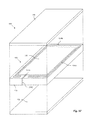
- FIG. 4A is an exploded perspective view of at least a portion of an embodiment of apparatus according to aspects of the present disclosure.
- FIG. 4B is another view of the apparatus shown in FIG. 4A .
- FIG. 4C is a sectional view of the apparatus shown in FIG. 4A .
- FIG. 5A is a top view of at least a portion of an embodiment of apparatus according to aspects of the present disclosure.
- FIG. 5B is a left side view of the apparatus shown in FIG. 5A .
- FIG. 5C is a bottom view of the apparatus shown in FIG. 5A .
- FIG. 5D is a right side view of the apparatus shown in FIG. 5A .
- FIG. 5E is an exploded perspective view of the apparatus shown in FIG. 5A demonstrating a subsequent stage of manufacture according to aspects of the present disclosure.
- FIG. 5F is an exploded perspective view of the apparatus shown in FIG. 5E demonstrating a subsequent stage of manufacture according to aspects of the present disclosure.
- FIG. 5G is a bottom view of an at least a portion of one embodiment of an apparatus according to aspects of the present disclosure, which may be a portion of the apparatus shown in FIGS. 5A-5F .
- FIG. 5H is another perspective view of the apparatus shown in FIG. 5E .
- FIG. 6A is a schematic view of at least a portion of an embodiment of apparatus according to aspects of the present disclosure.
- FIG. 6B is a schematic view of at least a portion of another embodiment of the apparatus shown in FIG. 6A .
- FIG. 7 is a schematic view of at least a portion of an embodiment of apparatus according to aspects of the present disclosure.
- FIG. 8A is a schematic view of another embodiment of the apparatus shown in FIG. 7 .
- FIG. 8B is a schematic view of another embodiment of the apparatus shown in FIG. 7 .
- FIG. 8C is a schematic view of another embodiment of the apparatus shown in FIG. 7 .
- FIG. 8D is a schematic view of another embodiment of the apparatus shown in FIG. 7 .
- FIG. 8E is a schematic view of another embodiment of the apparatus shown in FIG. 7 .
- FIG. 9A is a schematic view of a system and apparatus according to aspects of the present disclosure.
- FIG. 9B is a schematic view an embodiment of apparatus shown in FIG. 9A .
- FIG. 9C is a schematic view an embodiment of apparatus shown in FIG. 9A .
- FIG. 9D is a schematic view an embodiment of apparatus shown in FIG. 9A .
- FIG. 9E is a flow-chart diagram of at least a portion of an embodiment of logic structure according to aspects of the present disclosure.
- FIG. 9F is a flow-chart diagram of at least a portion of an embodiment of logic structure according to aspects of the present disclosure.
- FIG. 9G is a flow-chart diagram of at least a portion of an embodiment of logic structure according to aspects of the present disclosure.
- FIG. 10 is a schematic view of a system and apparatus according to aspects of the present disclosure.
- FIG. 11 is a schematic view of a system and apparatus according to aspects of the present disclosure.
- FIG. 12 is a schematic view of a system and apparatus according to aspects of the present disclosure.
- first and second features are formed in direct contact
- additional features may be formed interposing the first and second features, such that the first and second features may not be in direct contact.
- Exemplary processes which demonstrate the high complexity of interconnecting the individual operations of a multifunction integrated circuit and an energy source become readily apparent when examining the mechanical dimensions of micro- or nano-scale devices designed for substantially autonomous operation.
- integrated circuit feature dimensions e.g., gate widths
- MEMS and other micro-scale devices have reduced in physical size from about 2.0 ⁇ m to today's envisioned 0.35 ⁇ m or smaller.
- feature dimensions are predicted to be as small as about 2 nm, if not smaller.
- microelectronic and other micro-scale devices may have feature dimensions (other than or in addition to thickness) having an order of magnitude of about 1000 ⁇ m or smaller, whereas nanoelectronic and other nano-scale devices have similar feature dimensions having an order of magnitude of about 1000 nm or smaller.
- the lateral dimensions of a microelectronic device feature may be about 500 ⁇ m, whereas the lateral dimensions of a nanoelectronic device feature may be about 500 nm.
- aspects of the present disclosure are not limited to the exemplary definitions of scale described above. Moreover, aspects of the present disclosure may be applicable or readily adaptable to dimensional scales other than the scale employed in discussing such aspects. For example, aspects of micro-scale devices described or otherwise within the scope of the present disclosure may be applicable or readily adaptable to nano-scale devices and devices of other dimensional scale, and aspects of nano-scale devices described or otherwise within the scope of the present disclosure may be applicable or readily adaptable to micro-scale devices and devices of other dimensional scale.
- the present disclosure introduces exemplary embodiments of solid state energy sources for providing operating power to integrated circuit devices.
- aspects of the present disclosure are applicable and/or readily adaptable to apparatus including energy sources integrated with other types of microelectronic devices.
- Such other devices may be or include, without limitation, micro-electro-mechanical (MEMS) devices, nano-electro-mechanical (NEMS) devices, nanotechnology devices, and/or other forms of silicon-based and other semiconductive electronic devices.
- MEMS micro-electro-mechanical
- NEMS nano-electro-mechanical
- an integrated power source within an enclosed package such as with a sensor, an integrated circuit and/or a wireless transmitter/receiver, may allow for vast improvements in the deployment of sensor-based microelectronic devices, and possibly the reconnaissance of information acquisition and communications methods thereof.
- a wireless microelectronic device may be employed in a mobile application, such as to monitor movements of cattle and/or other domesticated or feral animals.
- embodiments within the scope of the present disclosure may provide means for preventing cattle from crossing fences or other boundaries, or from straying into areas where they are not intended.
- Such means may include a microelectronic device attached to an animal, wherein the device may include sensors and possibly utilize a geographic database and/or communications protocol to wirelessly transmit the identity and/or location of the animal to a static “fence-post” unit, which may relay proximity values back to the device.
- the device may wirelessly actuate a mechanism for diverting the motion of the animal beyond a predetermined boundary.
- a device might not be feasible in a rural setting without utilizing an integrated power supply and wireless transmission of data.
- a similar microelectronic device may be utilized in a static or quasi-mobile environment, such as within a hospital room.
- electro-cardio-gram (ECG) devices typically employ electrical sensors to monitor heart rates and waveforms.
- Microelectronic devices can be used to sense these cardiovascular oscillations and wirelessly transmit them back to a peripheral unit for aggregation and processing.
- the peripheral unit may transmit a time-stamp signal to synchronize a plurality of wireless devices that are collectively utilized to constructively and cohesively sense the heart waveform.
- These devices having integrated power sources, need not be linked through a plurality of wires to a power unit, which may greatly reduce the set-up time necessary to wire a patient prior to the performing the ECG procedure, and may also reduce the unpleasant psychological effect of having a plurality of wires connected to a patient.
- the apparatus 100 includes an electrode 110 coupled to a frame 120 .
- the electrode 110 may comprise aluminum, copper, gold, and/or other electrically conductive materials, and may be secured to the frame 120 by adhesive, bonding, brazing, clamps and/or other mechanical fasteners, and/or other means.
- the electrode 110 may have a thickness ranging between about 2 ⁇ m and about 20 ⁇ m. However, other thicknesses are also within the scope of the present disclosure. For example, in an exemplary nano-scale embodiment, the thickness may range between about 10 nm and about 100 nm.
- the frame 120 includes an opening 125 configured to received an energy device according to aspects of the present disclosure.
- the perimeter of the opening 125 may substantially or approximately correspond to a perimeter of a microelectronic device to be coupled to and at least partially powered by the energy device.
- the perimeter of the opening 125 may have a substantially square, rectangular, circular, elliptical, or other regular or irregular geometric shape having lateral dimensions ranging between about 7 nm and about 50 mm.
- the lateral dimensions of the opening 125 may range between about 7 mm and about 9 mm in one implementation, while in another implementation the lateral dimensions of the opening 125 may range between about 1 mm and about 9 mm.
- the opening 125 has a substantially square shape having sides of about 1 mm.
- the frame 120 may be formed by forming the opening 125 in a sheet or plate of frame material, which may comprise one or more ceramics, plastics, and/or other electrically insulating materials.
- the frame material include ceramic, fused silica, and/or silicon carbide, although other materials are also within the scope of the present disclosure.
- the frame 120 may have a thickness ranging between about 0.3 mm and about 0.8 mm, although other thicknesses are also within the scope of the present disclosure. For example, in an exemplary nano-scale embodiment, the thickness may range between about 1 nm and about 20 nm.
- the opening 125 may be one of a plurality of possibly similar openings formed in the frame material, and may be formed in the frame material by micromachining, laser machining, casting, molding, stamping or cutting, and/or or other processes.
- the frame 120 may also comprise more than one layer of materials, including electrically conductive and insulating materials, wherein the multiple layers may be joined in a vertical fashion by adhesive, bonding, welding, and/or other processes.
- the electrode 110 may substantially cover an entire surface of the frame 120 , including the opening formed by the opening 125 . However, in another embodiment, the perimeter of the electrode 110 may more substantially correspond to the perimeter of the opening 125 .
- the frame 120 may also include a shallow recess or other indentation configured to receive the electrode 110 .
- the electrode 110 may be coupled to the frame 120 by press-fitting or otherwise forming an interference or friction engagement between the perimeter of the electrode 110 and the perimeter of the shallow indentation in the frame 120 .
- FIG. 1B illustrated is a sectional view of the apparatus 100 shown in FIG. 1A in which an energy device 130 has been formed or otherwise positioned in the opening 125 .
- An exemplary configuration of the energy stack 130 follows, although other configurations of the energy device 130 are also within the scope of the present disclosure.
- the energy device 130 comprises a separator layer 130 b interposing electrode layers 130 a , 130 c .
- Each of the energy device layers 130 a - c may individually comprise more than one layer, possibly of more than one material.
- the separator layer 130 b may comprise manganese, titanium, vanadium, other solid electrolyte materials, and/or other materials.
- the separator layer 130 b comprises lithium perchlorate (LiClO 4 ) mixed with polyvinylidene (LiClO 4 -PVDF).
- the separator layer 130 b may also or alternatively comprise a lithium salt cross-linked with a polyethyleneoxide.
- the electrode layers 130 a , 130 c form an anode and a cathode of the energy device 130 . That is, the electrode layer 130 a may be an anode of the energy device 130 , and the electrode layer 130 c may be a cathode of the energy device 130 , or the electrode layer 130 a may be a cathode of the energy device 130 , and the electrode layer 130 c may be an anode of the energy device 130 .
- the cathode may comprise dioxide, disulfide, pentoxide, and/or other materials.
- the cathode may also be impregnated with p-type or n-type elemental and/or nano-technology impurities, such as to enhance cathode charging performance and conductivity, possibly depending on the doping scheme employed in the fabrication of the microelectronic device to be packaged with the energy device 130 .
- the anode may be or comprise a metal alloy film or foil that may be impregnated with lithium or lithium alloy impurities.
- the anode may also be impregnated with p-type or n-type elemental and/or nano-technology impurities to enhance anode charging performance and conductivity, possibly depending on the doping scheme employed in the fabrication of the microelectronic device to be packaged with the energy device 130 .
- the cathode may be doped with a first impurity type (e.g., n-type) while the anode may be doped with a second, opposite impurity type (e.g., p-type).
- a first impurity type e.g., n-type
- a second, opposite impurity type e.g., p-type
- the energy device 130 may employ a lithium-manganese-dioxide chemistry, including those which are readily available commercially and/or otherwise understood by those skilled in the art.
- Another example of the energy device 130 chemistry may be lithium-titanium-disulfide (Li—TiSO 2 ) or lithium-vanadium-pentoxide (Li—V 2 O 5 ).
- the cathode and/or anode may be doped with impurities, such as those typically employed in a semiconductor doping scheme. In that regard, the order in which the cathode, anode and separator 130 b are fabricated within the frame 120 may depend on the fabrication processes of the microelectronic device to be packaged with the energy device 130 .
- the cathode may be associated with (or fabricated concurrently with) an n-type semiconductor device substrate or layer and the anode may be similarly associated with a p-type semiconductor substrate or layer.
- the energy device 130 may have a thickness ranging between about 200 ⁇ m and about 1000 ⁇ m, although other thicknesses are also within the scope of the present disclosure.
- the thickness of the energy device 130 may range between about 300 ⁇ m and about 750 ⁇ m, such as about 400 ⁇ m.
- Each of the individual layers forming the energy device layers 130 a - c may have a thickness ranging between about 25 ⁇ m and about 100 ⁇ m.
- the thickness of the energy device 130 may range between about 1 nm and about 20 nm, such as where the thickness of each of the energy device layers 130 a - c is substantially less than about 10 nm.
- the anode may be formed by slicing a rolled lithium foil (possibly comprising battery grade, 99.8% pure lithium) into ingots to approximately 40 ⁇ m in length.
- the anode may also be alloyed with such metals as aluminum, manganese, and/or copper.
- a polymer matrix used by both the separator and cathode material may be formed by emulsifying polymer resin pellets, possibly in combination with a plasticizer.
- the polymer matrix may comprise polyacrylonitrile (PAN), polyvinyliden fluoride (PVdF) and/or polyvinyl sulfone (PVS), and the plasticizer may comprise dibutyl phthalate (DBP).
- the polymer matrix may also comprise one or more polymer additives, possibly including nano-technology derived additives, which may be formulated to enhance a specific operational or performance characteristic.
- the polymer matrix and plasticizer may be emulsified in acetonitrile at about 60° C.
- the resulting viscous solution may then be cast into a polymer substrate to yield a film thickness ranging between about 30 ⁇ m and about 100 ⁇ m.
- the cast polymer membrane film may then be dried, such as in an oven, possibly at a temperature of about 80° C., which may at least partially remove the acetonitrile casting agent.
- the originally highly-viscous membrane may be a translucent, flexible polymer membrane that also contains a high-temperature plasticized structure for rigidity.
- electrolyte components possibly consisting of Ethylenecarbonate-EC, Propylyenecarbonate (PC), and Lithium Perchlorate (LiClO 4 ), mixed in an exemplary ratio of approximately 52/41/7 by weight, respectively, may be used in the preparation of the polymer electrolyte film as described in the above-mentioned emulsification process.
- the electrolyte solution may be heated, possibly to a temperature of about 60° C., and the polymer film may be placed into the heated electrolyte solution, possibly for a period of up to 8 hours, to allow the electrolyte salt to link to the polymer structure.
- the polymer film When the polymer film is removed from the electrolyte solution, it may be cooled to room temperature, which may allow additional electrolyte and polymer cross linking. The resulting solid state electrolyte separator membrane may then be cut to a desirable width and length to complete the separator layer 130 b.
- a similar process may be employed to form the cathode.
- a polymer film employed to form the cathode may have a thickness ranging between about 300 ⁇ m and about 750 ⁇ m.
- the polymer emulsion with plasticizer agent may be mixed with an electrochemical grade of LiMn x O y spinel (FMC-Lithium) and a Super-P carbon such as Vulcan XC-72 (Cabot).
- a mixture of polyethylene oxide containing high-temperature plasticizers, LiMnO 2 spinel (FMC-Lithium) and Super-P carbon (Vulcan-XC-72 Cabot) may be used in a ratio of approximately 55/42/3 by weight, respectively.
- the resulting polymer film may then be cut to a desirable width and length to form the cathode.
- the energy device layers 130 a - c may be formed or otherwise positioned in the frame 130 by pressing the individual or stacked layers into the opening 125 .
- the energy device layers 130 a - c may be cut-to-size prior to positioning in the opening 125 , or may be trimmed after, or as a result of, their installation into the opening.
- the energy device layers 130 a - c may be individually or collectively compressed during or after their installation into the opening 125 .
- the energy device layers 130 a - c may be subjected to a compression force ranging between about 10 psi (69 kPa) and about 200 psi (1379 kPa).
- the compression force ranges between about 30 psi (207 kPa) and about 50 psi (349 kPa), such as about 40 psi (279 kPa).
- the energy device layers 130 a - c may be compressed until a desired thickness is achieved. Alternatively, or additionally, the energy device layers 130 a - c may be compressed until a desired output current is achieved from a given voltage.
- FIG. 1C illustrated is a sectional view of the apparatus 100 shown in FIG. 1B in which an additional electrode 140 has been coupled to the frame 120 and/or the energy device 130 . Consequently, the energy device 130 may be sandwiched between and possibly directly contact each of the electrodes 110 , 140 .
- the electrode 140 may be substantially the same as the electrode 110 , and may be secured to the frame 120 and/or the energy device 130 in substantially the same manner, or via one of the other securing means described above regarding the attachment of the electrode 110 to the frame 120 .
- the compression process described above may be performed after the electrode 140 has been secured to the frame 120 and/or the energy device 130 , either in addition to or in the alternative to performing the compression process after the energy device 130 is formed in the frame 120 .
- the above-described manufacturing process for fabricating the apparatus 100 may also include verifying a maximum relative flatness and/or parallelism of the electrodes 110 , 140 .
- the compression process described above may be performed sufficiently to achieve maximum flatness and/or minimum variation in parallelism of the electrodes 110 , 140 of about 5 ⁇ m or less.
- FIG. 2A illustrated is a sectional view of at least a portion of an embodiment of the apparatus 100 shown in FIG. 1A , herein designated by numeral reference 100 A.
- the apparatus 100 A is substantially similar to the apparatus 100 shown in FIG. 1A , although the apparatus 100 A includes multiple instances of the frame 120 , the energy device 130 , and the electrodes 110 , 140 .
- a sheet or plate of frame material 120 A having openings 125 formed therein is secured to an electrode sheet 110 A
- the frame material 120 A and electrode sheet 110 A may each be substantially similar in composition and manufacture to the frame 120 and electrode 110 , respectively, shown in FIGS. 1A-1C .
- the electrode sheet 110 A and the frame material 120 A may also be secured to one another in a manner similar to the attachment of the frame 120 and the electrode 110 discussed above.
- the electrode sheet 110 A may comprise a single continuous sheet or more than one sheet each corresponding to one or more of the openings 125 .
- FIG. 2B illustrated is a sectional view of the apparatus 100 A shown in FIG. 2A in which an energy device 130 has been formed in each of the openings 125 in the frame material 120 A.
- Each of the energy devices 130 shown in FIG. 2B may be substantially similar to the energy device 130 shown in FIGS. 1B, 1C .
- the energy devices 130 may be individually or collectively compressed, such as by the compression processes described above.
- the sequence by which the energy devices 130 are assembled in the openings 125 is not limited within the scope of the present disclosure.
- a first energy device layer 130 a may be formed in a corresponding opening 125
- a second energy device layer 130 b may then be formed in the opening 125
- a third energy device layer 130 c may be formed in the opening 125 , then this process may be repeated for each remaining opening 125 , individually.
- the first energy device layer 130 a may be formed in each of the openings 125
- the second energy device layer 130 b may be formed in each of the openings 125
- the third energy device layer 130 c maybe formed in each of the openings 125 .
- a sheet of first energy device layer material may be dispensed as a liquid into the frame, or as a solid sheet placed over the frame material 120 A and punched, pressed or otherwise positioned in each of the openings 125 , such as by a die or roller, and a similar process may be repeated for each of the remaining energy device layers.
- Each of the layers forming an energy device 130 may alternatively be pre-assembled to one another to form an energy device layer stack. Thereafter, the layer stack may be formed in each of the openings 125 one at a time, or the layer stack may be formed in each of the openings 125 substantially simultaneously.
- a roller or die press having bosses substantially corresponding to the shape and position of the openings 125 may be employed to position portions of the layer stack into corresponding openings 125 .
- FIG. 2C illustrated is a sectional view of the apparatus 100 A shown in FIG. 2B in which an additional electrode sheet 140 A has been secured to the frame material 120 A and/or each of the energy devices 130 .
- the electrode sheet 140 A may be substantially similar in composition and manufacture to the electrode 110 shown in FIGS. 1A-1C .
- the electrode sheet 140 A may also be secured to the frame material 120 A and/or the energy devices 130 in a manner similar to the attachment of the electrode 140 to the frame 120 discussed above.
- the electrode sheet 140 A may comprise one continuous sheet or more than one sheet each corresponding to one or more of the openings 125 .
- the compression process described above may also be performed after the electrode sheet 140 A has been secured to the frame material 120 A and/or the energy devices 130 , either in addition to or in the alternative to performing the compression process after the energy devices 130 are formed in the openings 125 .
- the apparatus 100 A may be substantially configured to provide energy to one or more devices to be packaged with the apparatus 100 A.
- Portions of the electrode sheets 110 A, 140 A may be removed to separate one or more of the energy devices from one another.
- two or more adjacent energy devices 130 may remain interconnected by portions of one or both of the electrode sheets 110 A, 140 A and/or frame material 120 , such as where the energy requirements for a particular device packaged therewith are greater than the capacity of each individual energy device 130 .
- Such an embodiment may be advantageous when a standard energy device 130 may be desired.
- the layers employed as anode and cathode layers in some of the energy devices 130 may need to be reversed.
- FIG. 2D illustrated is a sectional view of the apparatus 200 shown in FIG. 2C in which individual apparatus 100 B have been formed from the apparatus 100 A by dicing or otherwise removing portions of the electrode sheets 110 A, 140 A and/or frame material 120 A.
- Each of the apparatus 100 B may be substantially similar to the apparatus 100 shown in FIG. 1C .
- Two or more of the apparatus 100 B may also be stacked in a single package, such as to provide additional energy capacity.
- one or both of the electrode sheets 110 A, 140 A interposing two vertically stacked energy devices 130 may be removed.
- the apparatus 200 A includes an energy cell 210 that may be substantially similar to the apparatus 100 shown in FIG. 1C , one of the apparatus 100 B shown in FIG. 2D , and/or one of the energy devices 130 shown in FIG. 1B, 1C , or 2 B- 2 D.
- the apparatus 200 A also includes a device 220 to be at least partially powered by the energy cell 210 .
- An interface layer 230 may comprise or at least partially provide one or more interfaces between the energy cell 210 and the device 220 .
- aspects of the present disclosure are also applicable and/or readily adaptable to other embodiments of the apparatus 200 A which may include more than one energy cell 210 , more than one device 220 , and/or more than one interface layer 230 .
- the multiple energy cells 210 may or may not be substantially identical
- the multiple devices 220 may or may not be substantially identical
- the multiple interface layers 230 may or may not be substantially identical.
- the device 220 may be or comprise one or more integrated circuit devices, micro-electromechanical (MEMS) devices, nano-electromechanical (NEMS) and other nano-scale devices, organic electronic devices, other microelectronic devices, sensor devices, RFID devices, and/or a variety of combinations thereof.
- the device 220 may additionally or alternatively comprise a plurality of transistors, capacitors, inductors, analog signal processing devices, memory devices, logic devices, and/or other microelectronic devices interconnected by, for example, a plurality of electrically conductive vias, landing pads, and/or other forms of electrically conductive interconnects.
- Several of such devices and interconnects are collectively designated by reference numeral 222 in FIG. 3 .
- the device 220 may be any device having electrically conductive contacts 225 configured for connection with an energy source. Such devices may be formed on and/or in a substrate 227 substantially comprising silicon, or a variety of other semiconductor materials, and/or a variety of other substrate suitable materials.
- a device having such a substrate 227 may include electrically conductive contacts, vias or other electrically conductive members 225 extending at least partially into or through the substrate 227 to a bottom or other surface for interconnection with the energy cell 210 via the interface layer 230 .
- the conductive members 225 may electrically couple the energy cell 210 , at least indirectly, with one or more of the individual devices which compose the device 220 .
- the device 220 may also or alternatively include or otherwise be electrically interconnected by wire bonds to the energy cell 210 .
- the device 220 may also or alternatively be electrically connected to the energy cell 210 via the interface layer 230 by flip-chip mounting or other processes employing stud bumps, solder balls, and/or electrically conductive epoxy or other adhesives.
- the interface layer 230 may comprise one or more layers of various electrically conductive and/or electrically insulating materials.
- the interface layer 230 comprises a number of electrically conductive members 235 configured to interconnect contacts 225 of the device 220 with the energy cell 210 .
- the electrically conductive members 235 may comprise aluminum, copper, gold, tungsten, conductive epoxy and other electrically conductive adhesives, solder, and/or other materials.
- Gaps 237 between the conductive members 235 may substantially comprise air, inert gases (e.g., argon), a vacuum, and/or dielectric materials such as silicon dioxide, fluorinated silicate glass (FSG), SILK (a product of Dow Chemical), or Black Diamond (a product of Applied Materials).
- inert gases e.g., argon
- dielectric materials such as silicon dioxide, fluorinated silicate glass (FSG), SILK (a product of Dow Chemical), or Black Diamond (a product of Applied Materials).
- the interface layer 230 may also be or at least partially comprise a flag, paddle, central support member or other portion of a lead frame employed to interconnect power and/or data contacts of the device 220 with surrounding circuitry.
- lead frame portion may alternatively be positioned elsewhere besides interposing the energy cell 210 and the device 220 .
- the energy cell 210 may interpose and possibly contact both the lead frame and the device 220
- the device 220 may interpose and possibly contact both the lead frame and the energy cell 210 .
- the contact between the energy cell 210 , the device 220 and/or the lead frame may be through one or more intermediary layers, such as may be employed to improve adhesion, electrical conductivity and/or electrical isolation between the “contacting” components.
- the apparatus 200 A may also include a manufacturing process handling or transport substrate or other structure coupled to the energy cell 210 (hereafter referred to as the handle 240 ), such as in the illustrated example.
- the handle 240 may assist in the handling of the apparatus 200 A during and/or after manufacturing.
- the apparatus 200 A may not include the handle 240 . Nonetheless, when the handle 240 is employed, it may be removed and possibly discarded during or after manufacturing.
- the handle 240 may also be positioned relative to the other features of the apparatus 200 A in locations other than as shown in FIG. 3A .
- the handle 240 may be coupled to the device 220 rather than to the energy cell 210 .
- the handle 240 may also be employed during the manufacture and/or assembly of the feature to which it is coupled.
- the handle 240 may be integral to or otherwise coupled to the energy cell 210 or the device 220 during the manufacture and/or assembly thereof.
- the apparatus 200 A may also include a sacrificial or release layer 245 interposing the handle 240 and the remainder of the apparatus 200 A.
- the sacrificial layer 245 may comprise silicon dioxide, polysilicon, and/or other materials easily removable by a diluted hydrofluoric acid etch and/or other conventional or future-developed sacrificial layer removal processes.
- the sacrificial layer 245 may also or alternatively comprise an adhesive which may permanently or temporarily bond the handle 240 to the energy cell 210 or other portion of the apparatus 200 A. Clamps and/or other mechanical fasteners may be employed in addition to or in the alternative to the sacrificial layer 245 .
- the apparatus 200 A may also include or be encapsulated in one or more insulating layers formed around a substantial portion of the apparatus 200 A, such as to protect the apparatus 200 A from potentially hazardous mechanical and environmental elements which may cause damage or destruction.
- encapsulating or insulating layer(s) may comprise polyphenolene sulfide and/or a variety of another non-conductive encapsulant materials
- FIG. 4A illustrated is an exploded perspective view of at least a portion of an embodiment of an apparatus 300 according to aspects of the present disclosure.
- the portion of the apparatus 300 shown in FIG. 4A includes an energy cell 310 having an energy device 130 formed or otherwise positioned in a frame 120 , as well as electrodes 110 , 140 .
- the energy cell 310 may be substantially similar to the apparatus 100 shown in FIG. 1C and/or the apparatus 100 B shown in FIG. 2D .
- a portion of the energy device 130 and the frame 120 have been removed and the electrodes 110 , 140 are shown in a disassembled configuration.
- the frame 120 may include an electrically conductive via or other conductive member 320 extending through the frame 120 .
- the perimeter of the electrode 140 may also include a scallop, recess, indentation, or otherwise defined profile 325 configured such that the electrode 140 does not electrically contact the conductive member 320 when the electrode 140 is coupled to the frame 120 , such as in the assembled configuration of the energy cell 310 shown in the perspective view in FIG. 4B .
- FIG. 4C illustrated is a sectional view of the apparatus 300 shown in FIG. 4A in which the energy cell 310 and a device 220 to be packaged with the energy cell 310 have been coupled via an interposing member 330 .
- the device 220 may be substantially similar to the device 220 discussed above with reference to FIG. 3 .
- the interposing member 330 may be or comprise at least a portion of a paddle, flag, and/or other portion of a lead frame.
- a lead frame may be a conventional or future-developed lead frame assembly having an industry-standard geometry and composition.
- the lead frame assembly may include a paddle, flag, or other central support member and a plurality of formable, flexible metal leads that extend radially around the periphery of the central support member to a plurality of “J” style leads or other end use, packaging style appropriate pin connectors.
- the lead frame assembly may include 28 pairs of leads and connectors, such as the Olin Brass C194 distributed by A.J. Oster Company of Warwick, R.I.
- the central support member may also include a conductive coating on one or both major surfaces thereof to increase their electrical conductivity.
- a conductive coating may be or comprise a graphite based coating having a thickness of about 25 ⁇ m, such as Electrodag® EB-012 distributed by the Acheson Colloids Company of Port Huron, Mich.
- the conductive coating may be applied by lamination or conventional or future-developed thin-film deposition processes, and may be cured by exposure to heat or air, for example.
- the energy cell 310 and the device 220 may each be coupled to the interposing member 330 via one or more adhesive layers 340 .
- the adhesive layers 340 may each comprise an electrically and/or thermally conductive elastic dry film and/or a silicone elastomer, possibly including a silver pigmentation.
- the energy cell 310 and the device 220 may also or alternatively be welded to the interposing member 330 by laser welding and/or other conventional processes.
- the apparatus 300 may also include a plurality of wire bonds 350 or other type of conventional or future-developed interconnection media, such as those comprising carbon nanotubes or polyacetalynes.
- Each wire bond 350 couples a lead or other portion of the interposing member 330 to corresponding bond pads or other contacts formed on and/or in the device 220 .
- the wire bonds 350 may be employed for power supply voltages, regulated power conditioned and battery charging voltages, analog conditioning and sensing signals, micro-electromechanical sensing and activation signals, digital input/output signals, such as chip select, addressing or data signals, and/or other signals between the device 220 and circuitry connected to the interposing member 330 .
- An additional wire bond 355 may couple one of the bond pads or other contacts formed on and/or in the device 220 to the conductive member 320 .
- the wire bond 355 may be substantially similar in composition, manufacture, and assembly to the wire bond 350 .
- the wire bond 355 may extend through an opening, gap, or other aperture 335 in the interposing member 330 , or may be routed around the perimeter of the interposing member 330 .
- the wire bonds 350 , 355 may comprise gold and/or other conductive materials, and may be formed and assembled by conventional and/or future-developed processes.
- the device 220 may be connected to the electrode 110 via the wire bond 355 .
- the device 220 may also be connected to the electrode 140 of the energy device 310 by an additional wire bond or other similarly described 350 connection means discussed above.
- the device 220 is connected to the electrode 140 via the interposing member 330 and the adhesive layers 340 .
- a power supply contact for the device 220 may be on a surface of the device 220 that is contacted by one of the adhesive layers 340 (e.g., the lower surface in the orientation shown in FIG.
- the adhesive layers 340 and the interposing member 330 collective connect the power supply contact of the device 220 to the electrode 140 of the energy device 310 , wherein the electrode 140 may be an anode of the energy device 310 , or may be connected to the anode of the energy device 310 . Consequently, the cathode of the energy device 310 , which may be the electrode 110 , or which may be connected to the electrode 110 , may be connected to a ground potential contact for the device 220 through the conductive member 320 and the wire bond 355 .
- aspects of the apparatus 300 are applicable and/or readily adaptable to embodiments employing energy cells other than the energy cell 310 , and also to embodiments employing devices other than the device 220 described herein. Some embodiments of the apparatus 300 may also include more than one energy cell, each of which may be substantially similar to or different than the energy cell 310 , and may also include more than one device, each of which may be substantially similar to or different than the device 220 .
- the apparatus 300 shown in FIG. 4C may also exclude one or both of the electrodes 110 , 140 .
- the interposing member 330 may be coupled directly to the topmost (relative to the orientation shown in FIG.
- the bottommost layer of the energy device 130 may be connected to the conductive member 320 directly or by one or more elements, features, components, or members other than the electrode 110 .
- FIG. 5A illustrated is a top view of at least a portion of an embodiment of the frame 120 discussed above and designated herein by the reference numeral 500 .
- the frame 500 is substantially similar in composition and manufacture to the frame 120 discussed above, and includes an opening 502 configured to receive an energy device stack, such as that comprising the energy device layers 130 a - c described above.
- the frame 500 also includes traces, metallization features, and/or other electrically conductive members herein referred to as conductive members 510 (the frame 120 described above may include similar conductive members 510 ).
- the electrically conductive members 510 may comprise aluminum, copper, gold, tungsten, and/or other conductive materials, and may be formed by selective deposition or bonding, brazing, blanket deposition following by one or more patterning processes, and/or other processes.
- the electrically conductive members 510 may have a thickness ranging between about 50 ⁇ m and about 500 ⁇ m, although a variety of other thicknesses are also within the scope of the present disclosure.
- the electrically conductive members 510 are illustrated as being recessed within the surfaces of the body 505 of the frame 500 , such that the upper or outer surfaces or profiles of the electrically conductive members 510 may be substantially planar or recessed within the body surface in which the conductive members 510 are formed.
- the electrically conductive members 510 may be formed by forming recesses in the frame body 505 , such as by etching, laser machining, and/or other processes, and subsequently filling the recesses with conductive material, possibly followed by one or more chemical-mechanical polishing or planarizing processes and/or other planarizing processes.
- the electrically conductive members 510 may be only partially recessed within the surfaces of the frame body 505 , thereby at least partially protruding from the surfaces of the body 505 .
- the surfaces of the body 505 may be substantially planar and the electrically conductive members 510 may merely be formed thereon.
- the electrically conductive members 510 include a electrically conductive member 510 A which comprises one or more perimeter portions substantially surrounding the opening 502 or otherwise configured to contact an electrode component coupled to the frame 500 and/or an outermost energy device layer located in the opening 502 adjacent the electrically conductive member 510 A.
- the electrically conductive member 510 A also includes one or more extension portions 511 A extending between the perimeter portions thereof and a spanning conductive member 510 C shown more clearly in FIG. 5B .
- the electrically conductive members 510 also include a conductive member 510 B which comprises one or more perimeter portions substantially surrounding the opening 502 but electrically isolated from the electrically conductive member 510 A, such as by a gap 515 comprising air, inert gases, other dielectric materials, or a vacuum.
- the conductive member 510 B may substantially or at least partially conform to the electrically conductive member 510 A, although the conductive member 510 B may be offset radially outward from the conductive member 510 A. Ends 512 of the conductive member 510 B may terminate on opposing sides of the extension portion 511 A of the electrically conductive member 510 A.
- the conductive member 510 B may also include one or more extension portions 511 B extending between the perimeter portions thereof and an additional spanning conductive member 510 D shown more clearly in FIG. 5D .
- the extension portions 511 A, 511 B of the electrically conductive members 510 A, 510 B may be located at opposite, possibly substantially parallel ends or sides of the frame 500 , as shown in FIG. 5A , although in other embodiments the extension portions 511 A, 511 B of the electrically conductive members 510 A, 510 B may be located on adjacent, possibly perpendicular ends or sides of the frame 500 .
- the spanning conductive member 510 C includes one or more portions collectively or each individually spanning the thickness of the frame body 505 , thereby connecting the extension portion 511 A of the electrically conductive member 510 A and an additional conductive member 510 E shown more clearly in FIG. 5D .
- the spanning conductive member 510 D includes one or more portions collectively or each individually spanning the thickness of the frame body 505 , thereby connecting the extension portion 511 B of the electrically conductive member 510 B and an additional conductive member 510 F shown more clearly in FIG. 5D .
- the electrically conductive members 510 include conductive member 510 F which comprises one or more perimeter portions substantially surrounding the opening 502 or otherwise configured to contact an electrode component coupled to the frame 500 and/or an outermost energy device layer located in the opening 502 adjacent the conductive member 510 F.
- the conductive member 510 F also includes one or more extension portions 511 F extending between the perimeter portions thereof and the spanning conductive member 510 D shown more clearly in FIG. 5C .
- the electrically conductive members 510 also include conductive member 510 E which comprises one or more perimeter portions substantially surrounding the opening 502 but electrically isolated from the conductive member 510 F, such as by a gap 517 comprising air, inert gases, other dielectric materials, or a vacuum.
- the conductive member 510 E may substantially or at least partially conform to the conductive member 510 F, although the conductive member 510 E may be offset radially outward from the conductive member 510 F. Ends 514 of the conductive member 510 E may terminate on opposing sides of the extension portion 511 F of the conductive member 510 F.
- the conductive member 510 E may also include one or more extension portions 511 E extending between the perimeter portions thereof and the spanning conductive member 510 C shown more clearly in FIG.
- the extension portions 511 E, 511 F of the conductive members 510 E, 510 F may be located at opposite, possibly substantially parallel ends or sides of the frame 500 , as shown in FIG. 5D , although in other embodiments the extension portions 511 E, 511 F of the conductive members 510 E, 510 F may be located on adjacent, possibly perpendicular ends or sides of the frame 500 .
- the spanning conductive member 510 C may comprise more than one laterally offset member each spanning the left side of the frame body 505 , although such a configuration may also require that the electrically conductive members 510 A, 510 E each comprise more than one extension portion extending from their respective perimeter portions.
- the spanning electrically conductive member 510 D may comprise more than one laterally offset member each spanning the right side of the frame body 505 , although such a configuration may also require that the electrically conductive members 510 B, 510 F each comprise more than one extension portion 511 B, 511 F extending from their respective perimeter portions.
- the patterns of the electrically conductive members 510 A, 510 F may be substantially identical or similar, or mirror images, depending upon the orientations employed for such a comparison.
- the patterns of the electrically conductive members 510 B, 510 E may be likewise similar, as well as the patterns of the conductive members 510 C, 510 D.
- FIG. 5E illustrated is an exploded perspective view of at least a portion of an embodiment of an apparatus 550 according to aspects of the present disclosure.
- the apparatus 550 is one environment in which the frame 500 shown in FIGS. 5A-5D may be implemented.
- the portion of the apparatus 550 shown in FIG. 5E includes an energy cell 560 having an energy device (such as energy device 130 described above) formed or otherwise positioned in the frame 500 , as well as electrodes 110 , 140 on opposing sides of the energy device.
- the energy cell 560 may be substantially similar to the apparatus 100 shown in FIG. 1C and/or the apparatus 100 B shown in FIG. 2D .
- the electrodes 110 , 140 may be coupled or otherwise secured to the frame 500 by Nd:YAG laser soldering or active brazing. However, for the sake of clarity, the electrodes 110 , 140 are shown in a disassembled configuration in FIG. 5E .
- the perimeter of the electrode 140 may substantially conform or otherwise correspond to the electrically conductive member 510 A shown in FIG. 5A , or at least to the perimeter portions of the electrically conductive member 510 A (e.g., excluding the extension portion 511 A). Accordingly, upon assembly, the electrode 140 may electrically contact a substantial portion of the conductive member 510 A and/or an electrode layer or other outermost layer of the energy cell 560 . However, the perimeter of the electrode 140 may also be offset laterally inward relative to the electrically conductive member 510 B shown in FIG. 5A , such that electrode 140 may be electrically isolated from the electrically conductive member 510 B. Otherwise, the electrode 140 may substantially be as described above.
- the perimeter of the electrode 110 may substantially conform or otherwise correspond to the electrically conductive member 510 F shown in FIG. 5D , or at least to the perimeter portion of the electrically conductive member 510 F (e.g., excluding the extension portion 511 F). Accordingly, upon assembly, the electrode 110 may electrically contact a substantial portion of the electrically conductive member 510 F and/or an electrode layer or other outermost layer of the energy cell 560 . However, the perimeter of the electrode 110 may also be offset laterally inward relative to the electrically conductive member 510 E shown in FIG. 5D , such that electrode 110 may be electrically isolated from the electrically conductive member 510 E. Otherwise, the electrode 110 may substantially be as described above.
- FIG. 5F illustrated is an exploded perspective view of at least a portion of an embodiment of an apparatus 555 according to aspects of the present disclosure.
- the apparatus 555 is one environment in which the apparatus 550 shown in FIG. 5E may be implemented.
- the portion of the apparatus 555 shown in FIG. 5F includes an embodiment of the apparatus 550 , or another type of energy cell or energy storage device, as well as devices 570 , 580 to be packaged on opposing sides of the apparatus 550 .
- the devices 570 , 580 are shown in a disassembled configuration in FIG. 5F .
- the devices 570 , 580 may be substantially similar to the devices 220 or other devices described above as being packaged with an energy device or cell.
- the apparatus 555 may also include only one of the devices 570 , 580 .
- one or more of the electrodes 110 , 140 shown in FIG. 5E , and/or one or more of the conductive members 510 shown in FIGS. 5A-5D may be omitted.
- the electrode 110 shown in FIG. 5E may be omitted.
- I/O contacts 571 may, for example, be constructed utilizing flip-chip evaporated Under Bump Metallization (UBM) and conductive adhesive stencil techniques.
- UBM Under Bump Metallization
- a large area single contact point 572 or a plurality of multiple contact points can similarly be formed utilizing similar techniques.
- the device 570 / 580 For assembly of the device 570 / 580 to the assembled power source (e.g., apparatus 550 shown in FIG. 5E ), the device 570 / 580 is flipped on top of the cell assembly 550 such that the I/O contacts 571 align with the metallized and electrically conductive member 510 B or 510 E. Contact for the large area contact points within the center of the die can be accomplished anywhere on the electrode element 110 or 140 .
- a complimentary construction technique can be utilized for assembly of a second device 570 / 580 where its associated I/O contacts align with and contact the corresponding conductive member 510 B or 510 E and its associated center contact 572 aligns with and contacts the corresponding electrode element 110 or 140 .
- each of the three assembled devices now consisting of an energy storage cell 550 layered between two devices 570 / 580 , may be temporarily held together using an assembly tape such as Kapton® (I.E. DuPont) until an interposing, conductive adhesive can be cured, such as at about 150° C. for fifteen to thirty minutes.
- assembly tape such as Kapton® (I.E. DuPont) until an interposing, conductive adhesive can be cured, such as at about 150° C. for fifteen to thirty minutes.
- aspects of the apparatus 500 , 550 , 555 are applicable and/or readily adaptable to embodiments employing energy cells other than those shown in FIGS. 5A-5G , and also to embodiments employing devices other than the devices shown in FIGS. 5A-5G or otherwise described herein.
- Embodiments of the apparatus 500 , 550 , 555 may also include more than one energy cell, each of which may be substantially similar to or different than those shown and described herein, and may also include more than one device, each of which may be substantially similar to or different than the devices shown and described herein.
- FIG. 5H illustrated is a perspective view of the apparatus 555 shown in FIG. 5F after the devices 570 / 580 have been assembled to opposing surfaces of the energy storage cell 550 .
- the footprint of each of the devices 570 / 580 substantially conforms to the footprint of the energy storage cell 550 , both in regard to shape and surface area.
- one or both of the devices 570 / 580 may alternatively have a footprint that differs in shape and/or surface area relative to the footprint of the cell 550 , whether or larger or smaller.
- the apparatus 600 A includes a device 610 packaged with and powered at least partially by an energy storage device 620 according to aspects of the present disclosure.
- the device 610 may be substantially similar to the device 220 described above, other devices described herein, and/or other devices within the scope of the present disclosure.
- the device 220 may also include more than one discrete device, die, or chip, or may itself be or comprise an apparatus substantially similar to the apparatus 600 A.
- the energy storage device 620 may be substantially similar to one or more of the energy devices or cells described above. However, rather than merely generating the energy provided to at least partially power the device 610 , the energy storage device 620 is also electrically coupled to an energy source 630 , such as by wires or other electrically conductive members 640 , which may be configured to recharge the energy storage device 620 .
- the energy source 630 may be or include a nuclear battery, such as described in “The Daintiest Dynamos,” IEEE Spectrum, September 2004, Amit Lal and James Blachard, the entirety of which is hereby incorporated by reference herein.
- the energy source 630 may additionally or alternatively be or include a MEMS based thin-film fuel cell, such as described in U.S. Pat. No. 6,638,654 to Jankowski, et al., the entirety of which is hereby incorporated by reference herein.
- the energy source 630 may additionally or alternatively be or include RF energy collectors similar to RFID Tag and Electronic Product Code (EPC) implementations, such as described in Technology Review, July/August 2004, pp 74, 75, Erika Joniets, Massachusetts Institute of Technology (MIT), the entirety of which is hereby incorporated by reference herein.
- the energy source 630 may additionally or alternatively be or include a single or plural configuration of photovoltaic cells, such as described in U.S. Pat. No. 6,613,598 to Middelman, et al., U.S. Pat. No. 6,580,026 to Koyanagi, et al., U.S. Pat. No. 6,538,194 to Koyanagi, et al., U.S. Pat.
- the energy source 630 may additionally or alternatively be or include one or more of: a radioactive generator, a ferro-electric or magnetic generator, a lead zirconate titanate (PZT) electricity generating ceramic device, or a MEMs based petro-chemical internal combustion engine with an electric generator, an elastomeric generator, or a piezoelectric generator, or other acoustic or mechanical vibration piezoelectric energy harvesters, among others.
- a radioactive generator a ferro-electric or magnetic generator
- PZT lead zirconate titanate
- FIG. 6B illustrated is a schematic view of at least a portion of another embodiment of the apparatus 600 A shown in FIG. 6A , herein designated by the reference numeral 600 B.
- the apparatus 600 B may be substantially similar to the apparatus 600 A, except that the energy source 630 may be directly coupled to the energy storage device 620 in the apparatus 600 B.
- the energy source 630 may be coupled to the energy storage device 620 by one or more layers which may be substantially similar to the interface layer 230 and/or the adhesive layers 340 described above. Consequently, the energy source 630 may be adjacent to or otherwise centrally located with the energy storage device 620 , whereas the energy source 630 may be located remote from the energy storage device 620 in the apparatus 600 A shown in FIG. 6A .
- an integrated ESD device includes security keys, locks and ignition systems, automobile-body-mounted crash sensors, tire air pressure sensors, or consumable product status sensors and indicators, among others.
- One example is a device employed with a typical automotive air intake line, where a low cost air-pressure sensor which measures air pressure can be utilized to indicate the volume of airflow into the carburetor.
- a contaminated or failing air filter may yield a measurable increase in air intake pressure from a known airflow operating condition, which may be empirically measured if a sensor is physically located on an air intake path or manifold just past the air filter element.
- a single integrated package containing a MEMS type of pressure sensor, an ESD rechargeable battery, and a MEMS based kinetic power source, all collocated and encapsulated or otherwise integrally packaged into an automotive-ergonomic compatible package may be placed on an air inlet hose or manifold located in a position following the air filter but in front of the carburetor (or other air inlet to the engine).
- An autonomous, self-powered pressure sensor of this type may give indication to the vehicle owner/operator of a filter-replacement requirement, such as via illumination of a light emitting diode (LED).
- LED light emitting diode
- military applications for an integrated ESD type of device include countermeasure devices such as infrared chafes, smart munitions on small caliber munitions rounds, anti-fuse based solid state detonators, or consumable chemical or biological agent detectors.
- countermeasure devices such as infrared chafes, smart munitions on small caliber munitions rounds, anti-fuse based solid state detonators, or consumable chemical or biological agent detectors.
- a contemporary military aircraft countermeasure to an adversarial firing of a heat-seeking or infrared-guided missile is the use of infrared (IR) generating chafes.
- IR infrared
- the chafe is a small device typically containing a hydrocarbon-based fuel that, when ignited, burns hot enough to give off an emission of thermal infrared energy.
- This infrared energy signature is intended to be of sufficient luminescent quantity, and of sufficient time duration, to duplicate the energy signature of the aircraft jet engine.
- the diversionary and decoy properties of the deployed chafes cause the heat-seeking guidance system of the adversarial missile to become confused as to which glowing object is the targeted aircraft engine.
- the infrared signature of the chafes becomes more predominate than the IR emission signature of the targeted jet engine, and the missile subsequently follows the new, brighter signature of the decoy chafes.
- This diversionary and decoy mechanism of substituting the infrared signature of chafes for the infrared signature of targeted jet engines is an effective countermeasure in a threatening and potentially lethal situation where both the aircraft and its pilot avoid the catastrophe of being destroyed by an adversary's guided missile.
- the chafes are typically a fueled, pyrotechnic device.
- An ESD-based intelligent chafe, constructed according to aspects of the present disclosure, may be produced in virtually any favorable airborne geometry.
- each chafe disk may be configured to contain an ESD type of device which allows for a delayed-fuse activation of a high-intensity, infrared light emitting source.
- each chafe disk may contain one, two or more conductive elements that, when aligned into a launching cylinder, are utilized to electronically activate the infrared emitting source on the disk.
- the chafes When stacked in numbers and aligned in a firing cylinder, the chafes can be launched or propelled from the cylinder when activated.
- Potential benefits of utilizing this method of countermeasure include the geometric coverage area of the infrared signature left behind the targeted aircraft by the launched chafes, their programmable timing for activation delay from launch, their illumination duration, and their intensity of the infrared emission in each chafe.
- Industrial applications of ESD based devices include a variety of autonomous transducers and sensors, as well as manufacturing tracking, shipping, and product authenticity implementations.
- one implementation may entail products which are manufactured utilizing highly-automated assembly processes, such as those processes which are substantially automated from beginning to end, including where an assembly process progresses with the insertion of various subassemblies into a manufacturing process carrier or tray.
- the carrier or tray will be referred to hereafter as a “handler.”
- a variety of sensors located within the conveyor system or assembly station of an assembly process may be utilized as quality-feedback mechanisms, such as to ensure that each process step is concluded with the desired result.
- the sensors may allow the product to be either accepted and forwarded to the next assembly stage, or to be rejected from the assembly process entirely.
- Yield is a percentage calculation indicative of a ratio measure of the amount of product (e.g., production units) that are accepted through each process stage divided by the total number of units that started through the process stage.
- the desired outcome may be to keep the automated process within sufficient quality parameters that the yield metric remains as high as possible.
- the handler may be created such that it may contain an intelligent measurement and communications device whereby the assembly performance results of each stage of the manufacturing process can be acquired and stored.
- An integrally-packaged ESD device may be molded or mounted into the handler.
- the device may contain a single or series of integrated circuits comprising, for example, a micro- and/or nano-technology-based, articulated MEMS- or NEMS-based gyroscope to detect assembly orientation.
- the device may contain a multi-function microcontroller interface that is capable of analog sensing, such as may be configured to sense temperature.
- the microcontroller may additionally be configured to perform conversion of the analog sensing signal into digital data, and the microcontroller or other portion of the device may also include memory for the storage of the digital data.
- the handler may hold the assembly for a spray deposition process in such a way that robotic orientation of the device must be measured within six degrees of freedom, for specific amounts of time, and at specific spray deposition temperatures.
- a high-temperature curing process may involve similar actuation of the handler in six degrees of freedom and with specific amounts of time at specific curing temperatures.
- the integrated circuit of the integrated ESD device package may be activated through the use of a magnetic Hall Effect transistor, for example.
- the microcontroller may begin to sense signals from the MEMS gyroscope and/or the temperature sensor and, possibly with each measurement cycle, store the results of the measurement within a static random access memory of the microcontroller or other portion of the integrated ESD device.
- the handler may proceeds through the spray deposition stage followed by the high-temperature curing stage.
- data indicative of the condition of the handler orientation and temperature may be collected and/or stored in the integrated ESD device of the present disclosure.
- the handler may be exposed to an RF field within sufficient proximity to allow for the initiation and transfer of data from the integrated ESD device of the handler to a process controller.
- the process controller may read the digitally encoded data and, possibly through the use of the aforementioned Hall Effect switch, turn off or otherwise deactivate the integrated ESD device. With the data from the integrated ESD device contained in the handler, the process controller may examine the data contained in the process assembly handler and make a determination, possibly based on predetermined manufacturing process attributes, whether the assembly contained in the handler has successfully completed the manufacturing process stage. If the determination is positive, the handler and its associated assembly may be allowed to pass to the next assembly stage. If the determination is negative, the assembly may be rejected from the manufacturing process and discarded from the handler. Further, if the determination is negative, and once the assembly is removed from the handler, the handler may be allowed to return to the start and be reused for a new subassembly to pass through the same manufacturing stages.
- applications or implementations for integrated ESD-device packages may exist in terrestrial, cellular, radio, copper-line-based, and/or high-speed optical networks or network components.
- one such implementation may entail a single, highly-reliable, optical cross-connect switching apparatus.
- system components contained within an optical communications network typically employ conversion processes for translating between optical and electrical signals.
- the efficiency of an optically-switched network device can be measured by the amount of time that is necessary to perform the conversion of optical signals of an inbound optical port to an inbound electrical data path, the switching of the inbound electrical data path to an outbound electrical data path, and the conversion of the outbound electrical data to an outbound optical port.
- this switching process must be highly reliable.
- Contemporary definitions of telecommunications reliability may include a standard of 99.9999% functional operation, among other examples. While many producers of optically-switched network equipment have developed products which meet the reliability standards as mentioned, switching performance may remain limited by the two-step electronic data path of optical signal conversion processes.
- an integrated ESD device package of the present disclosure integrating an ESD and a micro- or nano-technology-based, cantilevered and articulated MEMS- or NEMS-actuated mirror device in a single package, may be utilized as a photonic switch to cross-connect inbound optical data to an outbound optical port while minimizing the attenuation loss of the interface between the photonic interconnect. Further, to sustain the high-reliability operating performance standard of 99.9999%, such an integrated ESD device package may be utilized to sustain the actuated mirror assembly's position of reflection between the inbound and outbound optical ports during periods of fluctuating electrical brown-out or loss of power.
- the integrated ESD device package may additionally or alternatively be configured to power one or more on-board optical amplifiers employed to minimize the photonic attenuation.
- the integrated ESD device package of the present disclosure may become more attractive for the incorporation of redundant energy in larger switching matrix sizes.
- the medical market segment provides the opportunity for autonomously operating micro- and nano-technology derived MEMS- and NEMS-fabricated devices in applications of organ and muscle stimulators, bone and tissue growth stimulators, hormonal or enzyme level detectors, drug dispensers, neurological activity sensors, viral and bacteriological detectors, and automatic genetic or chemical assays, among others.
- One product example utilizing aspects of the present disclosure may be achieved for a disposable temperature thermometer.
- an integrated ESD-device package of the present disclosure integrating a temperature sensor located on a surface of the ESD frame with and a microcontroller and low-cost, flexible, organic display system located on an opposite surface of the ESD frame, a highly-accurate digital thermometer may be enclosed in low-cost, ABS-type injection molded or polyester film formed plastic which can be attached to a patient's skin.
- the microcontroller may begin the measurement of the temperature induced by an integrated or external thermal sensor and subsequently display the results in any of a variety of formats based on the design of the display mechanism.
- the display mechanism may include a series of individually colored organic light emitting diodes (LEDs) and/or other LEDs, a plasticized, color, thin-film display for a bar type display, or a thin-film transistor digital display of colored numerals which display legible digits, among other display types.
- One exemplary implementation is a “mood” ring. While a mood ring cannot reflect an individual's mood with any real scientific accuracy, it can indicate an individual's involuntary physical reaction to an emotional state.
- the stone in a mood ring is typically a clear glass stone sitting on top of a thin sheet of liquid crystals. Contemporary nano-technology and/or organically-derived liquid crystal molecules can be very sensitive, changing orientation position or twist according to changes in temperature. This change in molecular structure affects the wavelengths of light that are absorbed or reflected by the liquid crystals, resulting in an apparent change in the color of the stone.
- the typical colors of the mood ring vary, by coolest to warmest temperature, from dark blue, blue, blue-green, green, amber, grey, and black, for example.
- a mood ring can be configured such that one surface of the ESD frame contains a kinetic energy harvester that is utilized to convert motion of hand or finger movements into electric energy.
- An opposing surface of the ESD frame may contain one or more low-power or other LEDs for illumination with a laminated, liquid crystal display that is color-sensitive to heat and/or electrical stimulus.
- the ESD package may be positioned inside the body of the ring band, and a transparent, artificial gem store may be placed on the top of the ring band opening. As the ring conducts heat and transforms motion of the wearer to electricity, the liquid crystal display may change colors depending on the finger temperature and electrical energy received from the kinetic energy harvester contained in the ESD-device package positioned beneath the transparent stone.
- the color green which signifies “average” on a mood ring color-scale, may be calibrated to the average person's normal finger surface temperature, such as about 82° F. (28° C.).
- the illuminated liquid crystals may become visibly more distinguishable as the thermal effect changes their color.
- an integrated battery-device package may not be substantially planar, as in the examples depicted in the Figures discussed above.
- the integrated package may be substantially spherical or otherwise non-planar.
- One such example includes an ESD having at least one substantially spherical surface mated with a substantially spherical semiconductor device, such as those developed by Ball Semiconductor, Incorporated.
- Spherical geometry of the ESD and device integrated therewith may allow one or more circuits to be located on a spherical semiconductor or other integrated circuit device substrate and be routed or wound around an appropriate portion of the spherical or otherwise non-planar surface, such as may be utilized to create a property of inductance.
- the added semiconducting material feature dimension of height may allow greater inductance values compared to those achievable on substantially planar chip surfaces.
- windings can be utilized as an antenna, such as to provide or support wireless communication between sensors implanted in the body and external, peripheral devices, for example.
- Such configurations may provide sensors with true, three-dimensional data acquisition capabilities.
- sensors placed on the spherical surface may be configured to perform multidirectional sensing, and may be capable of generating data that is more comprehensive than conventional sensors.
- embodiments in which the integrated ESD-device package is configured to be implanted into a living human or other animal may eliminate the wires, cables, and tubes that conventionally encumber a patient.
- the integrated ESD-device package may be configured as a self-powered sensor that, for example, may be swallowed by a patient to monitor vital signs internally, possibly with three-dimensional sensing capability.
- Such implementations of the integrated ESD-device package aspects of the present disclosure may also be utilized, for example, in operating rooms to track surgical instruments and sponges embedded with or coupled to embodiments of the integrated ESD-device package, or as embedded in surgical instruments to provide limited or single-use corrective processes which may aid in the correction of a patient's medical or surgical condition.
- an electronically-tagged instrument incorporating an integrated ESD-device package may be located with more simpler, potentially hand-held scanners, including those operable via radio-frequency or other wireless protocols that pose significantly reduced health-risks to the patient and surgical team compared to the use of x-ray apparatus.
- Another example is a limited use, potentially specialized, spherical scalpel which may be configured in conjunction with an integrally packaged or otherwise associated ESD. Such a scalpel may be utilized to cauterize arteries and aid in the elimination of bleeding, among other potential uses and benefits.
- Additional implementations utilizing the spherical configuration described above include sensor-tipped catheters or guide wires, wireless electrodes, implantable neuro-stimulation devices, and a proprietary chromatography technique.
- Applications for micro- and nano-technology derived and/or other MEMS- and NEMS-based sensing elements may also include implant markers, sensor-tipped catheters, and swallowable vital sign sensors.
- Integrated Sensing Systems, Inc. (Ann Arbor, Mich.) is developing a pressure sensor that is only 0.25 mm wide, which is small enough to fit inside the eye of a needle, as well as inside most catheters.
- a single sensor may be used to measure the internal pressure of organs or wounds. With a pair of the devices, a pressure drop across an arterial obstruction may also be measured.
- a sensor array may also be utilized to characterize flow across long arterial or intestinal sections.
- the micro-scale sensor may provide a pressure range between about 0 and about 1200 torr, with a resolution of less than about 0.3 torr.
- the apparatus 700 may be a wireless device configured to be permanently or temporarily implanted or attached to a living human, bovine, equine, caprine, porcine, ovine, canine, feline, avian, or other animal.
- the apparatus 700 may also be a wireless device configured to be permanently or temporarily implanted or attached to an animal carcass, such as in a meat-processing facility.
- the apparatus 700 may be configured as a wireless tracking device, such as to track the movement of a living animal, including in real-time.
- the apparatus 700 may also or alternatively be configured as a wireless device for sensing a characteristic of the animal or environment in which the apparatus 700 is deployed.
- the apparatus 700 may also be configured to transmit information pertaining to the sensed characteristic, or to transmit information pertaining to the characteristic as sensed by another device or apparatus in communication with the apparatus 700 .
- the apparatus 700 may be configured to be utilized as a device for transmitting heart waveform signals as part of an electrocardiogram test procedure (ECG), or as a sensor on an aircraft wing which wirelessly communicates with a peripheral base unit.
- ECG electrocardiogram test procedure
- the myriad implementations, applications and configurations of the apparatus 700 within the scope of the present disclosure are not limited to these exemplary embodiments or functions.
- the apparatus 700 includes one or more antenna 710 , an integrated circuit (IC) chip or device 720 , and an energy supply or energy source 730 .
- the antenna 710 , IC chip 720 and energy supply 730 are enclosed within a packaging material 740 .
- Each of the antenna 710 , IC chip 720 and energy supply 730 are electrically coupled to at least one of the other components, as indicated by the dashed arrows in FIG. 7 , although one or more of the components may not be coupled to each of the other components, contrary to the example shown in FIG. 7 .
- Such electrical coupling may be via one or more traces, wire bonds, contacting contact pads, electrically conductive adhesive, solder, stud bumps, and/or other means.
- the energy supply 730 may be collocated with the IC chip 720 within the packaging material.
- the energy supply 730 and the IC chip 720 may be arranged substantially side-by-side, such as the energy device 130 and each of the devices 570 , 580 shown in FIG. 5H .
- a surface of the energy supply 730 may be in substantial contact with a surface of the IC chip 720 , whether directly or via a thin layer employed, for example, to improve adhesion and/or electrical characteristics of the two components relative to each other.
- the collocation of the two components does not necessarily require or imply that the footprints of the components are either substantially similar or aligned (e.g., rotation or “clocking” relative to each other).
- the antenna 710 may be similarly collocated with one or both of the energy supply 730 and the IC chip 720 .
- the IC chip 720 and the energy supply 730 , and possibly the antenna 710 are collectively formed, fabricated, assembled, bound, co-joined, and/or otherwise oriented in such collocated arrangement prior to being encapsulated within the packaging material 740 .
- conventional packaging processing can entail an initial packaging process to encapsulate the IC chip 720 , such as after bonding the IC chip 720 to a lead frame, and an additional packaging process to encapsulate the packaged IC chip 720 with an energy supply 730 .
- This conventional packaging method can be disadvantageous, such as where the additional packaging process excessively adds bulk or height to the finished product, or where the additional packaging process presents an environmental risk to the previously packaged IC chip 720 (such as to exposure to high temperature, stress build-up, additional handling, and/or other factors).
- the antenna 710 is configured as a means for transmission and/or receipt of wireless signals across the boundary between the outer surface of the packaging material 740 and the surrounding environment.
- the antenna 710 may comprise a member having a rod-shaped, ring-shaped, helical and/or other geometry, and may comprise aluminum, copper, gold and/or other electrically conductive materials.
- the antenna 710 may transmit and/or receive signals wirelessly between sensors and/or actuators located within and/or externally to the device 700 and external peripherals.
- Such wireless communication may be via IEEE 802.15.1 (also known as Bluetooth), ultra-wide-band (UWB), IEEE 802.16 (also known as WiMAX), IEEE 802.11b (also known as WiFi), IEEE 802.11a, IEEE 802.11g, and/or other wireless communication protocols.
- IEEE 802.15.1 also known as Bluetooth
- UWB ultra-wide-band
- IEEE 802.16 also known as WiMAX
- IEEE 802.11b also known as WiFi
- IEEE 802.11a IEEE 802.11g
- IEEE 802.11g and/or other wireless communication protocols.
- the antenna 710 may be physically secured within the apparatus 700 , such as to the integrated circuit 720 and/or the energy source 730 , whether directly or indirectly, by adhesive, bonding, brazing, clamps and/or other mechanical fasteners, and/or by other means.
- the antenna 710 may be attached to the IC chip 720 by micro- or nano-technology-based deposition or polysilicon etch processing.
- the length, overall dimensions, or other dimensions of the antenna 710 , each antenna 710 where multiple are employed, or an array of antenna 710 where employed, may range between about 1 mm and about 3 mm, although other dimensions are also within the scope of the present disclosure.
- the antenna 710 may include, or be considered to include, some degree of circuitry, such as to allow the wireless transmission or receipt of signals, and may include some aspects of wired and/or wireless networking.
- the signals transmitted via the antenna 710 may include data related to, for example, one or more characteristics of the environment in which the apparatus 700 is employed, such as may be sensed by a portion of the IC chip 720 .
- the signals transmitted via the antenna 710 may include data related to, for example, a status of the IC chip 720 , energy supply 730 , and/or other portion of the apparatus 700 .
- the IC chip 720 may comprise a plurality of active and/or passive silicon- and/or other semiconductor-based devices, such as the devices 222 described above with respect to FIG. 3 .
- the IC chip 720 may be substantially similar to the device 220 shown in FIG. 4C , the devices 570 / 580 shown in FIG. 5F , and/or the device 555 shown in FIG. 5H .
- the IC chip 720 and may include circuitry configured to manipulate signals received from a sensor component and/or to be sent to an actuator component, whether such sensor and actuator components are located within the IC chip 720 , otherwise within the apparatus 700 , or external to the apparatus 700 .
- the integrated circuit 720 may also include circuitry configured to prepare a signal and oscillatory mechanism utilized to, for example, transmit and/or receive signals via the antenna 710 , such as via one or more of the wireless protocols described above.
- the integrated circuit 720 may also be secured to the antenna 710 , the energy storage device 730 , or both, such as via adhesive, bonding, brazing, clamps and/or other mechanical fasteners, and/or by other means.
- the energy supply 730 may be or include a nuclear battery, a MEMS- or NEMS-based thin-film fuel cell, a single or plural configuration of photovoltaic cells, Ferro-electric or RF energy collectors which may be similar to RFID Tag and Electronic Product Code (EPC) implementations, acoustic or mechanical vibration piezoelectric energy harvesters, and/or others, including those described above with respect to the energy device 630 shown in FIGS. 6A and 6B .
- the energy supply 730 may substantially include an energy storage device as described herein, or may additionally include an energy harvesting and/or generation device. Moreover, as with the energy cell described above with respect to FIGS. 1A-1C .
- the energy supply 730 may be directly or indirectly coupled to the IC chip 720 and/or the antenna 710 .
- the antenna 710 (or array thereof), the IC chip 720 and the energy supply 730 may be substantially or entirely encapsulated or otherwise enclosed within the packaging material 740 .
- the packaging material 740 may include a ceramic, plastic, metallic or otherwise protective and at least partially enclosing substance, such as may be intended to yield its internal components as a single, integrated package.
- the packaging material 740 may have a composition that is substantially similar to that described above with reference to the apparatus 300 shown in FIG. 4C .
- the packaging material 740 may be substantially or essentially sealed, or may substantially or essentially seal the collocated and other components of the apparatus 700 , such as to prevent access by an end-user to the sealed components of the apparatus 700 .
- the packaging material 740 may also be configured or selected to have a predetermined or otherwise appropriate environmental permeability, such as to effectively allow the collocated energy supply 730 , IC chip 720 and/or antenna 710 to perform the desired sensory, computational, and/or communications functions.
- the packaging material 740 may form a protective enclosure having an internal cavity which may substantially conform to an outer profile of the collocated antenna 710 , energy supply 730 and IC chip 720 , collectively, and may have environmentally permeable transmission properties selected or configured to permit the ingress and/or egress of electromotive and/or other environmental material characteristic properties.
- FIG. 8A illustrated is a block diagram of at least a portion of an embodiment of the apparatus 700 shown in FIG. 7 , herein designated by the reference numeral 800 a .
- the apparatus 800 a is substantially similar to the apparatus 700 shown in FIG. 7 except as described below.
- the antenna 710 , the IC chip 720 and the energy supply 730 of the apparatus 700 are electrically coupled, but may not be physically coupled, despite being collocated.
- the antenna 710 , the IC chip 720 and the energy supply 730 of the apparatus 800 a are not only electrically coupled, but are also physically coupled in direct contact.
- the direct physical contact may be via an interposing material configured, for example, to enhance adhesion, electrical conductivity and/or electrical isolation.
- the electrical coupling between the antenna 710 , the IC chip 720 and the energy supply 730 of the apparatus 800 may be via the direct physical coupling described above.
- FIG. 8B illustrated is a block diagram of at least a portion of an embodiment of the apparatus 800 a shown in FIG. 8A , herein designated by the reference numeral 800 b .
- the apparatus 800 b is substantially similar to the apparatus 800 a except as described below.
- the antenna 710 and the IC chip 720 of the apparatus 800 a are each electrically coupled and physically coupled to the energy supply 730 by direct physical contact. However, the antenna 710 of the apparatus 800 b is not physically coupled to the energy supply 730 by direct physical contact.
- the antenna 710 of the apparatus 800 b is physically coupled to the IC chip 720 by direct physical contact, as “coupling by direct physical contact” is described above (a convention followed in the description below), and is electrically coupled to the energy supply 730 indirectly via the IC chip 720 and, possibly, one or more wire bonds, traces, and/or other conductive members. Nonetheless, the antenna 710 , the IC chip 720 and the energy supply 730 are each electrically coupled to the other two components, whether directly or indirectly, such as the electrical coupling of the antenna 710 and the energy supply 730 indicated in FIG. 8B by the dashed arrows.
- the energy supply 730 may interpose and be physically and electrically coupled to the IC chip 720 and the antenna 710 by direct physical contact, in contrast to the IC chip 720 interposing and being physically and electrically coupled to the energy supply 730 and the antenna 710 by direct physical contact as shown in FIG. 8B .
- FIG. 8C illustrated is a block diagram of at least a portion of an embodiment of the apparatus 800 a shown in FIG. 8A , herein designated by the reference numeral 800 c .
- the apparatus 800 c is substantially similar to the apparatus 800 a except as described below. That is, the antenna 710 is directly coupled by physical contact to the IC chip 720 , but the antenna 710 and the IC chip 720 are each individually coupled directly to a separate energy supply 730 by direct physical contact. In a similar implementation, the separate energy supplies 730 are actually different portions of the same energy supply, such that the antenna 710 and the IC chip 720 are each directly coupled by physical contact to a corresponding portion of the energy supply 730 .
- FIG. 8D illustrated is a block diagram of at least a portion of an embodiment of the apparatus 800 b shown in FIG. 8B , herein designated by the reference numeral 800 d .
- the apparatus 800 d is substantially similar to the apparatus 800 b , except as provided below. That is, in the apparatus 800 d , the energy supply 830 physically interposes and directly contacts the IC chip 720 and the antenna 710 , in contrast to the IC chip 720 interposing and directly contacting the antenna 710 and the energy supply 730 , as in the apparatus 800 b .
- the antenna 710 and the IC chip 720 of the apparatus 800 d are each independently coupled directly to opposing sides of the energy supply 730 by direct physical contact, but are not coupled together by direct physical contact.
- the apparatus 800 d includes an electrical conduit 850 , such as an electrically conductive metallic substance, spanning between the antenna 710 and the IC chip 720 to provide electrical connection. All four components ( 710 , 720 , 730 and 850 ) are substantially or essential encapsulated or otherwise enclosed within the packaging material 740 .
- FIG. 8E illustrated is a block diagram of at least a portion of an embodiment of the apparatus 800 c shown in FIG. 8C , herein designated by the reference numeral 800 e .
- the apparatus 800 e is substantially similar to the apparatus 800 c except as described below.
- the energy storage device 730 includes of two components 730 a and 730 b
- the antenna 710 is directly coupled to the first component 730 a by direct physical contact
- the IC chip 720 is directly coupled to both components 730 a and 730 b .
- Operational energy required by the antenna 710 may be provided by the energy supply component 730 a
- operational energy required by the IC chip 720 may be provided by either or both of the energy supply components 730 a and 730 b , whether continuously or in tandem.
- the energy usage requirements of the IC chip 720 may be substantially greater (in magnitude and/or duration) relative to the energy usage requirements of the antenna 710 .
- the antenna 710 may be electrically coupled to the IC chip 820 indirectly by one or more conductive members, as indicated by the dashed arrow in FIG.
- the separate energy supply components 730 a and 730 b shown in FIG. 8E may actually be different portions of a single energy supply, such as may be segmented, sectored, dedicated or otherwise correspond to the different components 710 , 720 of the apparatus 800 e.
- FIG. 9A illustrated is a schematic view of at least a portion of an embodiment of a system 900 according to aspects of the present disclosure.
- the system 900 is one environment in which the apparatus 700 , 800 a , 800 b , 800 c , 800 d , and/or 800 e described above, among others described herein or otherwise within the scope of the present disclosure, may be implemented.
- the system 900 includes wireless devices 910 configured to transmit the location of animals 905 and/or other information to one or more of a string of positionally-fixed “fence-post” devices 920 , which may in turn communicate the same and/or additional information to a peripheral base station 930 , wherein each of the wireless devices 910 may be substantially similar to one or more of the apparatus 700 , 800 a , 800 b , 800 c , 800 d , and/or 800 e described above, among others described herein or otherwise within the scope of the present disclosure.
- FIG. 9B illustrated is a schematic view of at least a portion of an embodiment of the wireless device 910 shown in FIG. 9A .
- the wireless device 910 may be attached, clipped, pinned or otherwise secured to the ear 905 a or another part of the animal 905 in such a way that transmission of information pertaining to the location of the animal 905 (and the wireless device 910 ) to another entity is substantially indicative of such location.
- the scale of the wireless device 910 is such that it would not cause significant discomfort or harm to the animal 905 .
- the wireless device 910 may include an energy supply 912 coupled directly (by physical contact) or indirectly between an antenna 911 and an IC chip 913 configured to perform or otherwise support the wireless communication with the peripheral units 920 and/or 930 shown in FIG. 9A .
- the antenna 911 , energy supply 912 , and IC chip 913 may be substantially similar to corresponding components described above with reference to FIGS. 7 and 8A-8E , among others.
- FIG. 9C illustrated is a schematic view of at least a portion of an embodiment of the peripheral unit 920 shown in FIG. 9A .
- the “fence-post” device 920 may be attached or otherwise bonded to a fence post 922 or other stationary object between which positional comparisons for the determination of proximity can be made with the wireless device 910 .
- the device 920 may also be configured for wireless and/or wired communications with the peripheral base unit 930 shown in FIG. 9A .
- the peripheral intermediary unit or fence-post device 920 may include an energy supply 922 coupled directly (by physical contact) or indirectly between an antenna 921 and an IC chip 923 configured to perform or otherwise support the wireless communication with the wireless devices 910 , other peripheral intermediary units 920 , and/or the peripheral base unit 930 shown in FIG. 9A .
- the antenna 921 , energy supply 922 , and IC chip 923 may be substantially similar to corresponding components described above with reference to FIGS. 7 and 8A-8E , among others.
- FIG. 9D illustrated is a schematic view of at least a portion of an embodiment of the peripheral base unit 930 shown in FIG. 9A .
- the peripheral base unit 930 may be attached or otherwise bonded to a house 901 a , such as to its rooftop.
- the peripheral base unit 930 is configured to send and receive transmissions with the fence-post devices 920 and/or the wireless devices 910 .
- the peripheral base unit 930 may include an energy supply 932 coupled directly (by physical contact) or indirectly between an antenna 931 and an IC chip 933 configured to perform or otherwise support the wireless communication with the wireless devices 910 and/or the peripheral intermediary units 920 shown in FIG. 9A , and/or an additional peripheral base unit 930 .
- the antenna 931 , energy supply 932 , and IC chip 933 may be substantially similar to corresponding components described above with reference to FIGS. 7 and 8A-8E , among others.
- the structure 950 includes a predetermined time interval 954 , which may be about 5 seconds in duration, upon the expiration of which the wireless device 910 may be configured to determine whether it has received a signal from one of the stationary fence-post devices 920 shown in FIGS. 9A and 9C . If it has not, as determined by decisional step 956 , then the wireless device 910 may transmit its location in a step 958 and subsequently return to the waiting interval 954 .
- the wireless device 910 examines the received signal to determine whether the received signal is a “minor,” “larger,” or unrecognized signal. If the received signal is a minor signal, as determined by a decisional step 960 , then the wireless device 910 delivers a “minor” signal to an actuator of the wireless device 910 in a step 962 , and steps 958 and 954 may then be subsequently performed.
- a “minor” signal may indicate that the animal 905 (and, hence, the wireless device 910 ) has moved to a location near or at a boundary of a predetermined area (e.g., a boundary of a grazing area).
- the “minor” signal may cause an actuator included in the wireless device 910 to emit an acoustic, electrical, vibration, aromatic or other signal which is reacted to by the animal 905 , whether unconsciously, subconsciously or consciously by moving away from the boundary.
- the actuator may be integral to the IC chip 913 and, hence, integrally packaged with the energy supply 912 , while in other embodiments at least a portion of the actuator may be separate from, distinct from, or otherwise external to the packaging material that substantially encloses the IC chip 913 , energy supply 912 , and antenna 911 .
- the wireless device 910 delivers a “larger” signal to the actuator of the wireless device 910 in a step 966 , and steps 958 and 954 may then be subsequently performed.
- a “larger” signal may indicate that the animal 905 (and, hence, the wireless device 910 ) has moved to or past the predetermined area boundary.
- the “larger” signal may cause the actuator included in the wireless device 910 to emit a more significant acoustic, electrical, vibration, aromatic or other signal, which may be more immediately reacted to by the animal 905 relative to the reaction to the “minor” signal, whether such reaction is unconscious, subconscious or conscious. Consequently, the animal 905 may be encouraged to more quickly move away from the boundary.
- the wireless device 910 may be configured to transmit a malfunction alert to one or more of the fence-post devices 920 and/or the peripheral base unit 930 in a step 968 . Steps 958 and 954 may then be repeated.
- a default state 972 may be configured to find a wireless device 910 by listening for location transmissions from the wireless device 910 . If no transmissions are received, as determined by a decisional step 974 , the default state 972 may be resumed. However, once one of the wireless devices 910 comes into range of the fence-post device 920 , as determined by decisional step 974 , the proximity of the two devices may be calculated by a step 976 such that at least one of various actions may be performed based on the proximity.
- a “minor” signal will be transmitted to the wireless device 910 in a subsequent step 980 . If the proximity is less than about 0.2 meters (or other arbitrarily determined distance, less than the distance examined by decisional step 978 ), as determined by a decisional step 982 , then a “larger” signal may be transmitted to the wireless device 910 in a subsequent step 984 .
- a priority escape alert message may be generated by one or more of the fence post devices 920 in a subsequent step 988 , which may include successively transmitting the alert by the remaining fence post devices 920 back to the base station 930 .
- the priority escape message may, in turn, be interpreted by the base station 930 and be displayed on a base station console 940 in communication with the base station 930 , indicating to the operator that human intervention is required to herd the animal 905 back within the intended boundary.
- FIG. 9G illustrated is at least a portion of an embodiment of logic structure 990 for an implementation regarding the case of when an animal 905 comes into proximity of a fence-post device 920 and crosses over the perimeter boundary.
- the wireless device 910 begins to communicate to the fence-post device 920 in a step 992 and, when an animal 905 comes into a predetermined proximity of the fence-post device 920 , as determined by a decisional step 994 , the calculation of the proximity of the animal 905 relative to the fence-post device 920 begins in a step 996 (else listening continues in step 992 ).
- the fence-post device 920 calculates the proximity of the animal 905 via the wireless device 910 , the fence-post device 920 begins to issue “minor” signals, followed by “large” signals, as described above, to further deter the animal 905 as the animal gets the closer to the fence-post device 920 .
- the wireless device 910 of that animal 905 continues to issue “larger” jolts in accordance with the proximity calculations performed by the fence-post device 920 .
- proximity measurements and “larger” and “minor” jolt signals and escape alert status notifications continue to be issued from the fence-post device 920 , and may be similarly forwarded through adjacent fence-post devices 920 back to the peripheral base station 930 and finally to the operator's console 940 .
- the operator's console 940 may indicate the animal escape status as well as the last-transmitted proximity data, which may be sent in a step 998 , as a notification that intervention is required in returning the animal 905 to within the designated safe zone.
- FIG. 10 illustrated is a schematic view of at least a portion of an embodiment of a system 1000 according to aspects of the present disclosure.
- the system 1000 is one environment in which the apparatus 700 , 800 a , 800 b , 800 c , 800 d and/or 800 e described above may be implemented.
- FIG. 10 illustrates the operation of one or more wireless devices 1010 which may each be configured to transmit heart wave-forms as part of an ECG.
- the wireless devices 1010 may each be substantially similar to one or more of the apparatus 700 , 800 a , 800 b , 800 c , 800 d and/or 800 e described above, among others within the scope of the present disclosure.
- the wireless devices 1010 may include an IC chip having at least a portion configured to sense or communicate with an associated sensing device to detect the heart waver-forms and/or related electrical signals.
- the wireless devices 1010 may also include an antenna, such that the detected signals and/or information related thereto may be transmitted to a peripheral base unit 1020 .
- the peripheral unit 1020 may be configured to receive the signals transmitted from the wireless devices 1010 , and possibly to perform various processing of the signals and/or display the signals and/or related information on an analog and/or digital display 1025 .
- the wireless devices 1010 may be implantable, such that they may be used repeatedly. Consequently, the packaging material enclosing the collocated components of the wireless devices 1010 may be surgically sterile.
- the wireless devices 1010 may also be disposable, one-time-use products, possibly having adhesive on one surface thereof to adhere the devices 1010 to the test subject for the duration of the ECG, such that the wireless devices 1010 may be subsequently removed with ease, and subsequently discarded.
- FIG. 11 illustrated is a schematic view of at least a portion of an embodiment of a system 1100 according to aspects of the present disclosure.
- the system 1100 is one environment in which the apparatus 700 , 800 a , 800 b , 800 c , 800 d and/or 800 e described above may be implemented, among others within the scope of the present disclosure.
- FIG. 11 illustrates the operation of wireless devices 1110 which may be configured to sense and/or transmit environmental data such as temperature, pressure, wind speed and direction, and/or humidity, and/or mechanical data such as that relating to the operation of one of various mechanical components within a modern aircraft.
- the devices 1110 may also be configured for and utilized as wireless actuators for various mechanical components such as elements of the propulsion device or wing aerodynamics.
- the advantages of such wireless devices used in such implementations may include the ability to decrease the quantity of wiring within the structure of the aircraft. Outdated wiring can fray and lead to arcing or sparking of electrical energy from one wire to another, which can in turn cause ignition of proximate flammable materials or a chain reaction with potentially catastrophic results. Wireless, self-powered sensors and transmitters, however, may eliminate the need for such wiring and can result in a significantly safer aircraft.
- FIG. 12 illustrated is a schematic view of at least a portion of an embodiment of a system 1200 according to aspects of the present disclosure.
- the system 1200 is one environment in which the apparatus 700 , 800 a , 800 b , 800 c , 800 d and/or 800 e described above may be implemented, among others within the scope of the present disclosure.
- FIG. 12 similar to that of FIG. 11 , illustrates an automotive embodiment in which wireless, self-powered sensors or actuators 1210 may be configured for and utilized as tire pressure sensors, speed detectors, road condition sensors, and/or actuators for one or more of various mechanical elements within a modern automotive manufacture.
Abstract
Description
Claims (21)
Priority Applications (1)
| Application Number | Priority Date | Filing Date | Title |
|---|---|---|---|
| US14/730,617 US9413405B2 (en) | 2003-10-13 | 2015-06-04 | Microelectronic device with integrated energy source |
Applications Claiming Priority (7)
| Application Number | Priority Date | Filing Date | Title |
|---|---|---|---|
| US10/685,825 US7230321B2 (en) | 2003-10-13 | 2003-10-13 | Integrated circuit package with laminated power cell having coplanar electrode |
| US62190004P | 2004-10-25 | 2004-10-25 | |
| US11/259,567 US7557433B2 (en) | 2004-10-25 | 2005-10-25 | Microelectronic device with integrated energy source |
| US12/467,703 US7989936B2 (en) | 2003-10-13 | 2009-05-18 | Microelectronic device with integrated energy source |
| US13/180,540 US8373559B2 (en) | 2003-10-13 | 2011-07-11 | Microelectronic device with integrated energy source |
| US13/764,432 US9099410B2 (en) | 2003-10-13 | 2013-02-11 | Microelectronic device with integrated energy source |
| US14/730,617 US9413405B2 (en) | 2003-10-13 | 2015-06-04 | Microelectronic device with integrated energy source |
Related Parent Applications (1)
| Application Number | Title | Priority Date | Filing Date |
|---|---|---|---|
| US13/764,432 Continuation US9099410B2 (en) | 2003-10-13 | 2013-02-11 | Microelectronic device with integrated energy source |
Publications (2)
| Publication Number | Publication Date |
|---|---|
| US20150270860A1 US20150270860A1 (en) | 2015-09-24 |
| US9413405B2 true US9413405B2 (en) | 2016-08-09 |
Family
ID=37462316
Family Applications (5)
| Application Number | Title | Priority Date | Filing Date |
|---|---|---|---|
| US11/259,567 Active 2026-09-20 US7557433B2 (en) | 2003-10-13 | 2005-10-25 | Microelectronic device with integrated energy source |
| US12/467,703 Expired - Fee Related US7989936B2 (en) | 2003-10-13 | 2009-05-18 | Microelectronic device with integrated energy source |
| US13/180,540 Expired - Lifetime US8373559B2 (en) | 2003-10-13 | 2011-07-11 | Microelectronic device with integrated energy source |
| US13/764,432 Active US9099410B2 (en) | 2003-10-13 | 2013-02-11 | Microelectronic device with integrated energy source |
| US14/730,617 Expired - Lifetime US9413405B2 (en) | 2003-10-13 | 2015-06-04 | Microelectronic device with integrated energy source |
Family Applications Before (4)
| Application Number | Title | Priority Date | Filing Date |
|---|---|---|---|
| US11/259,567 Active 2026-09-20 US7557433B2 (en) | 2003-10-13 | 2005-10-25 | Microelectronic device with integrated energy source |
| US12/467,703 Expired - Fee Related US7989936B2 (en) | 2003-10-13 | 2009-05-18 | Microelectronic device with integrated energy source |
| US13/180,540 Expired - Lifetime US8373559B2 (en) | 2003-10-13 | 2011-07-11 | Microelectronic device with integrated energy source |
| US13/764,432 Active US9099410B2 (en) | 2003-10-13 | 2013-02-11 | Microelectronic device with integrated energy source |
Country Status (1)
| Country | Link |
|---|---|
| US (5) | US7557433B2 (en) |
Families Citing this family (84)
| Publication number | Priority date | Publication date | Assignee | Title |
|---|---|---|---|---|
| US7557433B2 (en) * | 2004-10-25 | 2009-07-07 | Mccain Joseph H | Microelectronic device with integrated energy source |
| US7874250B2 (en) * | 2005-02-09 | 2011-01-25 | Schlumberger Technology Corporation | Nano-based devices for use in a wellbore |
| US7412899B2 (en) * | 2005-09-16 | 2008-08-19 | International Electronic Machines Corporation | MEMS-based monitoring |
| WO2007097785A1 (en) * | 2006-02-21 | 2007-08-30 | Patel Gordhanbhai N | Method of making smart cards with an encapsulant |
| WO2007103886A2 (en) * | 2006-03-03 | 2007-09-13 | Fort Supply Ip, Llc | System and method for social group management |
| TWI304280B (en) * | 2006-03-09 | 2008-12-11 | Delta Electronics Inc | Fuel cell and fuel supply module |
| US7551988B1 (en) * | 2006-04-05 | 2009-06-23 | Rockwell Collins, Inc. | Method of software defined radio (SDR) waveform/function management |
| US7528737B2 (en) * | 2006-04-10 | 2009-05-05 | Rosemount Inc. | Temperature responsive indicators for process control instruments |
| US20070279230A1 (en) * | 2006-06-01 | 2007-12-06 | Wavezero, Inc. | System and Method for Attaching Radiofrequency Identification Chips to Metalized Antenna |
| US8945970B2 (en) * | 2006-09-22 | 2015-02-03 | Carnegie Mellon University | Assembling and applying nano-electro-mechanical systems |
| CN101855843B (en) | 2007-09-11 | 2016-05-04 | 蔚蓝公司 | Persistence resource is distributed |
| TWI355068B (en) * | 2008-02-18 | 2011-12-21 | Cyntec Co Ltd | Electronic package structure |
| US9001527B2 (en) * | 2008-02-18 | 2015-04-07 | Cyntec Co., Ltd. | Electronic package structure |
| US8824165B2 (en) * | 2008-02-18 | 2014-09-02 | Cyntec Co. Ltd | Electronic package structure |
| US8068328B2 (en) * | 2008-03-12 | 2011-11-29 | Intel Corporation | Nanolithographic method of manufacturing an embedded passive device for a microelectronic application, and microelectronic device containing same |
| US8700924B2 (en) * | 2008-05-21 | 2014-04-15 | International Electronic Machines Corp. | Modular sensor node and communications system |
| US20090322164A1 (en) * | 2008-06-27 | 2009-12-31 | Gary Dennis Porter | Vibrating method for generating direct current electricity |
| US9675443B2 (en) | 2009-09-10 | 2017-06-13 | Johnson & Johnson Vision Care, Inc. | Energized ophthalmic lens including stacked integrated components |
| TW201019091A (en) * | 2008-11-06 | 2010-05-16 | Chien-Chiang Chan | Power supply module |
| US20100194331A1 (en) * | 2009-02-05 | 2010-08-05 | James Chyi Lai | electrical device having a power source with a magnetic capacitor as an energy storage device |
| JP2010199286A (en) * | 2009-02-25 | 2010-09-09 | Elpida Memory Inc | Semiconductor device |
| US20100256518A1 (en) * | 2009-04-01 | 2010-10-07 | Yu Chris C | Micro-Devices for Biomedical Applications and Method of Use of Same |
| US20100314149A1 (en) | 2009-06-10 | 2010-12-16 | Medtronic, Inc. | Hermetically-sealed electrical circuit apparatus |
| US9669226B2 (en) | 2010-09-07 | 2017-06-06 | Empi, Inc. | Methods and systems for reducing interference in stimulation treatment |
| JP5815034B2 (en) * | 2010-09-22 | 2015-11-17 | インターナショナル・ビジネス・マシーンズ・コーポレーションInternational Business Machines Corporation | An electrochemically powered integrated circuit package. |
| US8666505B2 (en) * | 2010-10-26 | 2014-03-04 | Medtronic, Inc. | Wafer-scale package including power source |
| US9171721B2 (en) | 2010-10-26 | 2015-10-27 | Medtronic, Inc. | Laser assisted direct bonding |
| US8569861B2 (en) | 2010-12-22 | 2013-10-29 | Analog Devices, Inc. | Vertically integrated systems |
| US8796109B2 (en) | 2010-12-23 | 2014-08-05 | Medtronic, Inc. | Techniques for bonding substrates using an intermediate layer |
| US8424388B2 (en) | 2011-01-28 | 2013-04-23 | Medtronic, Inc. | Implantable capacitive pressure sensor apparatus and methods regarding same |
| US8950862B2 (en) | 2011-02-28 | 2015-02-10 | Johnson & Johnson Vision Care, Inc. | Methods and apparatus for an ophthalmic lens with functional insert layers |
| US9889615B2 (en) | 2011-03-18 | 2018-02-13 | Johnson & Johnson Vision Care, Inc. | Stacked integrated component media insert for an ophthalmic device |
| US9698129B2 (en) | 2011-03-18 | 2017-07-04 | Johnson & Johnson Vision Care, Inc. | Stacked integrated component devices with energization |
| US10451897B2 (en) | 2011-03-18 | 2019-10-22 | Johnson & Johnson Vision Care, Inc. | Components with multiple energization elements for biomedical devices |
| US9804418B2 (en) | 2011-03-21 | 2017-10-31 | Johnson & Johnson Vision Care, Inc. | Methods and apparatus for functional insert with power layer |
| US11896365B2 (en) | 2011-06-30 | 2024-02-13 | Endotronix, Inc. | MEMS device for an implant assembly |
| US10226218B2 (en) | 2011-06-30 | 2019-03-12 | Endotronix, Inc. | Pressure sensing implant |
| US10638955B2 (en) | 2011-06-30 | 2020-05-05 | Endotronix, Inc. | Pressure sensing implant |
| US9507447B2 (en) * | 2011-12-08 | 2016-11-29 | Atmel Corporation | Touch sensor with inductive charging |
| US8857983B2 (en) | 2012-01-26 | 2014-10-14 | Johnson & Johnson Vision Care, Inc. | Ophthalmic lens assembly having an integrated antenna structure |
| RU2507679C2 (en) * | 2012-04-16 | 2014-02-20 | Виталий Яковлевич Подвигалкин | Bulk microblock of vacuum integrated circuits of logic microwave return wave systems |
| US20140048524A1 (en) * | 2012-08-20 | 2014-02-20 | Lincoln Global, Inc. | Hot-wire consumable with embedded id tag |
| WO2014037890A2 (en) * | 2012-09-06 | 2014-03-13 | Cascube Ltd. | Position and behavioral tracking system and uses thereof |
| US10840005B2 (en) | 2013-01-25 | 2020-11-17 | Vishay Dale Electronics, Llc | Low profile high current composite transformer |
| US8809078B1 (en) * | 2013-02-13 | 2014-08-19 | Freescale Semiconductor, Inc. | Solar powered IC chip |
| US8778704B1 (en) * | 2013-02-13 | 2014-07-15 | Freescale Semiconductor, Inc. | Solar powered IC chip |
| JP2014187365A (en) * | 2013-03-24 | 2014-10-02 | Freescale Semiconductor Inc | Integrate circuit chip using solar energy as power |
| WO2015050870A1 (en) * | 2013-10-01 | 2015-04-09 | Coolsystems, Inc. | Hand and foot wraps |
| CN103658908A (en) * | 2013-11-26 | 2014-03-26 | 无锡日联科技有限公司 | Method and device for braze welding of glass-Kovar combiner and oxygen-free copper |
| US20150187681A1 (en) * | 2013-12-26 | 2015-07-02 | Ravi V. Mahajan | Flexible microelectronic assembly and method |
| US9387002B2 (en) * | 2014-03-31 | 2016-07-12 | Shanghai Yaochuan Information Technology Co., Ltd. | Surgical instrument |
| US10361405B2 (en) | 2014-08-21 | 2019-07-23 | Johnson & Johnson Vision Care, Inc. | Biomedical energization elements with polymer electrolytes |
| US9599842B2 (en) | 2014-08-21 | 2017-03-21 | Johnson & Johnson Vision Care, Inc. | Device and methods for sealing and encapsulation for biocompatible energization elements |
| US10627651B2 (en) | 2014-08-21 | 2020-04-21 | Johnson & Johnson Vision Care, Inc. | Methods and apparatus to form biocompatible energization primary elements for biomedical devices with electroless sealing layers |
| US9383593B2 (en) | 2014-08-21 | 2016-07-05 | Johnson & Johnson Vision Care, Inc. | Methods to form biocompatible energization elements for biomedical devices comprising laminates and placed separators |
| US10381687B2 (en) | 2014-08-21 | 2019-08-13 | Johnson & Johnson Vision Care, Inc. | Methods of forming biocompatible rechargable energization elements for biomedical devices |
| US9793536B2 (en) | 2014-08-21 | 2017-10-17 | Johnson & Johnson Vision Care, Inc. | Pellet form cathode for use in a biocompatible battery |
| US9941547B2 (en) | 2014-08-21 | 2018-04-10 | Johnson & Johnson Vision Care, Inc. | Biomedical energization elements with polymer electrolytes and cavity structures |
| US10361404B2 (en) | 2014-08-21 | 2019-07-23 | Johnson & Johnson Vision Care, Inc. | Anodes for use in biocompatible energization elements |
| US9715130B2 (en) | 2014-08-21 | 2017-07-25 | Johnson & Johnson Vision Care, Inc. | Methods and apparatus to form separators for biocompatible energization elements for biomedical devices |
| US10136535B2 (en) | 2014-12-24 | 2018-11-20 | Medtronic, Inc. | Hermetically-sealed packages including feedthrough assemblies |
| US9968794B2 (en) | 2014-12-24 | 2018-05-15 | Medtronic, Inc. | Implantable medical device system including feedthrough assembly and method of forming same |
| US10124559B2 (en) | 2014-12-24 | 2018-11-13 | Medtronic, Inc. | Kinetically limited nano-scale diffusion bond structures and methods |
| US9865533B2 (en) | 2014-12-24 | 2018-01-09 | Medtronic, Inc. | Feedthrough assemblies |
| US10557881B2 (en) | 2015-03-27 | 2020-02-11 | Analog Devices Global | Electrical overstress reporting |
| US9871373B2 (en) | 2015-03-27 | 2018-01-16 | Analog Devices Global | Electrical overstress recording and/or harvesting |
| US10098589B2 (en) | 2015-12-21 | 2018-10-16 | Medtronic, Inc. | Sealed package and method of forming same |
| US10345620B2 (en) | 2016-02-18 | 2019-07-09 | Johnson & Johnson Vision Care, Inc. | Methods and apparatus to form biocompatible energization elements incorporating fuel cells for biomedical devices |
| US10118696B1 (en) | 2016-03-31 | 2018-11-06 | Steven M. Hoffberg | Steerable rotating projectile |
| US10338132B2 (en) | 2016-04-19 | 2019-07-02 | Analog Devices Global | Wear-out monitor device |
| US10365322B2 (en) | 2016-04-19 | 2019-07-30 | Analog Devices Global | Wear-out monitor device |
| US10998124B2 (en) | 2016-05-06 | 2021-05-04 | Vishay Dale Electronics, Llc | Nested flat wound coils forming windings for transformers and inductors |
| GB2555510B (en) * | 2016-06-30 | 2020-03-11 | Cirrus Logic Int Semiconductor Ltd | MEMS device and process |
| WO2018045007A1 (en) | 2016-08-31 | 2018-03-08 | Vishay Dale Electronics, Llc | Inductor having high current coil with low direct current resistance |
| US11615257B2 (en) | 2017-02-24 | 2023-03-28 | Endotronix, Inc. | Method for communicating with implant devices |
| CA3053497A1 (en) | 2017-02-24 | 2018-08-30 | Endotronix, Inc. | Wireless sensor reader assembly |
| US11024525B2 (en) | 2017-06-12 | 2021-06-01 | Analog Devices International Unlimited Company | Diffusion temperature shock monitor |
| WO2019018644A1 (en) | 2017-07-19 | 2019-01-24 | Endotronix, Inc. | Physiological monitoring system |
| US11712637B1 (en) | 2018-03-23 | 2023-08-01 | Steven M. Hoffberg | Steerable disk or ball |
| EP3725737B1 (en) * | 2018-05-22 | 2023-07-26 | Murata Manufacturing Co., Ltd. | Reducing crosstalk in a mixed-signal multi-chip mems device package |
| CN109167189B (en) * | 2018-08-31 | 2020-10-13 | 捷信(浙江)通信技术有限公司 | Satellite antenna |
| US11540416B2 (en) * | 2019-01-11 | 2022-12-27 | Microjet Technology Co., Ltd. | Actuating breathable material structure |
| US11038281B2 (en) | 2019-07-02 | 2021-06-15 | Viasat, Inc. | Low profile antenna apparatus |
| US11948724B2 (en) | 2021-06-18 | 2024-04-02 | Vishay Dale Electronics, Llc | Method for making a multi-thickness electro-magnetic device |
Citations (337)
| Publication number | Priority date | Publication date | Assignee | Title |
|---|---|---|---|---|
| US4014346A (en) | 1975-06-26 | 1977-03-29 | Research Corporation | Hermetically sealed cardiac pacer system and recharging system therefor |
| US4024420A (en) | 1975-06-27 | 1977-05-17 | General Electric Company | Deep diode atomic battery |
| US4042861A (en) | 1973-11-08 | 1977-08-16 | Citizen Watch Company Limited | Mounting arrangement for an integrated circuit unit in an electronic digital watch |
| US4151126A (en) | 1977-04-25 | 1979-04-24 | E. I. Du Pont De Nemours And Company | Polyolefin/conductive carbon composites |
| US4585718A (en) | 1984-03-06 | 1986-04-29 | Sony Corporation | Lithium-manganese dioxide cell |
| US4631921A (en) | 1985-08-05 | 1986-12-30 | Linderfelt Hal R | Float for wave energy harvesting device |
| US4655964A (en) | 1984-07-12 | 1987-04-07 | Basf Aktiengesellschaft | Conductive nylon molding materials |
| US4759771A (en) | 1987-05-21 | 1988-07-26 | Sgs-Thomson Microelectronics, Inc. | Packaging technique for batteries |
| US4971868A (en) | 1986-11-03 | 1990-11-20 | Eveready Battery Company, Inc. | Hermetically sealed nonaqueous cell with positive terminal pin and perchlorate electrolyte |
| US5008776A (en) | 1990-06-06 | 1991-04-16 | Sgs-Thomson Microelectronics, Inc. | Zero power IC module |
| US5021129A (en) | 1989-09-25 | 1991-06-04 | International Business Machines Corporation | Multilayer structures of different electroactive materials and methods of fabrication thereof |
| US5089877A (en) | 1990-06-06 | 1992-02-18 | Sgs-Thomson Microelectronics, Inc. | Zero power ic module |
| US5110696A (en) | 1990-11-09 | 1992-05-05 | Bell Communications Research | Rechargeable lithiated thin film intercalation electrode battery |
| US5124782A (en) | 1990-01-26 | 1992-06-23 | Sgs-Thomson Microelectronics, Inc. | Integrated circuit package with molded cell |
| US5130229A (en) | 1990-04-26 | 1992-07-14 | International Business Machines Corporation | Multi layer thin film wiring process featuring self-alignment of vias |
| US5153710A (en) | 1991-07-26 | 1992-10-06 | Sgs-Thomson Microelectronics, Inc. | Integrated circuit package with laminated backup cell |
| US5187564A (en) | 1991-07-26 | 1993-02-16 | Sgs-Thomson Microelectronics, Inc. | Application of laminated interconnect media between a laminated power source and semiconductor devices |
| US5196374A (en) | 1990-01-26 | 1993-03-23 | Sgs-Thomson Microelectronics, Inc. | Integrated circuit package with molded cell |
| US5208121A (en) | 1991-06-18 | 1993-05-04 | Wisconsin Alumni Research Foundation | Battery utilizing ceramic membranes |
| US5278509A (en) | 1992-02-03 | 1994-01-11 | At&T Bell Laboratories | Method for monitoring battery discharge by determining the second derivative of battery voltage over time |
| US5294829A (en) | 1990-01-26 | 1994-03-15 | Sgs-Thomson Microelectronics, Inc. | IC package having direct attach backup battery |
| JPH0685162A (en) | 1992-09-01 | 1994-03-25 | Matsushita Electron Corp | Semiconductor device |
| US5309351A (en) | 1988-10-27 | 1994-05-03 | Texas Instruments Incorporated | Communications, information, maintenance diagnostic and training system |
| US5323150A (en) | 1992-06-11 | 1994-06-21 | Micron Technology, Inc. | Method for reducing conductive and convective heat loss from the battery in an RFID tag or other battery-powered devices |
| US5326652A (en) | 1993-01-25 | 1994-07-05 | Micron Semiconductor, Inc. | Battery package and method using flexible polymer films having a deposited layer of an inorganic material |
| US5338625A (en) | 1992-07-29 | 1994-08-16 | Martin Marietta Energy Systems, Inc. | Thin film battery and method for making same |
| US5403782A (en) | 1992-12-21 | 1995-04-04 | Sgs-Thomson Microelectronics, Inc. | Surface mountable integrated circuit package with integrated battery mount |
| US5448110A (en) | 1992-06-17 | 1995-09-05 | Micron Communications, Inc. | Enclosed transceiver |
| US5451715A (en) | 1993-08-11 | 1995-09-19 | Sgs-Thomson Microelectronics, Inc. | Molded package integrated circuit with electrochemical cell |
| US5459360A (en) | 1994-01-14 | 1995-10-17 | Cummins Engine Company, Inc. | Piston-mounted power generator, especially for telemetry systems |
| US5469185A (en) | 1992-03-02 | 1995-11-21 | Motorola, Inc. | Remote sensory unit and driver |
| US5475259A (en) | 1991-10-17 | 1995-12-12 | Fujitsu Limited | Semiconductor device and carrier for carrying semiconductor device |
| EP0369188B1 (en) | 1988-10-27 | 1995-12-27 | Texas Instruments Incorporated | Communications, information, maintenance diagnostic and training system |
| US5497140A (en) | 1992-08-12 | 1996-03-05 | Micron Technology, Inc. | Electrically powered postage stamp or mailing or shipping label operative with radio frequency (RF) communication |
| US5646592A (en) | 1992-07-27 | 1997-07-08 | Micron Communications, Inc. | Anti-theft method for detecting the unauthorized opening of containers and baggage |
| US5691619A (en) | 1994-10-31 | 1997-11-25 | Vingsbo; Stefan G. | Automatic safety switch for preventing accidental battery discharge |
| US5776278A (en) | 1992-06-17 | 1998-07-07 | Micron Communications, Inc. | Method of manufacturing an enclosed transceiver |
| US5777903A (en) | 1996-01-22 | 1998-07-07 | Motorola, Inc. | Solar cell powered smart card with integrated display and interface keypad |
| US5779839A (en) | 1992-06-17 | 1998-07-14 | Micron Communications, Inc. | Method of manufacturing an enclosed transceiver |
| US5787174A (en) | 1992-06-17 | 1998-07-28 | Micron Technology, Inc. | Remote identification of integrated circuit |
| US5788178A (en) | 1995-06-08 | 1998-08-04 | Barrett, Jr.; Rolin F. | Guided bullet |
| WO1998054535A1 (en) | 1997-05-26 | 1998-12-03 | Temic Telefunken Microelectronic Gmbh | Thin layer igniter element for active pyrotechnic materials and method for the production thereof |
| US5864182A (en) | 1992-11-09 | 1999-01-26 | Fuji Electric Co., Ltd. | Battery mounted integrated circuit device |
| US5868100A (en) | 1996-07-08 | 1999-02-09 | Agritech Electronics L.C. | Fenceless animal control system using GPS location information |
| WO1999007878A1 (en) | 1997-08-08 | 1999-02-18 | The Victoria University Of Manchester | Ion-sensitive sensor devices and analytical methods using them |
| WO1999019175A1 (en) | 1997-10-14 | 1999-04-22 | Temic Telefunken Microelectronic Gmbh | Accident sensor consisting of a deformable part of the vehicle |
| US5900671A (en) | 1994-07-12 | 1999-05-04 | Mitsubishi Denki Kabushiki Kaisha | Electronic component including conductor connected to electrode and anodically bonded to insulating coating |
| EP0348018B1 (en) | 1982-03-10 | 1999-05-19 | Hitachi, Ltd. | Method of manufacture of a resin encapsulated semiconductor device |
| US5959529A (en) | 1997-03-07 | 1999-09-28 | Kail, Iv; Karl A. | Reprogrammable remote sensor monitoring system |
| WO1999063642A2 (en) | 1998-06-02 | 1999-12-09 | Telefonaktiebolaget Lm Ericsson | A portable communication device with electromechanical transducer means and a battery pack therefor |
| US6010934A (en) | 1998-03-02 | 2000-01-04 | Texas Instruments - Acer Incorporated | Method of making nanometer Si islands for single electron transistors |
| US6045652A (en) | 1992-06-17 | 2000-04-04 | Micron Communications, Inc. | Method of manufacturing an enclosed transceiver |
| US6054950A (en) | 1998-01-26 | 2000-04-25 | Multispectral Solutions, Inc. | Ultra wideband precision geolocation system |
| WO2000026980A1 (en) | 1998-10-30 | 2000-05-11 | Motorola Inc. | Planar fuel cell |
| US6111520A (en) | 1997-04-18 | 2000-08-29 | Georgia Tech Research Corp. | System and method for the wireless sensing of physical properties |
| US6125033A (en) | 1995-09-15 | 2000-09-26 | Apple Computer, Inc. | Reconfigurable enclosure panel for a mobile computer |
| US6160307A (en) | 1994-08-16 | 2000-12-12 | Samsung Electronics Co., Ltd. | Semiconductor packages having split die pad |
| WO2000076051A1 (en) | 1999-06-02 | 2000-12-14 | Gianni Mussida | Portable power supply for recharging cellular phone battery packs |
| US6171378B1 (en) | 1999-08-05 | 2001-01-09 | Sandia Corporation | Chemical preconcentrator |
| US6177732B1 (en) | 1999-05-27 | 2001-01-23 | Intel Corporation | Multi-layer organic land grid array to minimize via inductance |
| WO2001006575A1 (en) | 1999-07-20 | 2001-01-25 | Sri International | Improved electroactive polymers |
| US6191687B1 (en) | 1998-09-24 | 2001-02-20 | Hid Corporation | Wiegand effect energy generator |
| WO2001021063A1 (en) | 1999-09-24 | 2001-03-29 | Acritec Gesellschaft Für Ophthalmologische Produkte Mbh | Device for measuring physical quantities, especially for measuring pressure in the eye |
| US6232880B1 (en) | 1999-07-14 | 2001-05-15 | The United States Of America As Represented By The Secretary Of Agriculture | Animal control system using global positioning and instrumental animal conditioning |
| US6266647B1 (en) | 1997-11-03 | 2001-07-24 | Xtec, Incorporated | Methods and apparatus for electronically storing and retrieving value information on a portable card |
| US6278056B1 (en) | 1998-07-15 | 2001-08-21 | Director-General Of Agency Of Industrial Science And Technology | Metal complex useful as sensitizer, dye-sensitized oxide semiconductor electrode and solar cell using same |
| US6289237B1 (en) | 1998-12-22 | 2001-09-11 | University Of Pittsburgh Of The Commonwealth System Of Higher Education | Apparatus for energizing a remote station and related method |
| WO2001067535A1 (en) | 2000-03-06 | 2001-09-13 | Koninklijke Philips Electronics N.V. | Method of manufacturing a lithium battery |
| US6294281B1 (en) | 1998-06-17 | 2001-09-25 | Therasense, Inc. | Biological fuel cell and method |
| US20010027384A1 (en) | 2000-03-01 | 2001-10-04 | Schulze Arthur E. | Wireless internet bio-telemetry monitoring system and method |
| US6304056B1 (en) | 2000-09-21 | 2001-10-16 | Ford Global Technologies, Inc. | Pulsed charge power delivery circuit for a vehicle having a combined starter/alternator |
| US6304176B1 (en) | 1998-09-30 | 2001-10-16 | Rockwell Technologies, Llc | Parasitically powered sensing device |
| US6306662B1 (en) | 1999-02-04 | 2001-10-23 | Texas Tech University | Fingerprint development methods |
| US6324429B1 (en) | 1998-05-08 | 2001-11-27 | Massachusetts Eye And Ear Infirmary | Chronically implantable retinal prosthesis |
| US6329705B1 (en) | 1998-05-20 | 2001-12-11 | Micron Technology, Inc. | Leadframes including offsets extending from a major plane thereof, packaged semiconductor devices including same, and method of designing and fabricating such leadframes |
| WO2001097300A1 (en) | 2000-06-09 | 2001-12-20 | Ntk Powerdex, Inc. | Ic card with thin battery |
| US6340864B1 (en) | 1999-08-10 | 2002-01-22 | Philips Electronics North America Corporation | Lighting control system including a wireless remote sensor |
| WO2002007482A2 (en) | 2000-07-18 | 2002-01-24 | General Electric Company | Micro electro mechanical system controlled organic led and pixel arrays and method of using and of manufacturing same |
| US6346343B1 (en) | 1999-11-11 | 2002-02-12 | U.S. Philips Corporation | Secondary lithium battery comprising lithium deposited on negative electrode material |
| US20020019584A1 (en) | 2000-03-01 | 2002-02-14 | Schulze Arthur E. | Wireless internet bio-telemetry monitoring system and interface |
| WO2002023926A2 (en) | 2000-09-15 | 2002-03-21 | Qualcomm Incorporated | Automated location based configuration of portable phone |
| US6361660B1 (en) | 1997-07-31 | 2002-03-26 | Avery N. Goldstein | Photoelectrochemical device containing a quantum confined group IV semiconductor nanoparticle |
| US20020037756A1 (en) | 2000-03-24 | 2002-03-28 | Integrated Power Solutions Inc. | Battery-operated wireless-communication apparatus and method |
| US6379324B1 (en) | 1999-06-09 | 2002-04-30 | The Procter & Gamble Company | Intracutaneous microneedle array apparatus |
| US20020078741A1 (en) | 1999-06-02 | 2002-06-27 | Marco Cantu | System for checking the air pressure in the tyres of a motor vehicle |
| US6420293B1 (en) | 2000-08-25 | 2002-07-16 | Rensselaer Polytechnic Institute | Ceramic matrix nanocomposites containing carbon nanotubes for enhanced mechanical behavior |
| WO2002059349A2 (en) | 2001-01-26 | 2002-08-01 | The Trustees Of Columbia University In The City Of New York | Odorant receptors and uses thereof |
| US6433465B1 (en) | 2000-05-02 | 2002-08-13 | The United States Of America As Represented By The Secretary Of The Navy | Energy-harvesting device using electrostrictive polymers |
| US6443890B1 (en) | 2000-03-01 | 2002-09-03 | I-Medik, Inc. | Wireless internet bio-telemetry monitoring system |
| WO2001039252A9 (en) | 1999-11-22 | 2002-09-26 | Univ Illinois | Active package for integrated circuit |
| US6458157B1 (en) | 1997-08-04 | 2002-10-01 | Suaning Gregg Joergen | Retinal stimulator |
| WO2002079285A1 (en) | 2001-03-30 | 2002-10-10 | The Penn State Research Foundation | Terpolymer systems for electromechanical and dielectric applications |
| WO2002080291A2 (en) | 2000-12-18 | 2002-10-10 | E.I. Dupont De Nemours And Company | Additive for lithium-ion battery |
| US6465129B1 (en) | 1998-05-01 | 2002-10-15 | Regents Of The University Of Minnesota | Lithium batteries with new manganese oxide materials as lithium intercalation hosts |
| US6469499B2 (en) | 2001-02-06 | 2002-10-22 | Delphi Technologies, Inc. | Apparatus and method for low power position sensing systems |
| US6479745B2 (en) | 2000-01-26 | 2002-11-12 | Sharp Kabushiki Kaisha | Dye-sensitized solar cell and method of manufacturing the same |
| WO2002093649A2 (en) | 2001-05-11 | 2002-11-21 | Valtronic S.A. | Electronic module and method for assembling same |
| US20020173704A1 (en) | 2001-05-18 | 2002-11-21 | Schulze Arthur E. | Apparatus and method for providing wireless data communication |
| US6487426B1 (en) | 1999-12-16 | 2002-11-26 | Motorola | Self-aligning wireless interface system and method |
| US6497837B2 (en) | 1999-07-12 | 2002-12-24 | Accu-Mold Corp. | Method using a saw tooth mold |
| WO2002103823A2 (en) | 2001-06-15 | 2002-12-27 | Kureha Chemical Industry Company, Limited | Cathode material for lithium rechargeable batteries |
| WO2002103835A1 (en) | 2001-06-20 | 2002-12-27 | Koninklijke Philips Electronics N.V. | Method of manufacturing a lithium battery as well as a lithium battery |
| US6500571B2 (en) | 1998-08-19 | 2002-12-31 | Powerzyme, Inc. | Enzymatic fuel cell |
| WO2003010871A1 (en) | 2001-07-26 | 2003-02-06 | Qualcomm Incorporated | Battery charger with sequential charging |
| US6529131B2 (en) | 2001-06-13 | 2003-03-04 | Robert E. Wentworth | Electronic tether |
| US6527711B1 (en) | 1999-10-18 | 2003-03-04 | Bodymedia, Inc. | Wearable human physiological data sensors and reporting system therefor |
| WO2003019698A2 (en) | 2001-08-24 | 2003-03-06 | Koninklijke Philips Electronics N.V. | Method of manufacturing a lithium battery, a lithium battery and an electrical appliance |
| US6538194B1 (en) | 1998-05-29 | 2003-03-25 | Catalysts & Chemicals Industries Co., Ltd. | Photoelectric cell and process for producing metal oxide semiconductor film for use in photoelectric cell |
| US20030058118A1 (en) | 2001-05-15 | 2003-03-27 | Wilson Kitchener C. | Vehicle and vehicle tire monitoring system, apparatus and method |
| US6541149B1 (en) | 2000-02-29 | 2003-04-01 | Lucent Technologies Inc. | Article comprising micro fuel cell |
| US20030062080A1 (en) | 2001-09-26 | 2003-04-03 | Nec Corporation | Photoelectrochemical device |
| US6548751B2 (en) | 2000-12-12 | 2003-04-15 | Solarflex Technologies, Inc. | Thin film flexible solar cell |
| US6549807B1 (en) | 2000-11-09 | 2003-04-15 | Pacesetter, Inc. | Implantable cardioverter defibrillator having a rechargeable, fast-charging battery and method thereof |
| US6563132B1 (en) | 2001-01-23 | 2003-05-13 | Quantum Polymer Technologies Corp. | Conductive polymer materials and methods for their manufacture and use |
| US6563427B2 (en) | 2001-09-28 | 2003-05-13 | Motorola, Inc. | Proximity monitoring communication system |
| US6565729B2 (en) | 1998-03-20 | 2003-05-20 | Semitool, Inc. | Method for electrochemically depositing metal on a semiconductor workpiece |
| US6574679B1 (en) | 1999-07-26 | 2003-06-03 | International Business Machines Corporation | Method and apparatus for identifying hardware |
| WO2003047035A1 (en) | 2001-11-27 | 2003-06-05 | Qualcomm Incorporated | Gps equipped cellular phone using a spdt mems switch and single shared antenna |
| US6580026B1 (en) | 1999-06-30 | 2003-06-17 | Catalysts & Chemicals Industries Co., Ltd. | Photovoltaic cell |
| WO2003049592A2 (en) | 2001-06-29 | 2003-06-19 | Philometron, Inc. | Gateway platform for biological monitoring and delivery of therapeutic compounds |
| WO2003059811A1 (en) | 2002-01-11 | 2003-07-24 | Futaba Corporation | Nano carbon substance and electron emission source |
| US20030141846A1 (en) | 2002-01-28 | 2003-07-31 | Nec Infrontia Corporation | Battery pack |
| US6604434B1 (en) | 2000-06-23 | 2003-08-12 | Neptune Technology Group, Inc. | Method and apparatus for determining the direction and rate of a rotating element |
| WO2003067251A2 (en) | 2002-02-05 | 2003-08-14 | The University Court Of The University Of Glasgow | Device for performing cell assays |
| WO2003067669A2 (en) | 2002-02-04 | 2003-08-14 | Solar Style Ltd. | Solar power devices for providing power to handheld devices |
| US6610440B1 (en) | 1998-03-10 | 2003-08-26 | Bipolar Technologies, Inc | Microscopic batteries for MEMS systems |
| US20030162007A1 (en) | 2002-02-25 | 2003-08-28 | Klett James W. | Energy converting article and method of making |
| US6614392B2 (en) | 2001-12-07 | 2003-09-02 | Delaware Capital Formation, Inc. | Combination RFID and GPS functionality on intelligent label |
| US6612188B2 (en) | 2001-01-03 | 2003-09-02 | Neptune Technology Group Inc. | Self-powered fluid meter |
| US6613598B1 (en) | 1998-03-26 | 2003-09-02 | Akzo Nobel N.V. | Method for making a photovoltaic cell containing a dye |
| US6617976B2 (en) | 1998-09-02 | 2003-09-09 | Neptune Technology Group, Inc. | Utility meter pit lid mounted antenna antenna assembly and method |
| US6621687B2 (en) | 2001-09-05 | 2003-09-16 | Northrop Grumman Corporation Tpl, Inc. | Micro-supercapacitor |
| US6629820B2 (en) | 2001-06-26 | 2003-10-07 | Micralyne Inc. | Microfluidic flow control device |
| WO2003085751A2 (en) | 2002-04-10 | 2003-10-16 | Ilion Technology | Rechargeable high power electrochemical device |
| US6640137B2 (en) | 2002-03-15 | 2003-10-28 | Biomed Solutions Llc | Biothermal power source for implantable devices |
| US20030201520A1 (en) | 2002-04-26 | 2003-10-30 | Knapp James H. | Structure and method of forming a multiple leadframe semiconductor device |
| US6642853B2 (en) | 1998-03-06 | 2003-11-04 | Applied Materials, Inc. | Movable wireless sensor device for performing diagnostics with a substrate processing system |
| WO2003094229A1 (en) | 2002-04-29 | 2003-11-13 | Valtronic S.A. | Method of producing electronic units |
| WO2003095554A1 (en) | 2002-05-08 | 2003-11-20 | Henkel Loctite Corporation | Photo-induced cation curable epoxy resin composition |
| US6655035B2 (en) | 2000-10-20 | 2003-12-02 | Continuum Photonics, Inc. | Piezoelectric generator |
| WO2003103074A1 (en) | 2002-06-03 | 2003-12-11 | 日本電気株式会社 | Flat secondary battery module with laminated film |
| WO2003105255A2 (en) | 2002-06-05 | 2003-12-18 | Eveready Battery Company, Inc. | Nonaqueous electrochemical cell with improved energy density |
| WO2003107458A1 (en) | 2002-06-17 | 2003-12-24 | 松下電器産業株式会社 | Combined battery and battery holding frame |
| WO2003107475A2 (en) | 2002-06-14 | 2003-12-24 | Sensormatic Electronics Corporation | Radio frequency identification tag with thin-film battery for antenna |
| US6680142B2 (en) | 2001-08-24 | 2004-01-20 | The United States Of America As Represented By The Secretary Of The Navy | Bio-based microbattery and methods for fabrication of same |
| US6680094B2 (en) | 2000-12-08 | 2004-01-20 | Toyo Seikan Kaisha, Ltd. | Packaging material and multi-layer container |
| WO2004011978A1 (en) | 2002-07-31 | 2004-02-05 | Luna Innovations, Inc. | Biosensors having enhanced environmental sensitivity |
| US6706402B2 (en) | 2001-07-25 | 2004-03-16 | Nantero, Inc. | Nanotube films and articles |
| US6718209B2 (en) | 2002-02-05 | 2004-04-06 | Second Sight Medical Products, Inc. | Retinal prosthesis with remote return electrode |
| US6720879B2 (en) | 2000-08-08 | 2004-04-13 | Time-N-Space Technology, Inc. | Animal collar including tracking and location device |
| US20040081860A1 (en) | 2002-10-29 | 2004-04-29 | Stmicroelectronics, Inc. | Thin-film battery equipment |
| US6731512B2 (en) | 2002-03-20 | 2004-05-04 | The Procter & Gamble Company | Active package for integrated circuit |
| US20040096745A1 (en) | 2002-11-12 | 2004-05-20 | Matsushita Electric Industrial Co., Ltd. | Lithium ion conductor and all-solid lithium ion rechargeable battery |
| US20040175626A1 (en) | 1998-04-20 | 2004-09-09 | Electrovaya Inc. | Composite polymer electrolytes for a rechargeable lithium battery |
| US6798335B2 (en) | 2001-08-28 | 2004-09-28 | Nec Corporation | Mobile terminal device |
| US6801137B2 (en) | 2001-04-23 | 2004-10-05 | Cardionet, Inc. | Bidirectional communication between a sensor unit and a monitor unit in patient monitoring |
| US20040201457A1 (en) | 1996-05-13 | 2004-10-14 | O'toole James E. | Radio frequency data communications device |
| US6805999B2 (en) | 2001-11-13 | 2004-10-19 | Midwest Research Institute | Buried anode lithium thin film battery and process for forming the same |
| US6809828B2 (en) | 2001-01-25 | 2004-10-26 | Texas Tech University | Universal detector for biological and chemical separations or assays using plastic microfluidic devices |
| US6818356B1 (en) | 2002-07-09 | 2004-11-16 | Oak Ridge Micro-Energy, Inc. | Thin film battery and electrolyte therefor |
| US6821797B2 (en) | 1999-11-25 | 2004-11-23 | Sony Corporation | Semiconductor device and its manufacturing method |
| US6825032B2 (en) | 2001-05-14 | 2004-11-30 | Sigma-Aldrich Co. | High capacity assay platforms |
| US6826509B2 (en) | 2000-10-11 | 2004-11-30 | Riddell, Inc. | System and method for measuring the linear and rotational acceleration of a body part |
| US20050026037A1 (en) | 2002-07-26 | 2005-02-03 | A123 Systems, Inc. | Bipolar articles and related methods |
| US20050032100A1 (en) | 2003-06-24 | 2005-02-10 | California Institute Of Technology | Electrochemical method and resulting structures for attaching molecular and biomolecular structures to semiconductor micro and nanostructures |
| US6863219B1 (en) | 2001-08-17 | 2005-03-08 | Alien Technology Corporation | Apparatuses and methods for forming electronic assemblies |
| US6868288B2 (en) | 2000-08-26 | 2005-03-15 | Medtronic, Inc. | Implanted medical device telemetry using integrated thin film bulk acoustic resonator filtering |
| US6879424B2 (en) | 2001-03-19 | 2005-04-12 | Aveso, Inc. | Electrochromic display device and compositions useful in making such devices |
| US6882128B1 (en) | 2000-09-27 | 2005-04-19 | Science Applications International Corporation | Method and system for energy reclamation and reuse |
| US6882315B2 (en) | 2001-10-18 | 2005-04-19 | Multispectral Solutions, Inc. | Object location system and method |
| US6903682B1 (en) | 2004-01-14 | 2005-06-07 | Innotek, Inc. | DGPS animal containment system |
| US6903366B2 (en) | 1999-03-29 | 2005-06-07 | Hewlett-Packard Development Company, L.P. | Chemically synthesized and assembled electronic devices |
| US20050128560A1 (en) | 2002-03-19 | 2005-06-16 | Vincent John B. | Electrochromic display device |
| US6916679B2 (en) | 2002-08-09 | 2005-07-12 | Infinite Power Solutions, Inc. | Methods of and device for encapsulation and termination of electronic devices |
| US20050170247A1 (en) | 2000-02-25 | 2005-08-04 | Nec Corporation | Secondary battery with a radical compound active material |
| US6931379B1 (en) | 2000-08-11 | 2005-08-16 | Hitachi, Ltd. | IC card system and IC card |
| US20050191630A1 (en) | 1994-06-08 | 2005-09-01 | Affymetrix, Inc., A Delaware Corporation. | Bioarray chip reaction apparatus and its manufacture |
| US6939295B2 (en) | 2002-03-08 | 2005-09-06 | Olympus Corporation | Capsule endoscope |
| US20050213612A1 (en) | 2004-03-27 | 2005-09-29 | Dust Networks | Low-powered autonomous radio node with temperature sensor and crystal |
| WO2005098967A1 (en) | 2004-03-26 | 2005-10-20 | Luna Innovations Incorporated | Photovoltaic device with trimetaspheres |
| WO2005098764A1 (en) | 2004-04-07 | 2005-10-20 | Giesecke & Devrient Gmbh | Data support with tan-generator and display |
| WO2005100438A1 (en) | 2004-04-15 | 2005-10-27 | Eamex Corporation | Method for producing polypyrrole film |
| WO2005099419A2 (en) | 2004-04-13 | 2005-10-27 | President And Fellows Of Harvard College | Manipulation and/or detection of biological samples or other objects |
| US6970745B2 (en) | 2000-08-09 | 2005-11-29 | The United States Of America As Represented By The Secretary Of The Navy | Microelectronic stimulator array for stimulating nerve tissue |
| WO2005114690A2 (en) | 2004-05-14 | 2005-12-01 | University Of North Texas | Energy generation method and apparatus |
| US6976998B2 (en) | 2002-01-17 | 2005-12-20 | Massachusetts Institute Of Technology | Minimally invasive retinal prosthesis |
| WO2006000910A1 (en) | 2004-06-22 | 2006-01-05 | Nokia Corporation | Intuitive energy management of a short-range communication transceiver associated with a mobile terminal |
| US20060001137A1 (en) | 2004-06-30 | 2006-01-05 | Stmicroelectronics, Inc. | Integrated circuit package including embedded thin-film battery |
| WO2006009404A1 (en) | 2004-07-23 | 2006-01-26 | Ki Bang Lee | Systems with water-activated battery |
| US6992463B2 (en) | 2003-11-21 | 2006-01-31 | Texas Instruments Incorporated | Battery protection circuit |
| US6994933B1 (en) | 2002-09-16 | 2006-02-07 | Oak Ridge Micro-Energy, Inc. | Long life thin film battery and method therefor |
| WO2006015105A2 (en) | 2004-07-28 | 2006-02-09 | President And Fellows Of Harvard College | Nanowire photonic circuits, components thereof, and related methods |
| US20060039345A1 (en) | 2004-08-19 | 2006-02-23 | Nec Corporation | Method for optimizing energy consumption of a station in a wireless network |
| WO2006023940A2 (en) | 2004-08-23 | 2006-03-02 | The University Of Texas At Arlington | Detection of sleep-disordered breathing |
| US7009634B2 (en) | 2000-03-08 | 2006-03-07 | Given Imaging Ltd. | Device for in-vivo imaging |
| US20060049243A1 (en) | 2002-06-10 | 2006-03-09 | Ken Sakamura | Ic card, terminal device, and data communications method |
| WO2006028347A1 (en) | 2004-09-09 | 2006-03-16 | Ki Bang Lee | Battery with porous material and fabrication method thereof |
| US20060073483A1 (en) | 2003-11-25 | 2006-04-06 | White Joel E | Electro-optical nucleic acid-based sensor array and method for detecting analytes |
| US20060081042A1 (en) | 2004-10-18 | 2006-04-20 | Kia Silverbrook | Pressure sensor with laminated membrane |
| WO2006044954A2 (en) | 2004-10-20 | 2006-04-27 | University Of Florida Research Foundation, Inc. | Enhanced electrical contact to microbes in microbial fuel cells |
| US7052587B2 (en) | 2003-06-27 | 2006-05-30 | General Motors Corporation | Photoelectrochemical device and electrode |
| US7058247B2 (en) | 2003-12-17 | 2006-06-06 | International Business Machines Corporation | Silicon carrier for optical interconnect modules |
| US7064879B1 (en) | 2000-04-07 | 2006-06-20 | Microsoft Corporation | Magnetically actuated microelectrochemical systems actuator |
| US7065658B1 (en) | 2001-05-18 | 2006-06-20 | Palm, Incorporated | Method and apparatus for synchronizing and recharging a connector-less portable computer system |
| US7068124B2 (en) | 2003-03-28 | 2006-06-27 | Georgia Tech Research Corporation | Integrated passive devices fabricated utilizing multi-layer, organic laminates |
| US7081693B2 (en) | 2002-03-07 | 2006-07-25 | Microstrain, Inc. | Energy harvesting for wireless sensor operation and data transmission |
| WO2002103436A3 (en) | 2001-06-20 | 2006-08-24 | Citala Ltd | Thin planar switches and their applications |
| WO2006109464A1 (en) | 2005-03-30 | 2006-10-19 | Shinshu University | Fuel cell and electrode material for fuel cell |
| US7129842B2 (en) | 2004-11-23 | 2006-10-31 | Honeywell International, Inc. | MEMS sensor unit for security applications |
| US20060255171A1 (en) | 2004-04-30 | 2006-11-16 | Lucent Technologies, Inc. | Structured membrane with controllable permeability |
| WO2006124055A2 (en) | 2004-10-12 | 2006-11-23 | Nanosys, Inc. | Fully integrated organic layered processes for making plastic electronics based on conductive polymers and semiconductor nanowires |
| WO2006127884A2 (en) | 2005-05-25 | 2006-11-30 | University Of North Texas | Toxic agent sensor and detector method, apparatus, and system |
| WO2006130766A2 (en) | 2005-06-01 | 2006-12-07 | Board Of Regents, The University Of Texas System | Cathodes for rechargeable lithium-ion batteries |
| US7149773B2 (en) | 1999-07-07 | 2006-12-12 | Medtronic, Inc. | System and method of automated invoicing for communications between an implantable medical device and a remote computer system or health care provider |
| WO2006131812A2 (en) | 2005-06-07 | 2006-12-14 | Universita'degli Studi Di Roma 'la Sapienza' | Bio-electromechanical device |
| US20060286366A1 (en) | 2003-05-19 | 2006-12-21 | Yoshihiro Kitano | Multi-layer structure for packaging |
| WO2006137893A2 (en) | 2004-10-01 | 2006-12-28 | Board Of Regents Of The University Of Texas System | Polymer-free carbon nanotube assemblies (fibers, ropes, ribbons, films) |
| WO2007002683A2 (en) | 2005-06-27 | 2007-01-04 | E. I. Du Pont De Nemours And Company | Electrically conductive polymer compositions |
| US7160637B2 (en) | 2003-05-27 | 2007-01-09 | The Regents Of The University Of California | Implantable, miniaturized microbial fuel cell |
| WO2007011451A2 (en) | 2005-05-23 | 2007-01-25 | Board Of Regents, The University Of Texas System | Aqueous microfabrication of functional bioelectronic architectures |
| US7171849B2 (en) | 2002-09-02 | 2007-02-06 | Infineon Technologies Ag | Sensor module |
| US7176808B1 (en) | 2000-09-29 | 2007-02-13 | Crossbow Technology, Inc. | System and method for updating a network of remote sensors |
| WO2007030943A1 (en) | 2005-09-15 | 2007-03-22 | Sweet Power Inc. | Microbial fuel cell with flexible substrate and micro-pillar structure |
| WO2007044642A2 (en) | 2005-10-06 | 2007-04-19 | President And Fellows Of Harvard College And Children's Medical Center Corporation | Device and method for combined microfluidic-micromagnetic separation of material in continuous flow |
| WO2007044034A2 (en) | 2004-12-06 | 2007-04-19 | President And Fellows Of Harvard College | Nanoscale wire-based data storage |
| US20070085953A1 (en) | 2003-11-17 | 2007-04-19 | Arizona Board Of Regents Acting For And On Behalf Of Arizona State University | Flexible electronics using ion implantation to adhere polymer substrate to single crystal silicon substrate |
| WO2007048052A2 (en) | 2005-10-21 | 2007-04-26 | The Regents Of The University Of Colorado | Systems and methods for receiving and managing power in wireless devices |
| US7215991B2 (en) | 1993-09-04 | 2007-05-08 | Motorola, Inc. | Wireless medical diagnosis and monitoring equipment |
| WO2007053191A2 (en) | 2005-06-03 | 2007-05-10 | University Of Texas System | Electrochemistry and electrogenerated chemiluminescence with a single faradaic electrode |
| US7226697B2 (en) | 2001-04-03 | 2007-06-05 | Nec Corporation | Electricity storage device |
| US7227173B2 (en) | 2001-07-31 | 2007-06-05 | The Board Of Trustees Of The University Of Illinois | Semiconductor devices and methods |
| US7226442B2 (en) | 2000-10-10 | 2007-06-05 | Microchips, Inc. | Microchip reservoir devices using wireless transmission of power and data |
| US7228136B2 (en) | 2000-12-29 | 2007-06-05 | Ekahau Oy | Location estimation in wireless telecommunication networks |
| US20070125638A1 (en) | 2004-12-08 | 2007-06-07 | Infinite Power Solutions, Inc. | DEPOSITION OF LiCoO2 |
| WO2007062491A1 (en) | 2005-11-29 | 2007-06-07 | Interuniversitair Microelektronica Centrum (Imec) | Device and method for calibrating mimo systems |
| US7230321B2 (en) | 2003-10-13 | 2007-06-12 | Mccain Joseph | Integrated circuit package with laminated power cell having coplanar electrode |
| US7230532B2 (en) | 2001-10-11 | 2007-06-12 | Enocean Gmbh | Wireless sensor system |
| US7229273B2 (en) | 2000-10-12 | 2007-06-12 | Board Of Regents, The University Of Texas System | Imprint lithography template having a feature size under 250 nm |
| US7238268B2 (en) | 1999-08-12 | 2007-07-03 | Ut-Battelle, Llc | Microfluidic devices for the controlled manipulation of small volumes |
| WO2007076254A2 (en) | 2005-12-20 | 2007-07-05 | Georgia Tech Research Corporation | Piezoelectric and semiconducting coupled nanogenerators |
| WO2007086830A2 (en) | 2005-01-10 | 2007-08-02 | Nanotechnologies, Inc. | Nano-enhanced kinetic energy projectiles |
| US7253494B2 (en) | 2003-04-04 | 2007-08-07 | Matsushita Electric Industrial Co., Ltd. | Battery mounted integrated circuit device having diffusion layers that prevent cations serving to charge and discharge battery from diffusing into the integrated circuit region |
| US7253431B2 (en) | 2004-03-02 | 2007-08-07 | International Business Machines Corporation | Method and apparatus for solution processed doping of carbon nanotube |
| WO2007088182A1 (en) | 2006-02-01 | 2007-08-09 | Koninklijke Philips Electronics N.V. | Pulsed chemical dispense system |
| US7255551B2 (en) | 2003-01-08 | 2007-08-14 | Eoplex Technologies, Inc. | High volume print-forming system |
| US7259669B2 (en) | 2003-04-18 | 2007-08-21 | Savi Technology, Inc. | Method and apparatus for detecting unauthorized intrusion into a container |
| US20070202395A1 (en) | 2002-08-09 | 2007-08-30 | Infinite Power Solutions | Metal film encapsulation |
| US7264972B2 (en) | 2002-07-08 | 2007-09-04 | Innovative Micro Technology | Method and apparatus for sorting biological cells with a MEMS device |
| WO2007103832A2 (en) | 2006-03-02 | 2007-09-13 | Board Of Regents, The University Of Texas System | Fuel-powered actuators and methods of using same |
| WO2007105196A1 (en) | 2006-03-13 | 2007-09-20 | Tel Aviv University Future Technology Development L.P. | Three-dimensional microbattery |
| US7274118B2 (en) | 2003-01-02 | 2007-09-25 | Cymbet Corporation | Solid state MEMS activity-activated battery device and method |
| WO2007109228A1 (en) | 2006-03-17 | 2007-09-27 | The Government Of The United States Of America, As Represented By The Secretary, Department Of Health And Human Services | Apparatus for microarray binding sensors having biological probe materials using carbon nanotube transistors |
| US7277284B2 (en) | 2004-03-30 | 2007-10-02 | Purdue Research Foundation | Microchannel heat sink |
| US20070264564A1 (en) | 2006-03-16 | 2007-11-15 | Infinite Power Solutions, Inc. | Thin film battery on an integrated circuit or circuit board and method thereof |
| WO2007134087A2 (en) | 2006-05-09 | 2007-11-22 | Texas Instruments Incorporated | Energy storage structures using electromechanically active materials for micro electromechanical systems |
| US7304591B2 (en) | 2003-08-13 | 2007-12-04 | Sandlinks Systems Ltd. | Method and system for providing a digital signal representing an analog signal |
| WO2007137795A1 (en) | 2006-05-31 | 2007-12-06 | MAX-PLANCK-Gesellschaft zur Förderung der Wissenschaften e.V. | Porous electrically conductive carbon material and uses thereof |
| WO2007143558A1 (en) | 2006-06-01 | 2007-12-13 | William Marsh Rice University | Targeted nanostructures for cellular imaging |
| WO2007146769A2 (en) | 2006-06-13 | 2007-12-21 | Georgia Tech Research Corporation | Nano-piezoelectronics |
| US7312518B2 (en) | 2005-05-05 | 2007-12-25 | Universal Scientific Industrial Co., Ltd. | Miniaturized multi-chip module and method for manufacturing the same |
| US20080003492A1 (en) | 2005-09-06 | 2008-01-03 | Oak Ridge Micro-Energy, Inc. | Long life thin film battery and method therefor |
| WO2008005431A2 (en) | 2006-07-05 | 2008-01-10 | Rensselaer Polytechnic Institute | Energy storage devices and composite articles associated with the same |
| US7332363B2 (en) | 2003-12-15 | 2008-02-19 | Dialog Semiconductor Gmbh | Integrated battery pack with lead frame connection |
| US20080049863A1 (en) | 2006-08-28 | 2008-02-28 | Nokia Corporation | Apparatus, method and computer program product providing soft decision generation with lattice reduction aided MIMO detection |
| US7339636B2 (en) | 2003-12-02 | 2008-03-04 | Motorola, Inc. | Color display and solar cell device |
| US7338584B2 (en) | 2004-06-29 | 2008-03-04 | Enplas Corporation | Electrophoresis apparatus |
| US20080058614A1 (en) | 2005-09-20 | 2008-03-06 | Triage Wireless, Inc. | Wireless, internet-based system for measuring vital signs from a plurality of patients in a hospital or medical clinic |
| US20080055045A1 (en) | 2006-08-31 | 2008-03-06 | 3M Innovative Properties Company | Rfid tag including a three-dimensional antenna |
| WO2008030960A2 (en) | 2006-09-06 | 2008-03-13 | The Board Of Trustees Of The University Of Illinois | Controlled buckling structures in semiconductor interconnects and nanomembranes for stretchable electronics |
| WO2008030250A2 (en) | 2006-09-07 | 2008-03-13 | William Marsh Rice University | Integrated embedded processor based laser spectroscopic sensor |
| US7345372B2 (en) | 2006-03-08 | 2008-03-18 | Perpetuum Ltd. | Electromechanical generator for, and method of, converting mechanical vibrational energy into electrical energy |
| US20080071181A1 (en) | 2005-09-26 | 2008-03-20 | Stabler Jon R | Heart parameter monitor |
| WO2008039808A2 (en) | 2006-09-25 | 2008-04-03 | Board Of Regents, The University Of Texas System | Cation-substituted spinel oxide and oxyfluoride cathodes for lithium ion batteries |
| US20080079444A1 (en) | 2006-09-28 | 2008-04-03 | Medtronic, Inc. | Capacitive interface circuit for low power sensor system |
| WO2008039170A2 (en) | 2005-08-08 | 2008-04-03 | A123 Systems, Inc. | Nanoscale ion storage materials |
| WO2008045871A2 (en) | 2006-10-09 | 2008-04-17 | The Board Of Regents, The University Of Texas System | Mechanically-tunable optical-encoded force sensor |
| US7362663B2 (en) | 2005-09-21 | 2008-04-22 | Timestrip Uk Limited | Elapsed time indicator device |
| US20080096103A1 (en) | 2006-10-21 | 2008-04-24 | Dilo Trading Ag | Separator for lithium polymer batteries and method for the production thereof |
| WO2008053008A2 (en) | 2006-10-31 | 2008-05-08 | Interuniversitair Microelektronica Centrum (Imec) | Method for manufacturing a micromachined device |
| WO2008060646A2 (en) | 2006-04-03 | 2008-05-22 | Motorola, Inc. | Semiconductor device having carbon nanotube interconnects and method of fabrication |
| US20080122632A1 (en) | 2004-11-15 | 2008-05-29 | Sensormatic Electronics Corporation | Combination Eas and Rfid Label or Tag |
| US20080133635A1 (en) | 2006-05-01 | 2008-06-05 | Snorre Aunet | Nanoelectronics |
| US7386404B2 (en) | 2005-05-27 | 2008-06-10 | Savi Technology, Inc. | Method and apparatus for monitoring battery discharge state |
| WO2008070417A2 (en) | 2006-12-06 | 2008-06-12 | General Electric Company | Color tunable illumination source and method for controlled illumination |
| US7387765B2 (en) | 2003-04-14 | 2008-06-17 | National Cheng Kung University | Microfluidic chip system integrated with nano-electrospray interface and method using thereof |
| US7387852B2 (en) | 2002-08-31 | 2008-06-17 | Samsung Sdi Co., Ltd. | Polymer electrolyte and lithium battery using the same |
| US7392022B2 (en) | 2001-05-22 | 2008-06-24 | Enocean Gmbh | Thermally feedable transmitter and sensor system |
| US7390336B2 (en) | 2003-07-29 | 2008-06-24 | Solicore, Inc. | Polyimide-based lithium metal battery |
| US7389674B2 (en) | 2003-01-17 | 2008-06-24 | Enocean Gmbh | Sensor |
| US7395474B2 (en) | 2003-08-01 | 2008-07-01 | Intermec Ip Corp. | Lab-on-chip system and method and apparatus for manufacturing and operating same |
| WO2008079670A1 (en) | 2006-12-20 | 2008-07-03 | 3M Innovative Properties Company | Fluorinated compounds for use in lithium battery electrolytes |
| WO2008081178A1 (en) | 2006-12-29 | 2008-07-10 | Merck Patent Gmbh | Electroluminescent device using azomethine-lithium-complex as electron injection layer |
| US20080167094A1 (en) | 2007-01-05 | 2008-07-10 | Apple Computer, Inc. | Folded flex assembly for personal media device |
| US20080167087A1 (en) | 2007-01-06 | 2008-07-10 | Apple Computer, Inc. | Wireless communication headset with wired and wireless modes |
| US7399554B2 (en) | 2005-03-17 | 2008-07-15 | Kejha Joseph B | Hybrid rechargeable battery having high power and high energy density lithium cells |
| US7399394B2 (en) | 2000-12-18 | 2008-07-15 | Becton, Dickinson And Company | Electrophoresis device, electrophoresis method using an electrophoresis device and use of the electrophoresis device |
| US7399556B2 (en) | 2003-12-30 | 2008-07-15 | Electronics And Telecommunications Research Institute | Lithium cationic single-ion conducting filler-containing composite polymer electrolyte for lithium secondary battery and method of manufacturing the same |
| US7399553B2 (en) | 1996-08-08 | 2008-07-15 | Hitachi Chemical Company, Ltd. | Graphite particles and lithium secondary battery using the same as negative electrode |
| US7400248B2 (en) | 2004-11-24 | 2008-07-15 | Intel Corporation | Sensor devices with RFID communications |
| WO2008086041A1 (en) | 2007-01-10 | 2008-07-17 | Nanoexa, Inc. | Lithium batteries with nano-composite positive electrode material |
| WO2008084818A1 (en) | 2007-01-11 | 2008-07-17 | Panasonic Corporation | Lithium secondary battery |
| WO2008085974A2 (en) | 2007-01-08 | 2008-07-17 | Unniversity Of Connecticut | Nonvolatile memory and three-state fets using cladded quantum dot gate structure |
| US7403808B2 (en) | 2001-07-17 | 2008-07-22 | Lifesync Corporation | Wireless ECG system |
| US7402909B2 (en) | 2005-04-28 | 2008-07-22 | Intel Corporation | Microelectronic package interconnect and method of fabrication thereof |
| US7402910B2 (en) | 2003-02-27 | 2008-07-22 | Micropelt Gmbh | Solder, microelectromechanical component and device, and a process for producing a component or device |
| US20080176211A1 (en) | 1997-09-23 | 2008-07-24 | California Institute Of Technology | Microfabricated Cell Sorter |
| WO2008088867A1 (en) | 2007-01-19 | 2008-07-24 | Cantimer Incorporated | Piezoresistive microcantilever sensor and composition |
| US20080186136A1 (en) | 2004-09-13 | 2008-08-07 | Sandlinks Systems Ltd. | Communication and Distance Measurement in an Addresses Wide Band Rfid System |
| US20080186178A1 (en) | 2007-02-07 | 2008-08-07 | Micron Technology, Inc. | RFIDS, interrogators, indication systems, methods of determining a bi-directional communication range of an interrogator, methods of activating an observable indicator, and methods of indicating bi-directional functionality of a radio connection |
| US7417582B2 (en) | 2004-10-22 | 2008-08-26 | Time Domain Corporation | System and method for triggering an explosive device |
| US7437156B2 (en) | 2001-08-28 | 2008-10-14 | Ntt Docomo, Inc. | Mobile communication system and base station in the mobile communication system for saving power consumption of mobile station |
| US7446707B2 (en) | 2004-04-16 | 2008-11-04 | Micro-Ant, Inc. | Ultra-low profile vehicular antenna methods and systems |
| US7466224B2 (en) | 2003-01-25 | 2008-12-16 | Ubisense Limited | System for detecting intruders in a populated space |
| US7479944B2 (en) | 2002-01-30 | 2009-01-20 | Microsoft Corporation | Proximity sensor with adaptive threshold |
| US7495567B2 (en) | 2005-05-16 | 2009-02-24 | Savi Technology, Inc. | Structural configuration for an RFID tag |
| US7511681B2 (en) | 2003-03-19 | 2009-03-31 | Sony Ericsson Mobile Communications Ab | Switchable antenna arrangement |
| US7511604B2 (en) | 2002-05-16 | 2009-03-31 | Sandlinks Systems Ltd. | Method and system for distance determination of RF tags |
| US7519136B2 (en) | 2004-06-09 | 2009-04-14 | Ntt Docomo, Inc. | Wireless positioning approach using time delay estimates of multipath components |
| US7519025B2 (en) | 2003-01-30 | 2009-04-14 | Ntt Docomo, Inc. | Mobile communication system, location manager and routing manager |
| US7518283B2 (en) | 2004-07-19 | 2009-04-14 | Cjp Ip Holdings Ltd. | Nanometer-scale electrostatic and electromagnetic motors and generators |
| US7524580B1 (en) | 1999-10-29 | 2009-04-28 | Fraunhofer-Gesellschaft Zur Foerderung Der Angewandten Forschung E.V. | Films for electrochemical components and method for producing the same |
| US7529217B2 (en) | 2004-03-27 | 2009-05-05 | Dust Networks, Inc. | Low-power autonomous node for mesh communication network |
| US7530257B2 (en) | 2002-09-27 | 2009-05-12 | Honeywell International Inc. | Phased micro analyzer VIII |
| US7535468B2 (en) | 2004-06-21 | 2009-05-19 | Apple Inc. | Integrated sensing display |
| US7542437B1 (en) | 2003-10-02 | 2009-06-02 | Bbn Technologies Corp. | Systems and methods for conserving energy in a communications network |
| US7551568B2 (en) | 2004-06-22 | 2009-06-23 | Ntt Docomo Inc. | Power mode aware packet communication method and apparatus |
| US7551892B1 (en) | 2004-02-26 | 2009-06-23 | Bbn Technologies Corp | Low-power ad hoc network entry |
| US7554299B2 (en) | 2005-03-30 | 2009-06-30 | Crossbow Technology, Inc. | Battery monitoring circuit and method |
| US7557433B2 (en) * | 2004-10-25 | 2009-07-07 | Mccain Joseph H | Microelectronic device with integrated energy source |
| US7557539B2 (en) | 2003-10-29 | 2009-07-07 | Ntt Facilities, Inc. | Charging device |
| US7573634B2 (en) | 2004-06-25 | 2009-08-11 | Fraunhofer-Gesellschaft Zür Förderung Der Angewandten Forschung E.V. | Micromechanical mirrors with a high-reflection coating, method for production thereof and use thereof |
| US7577458B2 (en) | 2005-01-30 | 2009-08-18 | Cisco Technology, Inc. | LCD display on wireless router |
| US7580391B1 (en) | 2000-12-20 | 2009-08-25 | Cisco Technology, Inc. | Dynamic network allocation for mobile router |
| US7580897B2 (en) | 2002-06-10 | 2009-08-25 | Ken Sakamura | IC card and authentication method in electronic ticket distribution system |
| US7582329B2 (en) | 2002-04-11 | 2009-09-01 | Fraunhofer-Gesellschaft Zur Foerderung Der Angewandten Forschung E.V. | Fuel cell system in the form of a printed circuit board |
| US7953451B2 (en) | 2001-12-19 | 2011-05-31 | Qualcomm Incorporated | Method of an apparatus for handling messages in a mobile communications environment |
| US7953454B2 (en) | 2003-03-21 | 2011-05-31 | Sony Ericsson Mobile Communications Ab | Wireless hands-free system with silent user signaling |
Family Cites Families (34)
| Publication number | Priority date | Publication date | Assignee | Title |
|---|---|---|---|---|
| US5572226A (en) | 1992-05-15 | 1996-11-05 | Micron Technology, Inc. | Spherical antenna pattern(s) from antenna(s) arranged in a two-dimensional plane for use in RFID tags and labels |
| US20040166335A1 (en) | 2002-08-06 | 2004-08-26 | O'regan Marie B. | Laminated polymer with integrated lighting, sensors and electronics |
| AU2003298590B2 (en) | 2002-09-24 | 2009-11-19 | Board Of Regents, University Of Texas System | Fabricated biofilm storage device |
| GB0222510D0 (en) | 2002-09-27 | 2002-11-06 | Riso Nat Lab | Conducting polymer devices for inter-converting light and electricity |
| KR20050048664A (en) | 2002-10-04 | 2005-05-24 | 코닌클리즈케 필립스 일렉트로닉스 엔.브이. | Apparatus with display |
| WO2004036668A2 (en) | 2002-10-17 | 2004-04-29 | Tel-Aviv University Future Technology Development L.P. | Thin-film cathode for 3-dimensional microbattery and method for preparing such cathode |
| US6835589B2 (en) | 2002-11-14 | 2004-12-28 | International Business Machines Corporation | Three-dimensional integrated CMOS-MEMS device and process for making the same |
| US20060199298A1 (en) | 2002-12-05 | 2006-09-07 | Karlheinz Freywald | Creation of hermetically sealed dielectrically isolating trenches |
| WO2005050757A2 (en) | 2002-12-09 | 2005-06-02 | Rensselaer Polytechnic Institute | Nanotube-organic photoelectric conversion devices and methods of making same |
| WO2004061887A1 (en) | 2003-01-02 | 2004-07-22 | Cymbet Corporation | Solid-state battery-powered devices and manufacturing methods |
| US20040180244A1 (en) | 2003-01-24 | 2004-09-16 | Tour James Mitchell | Process and apparatus for microwave desorption of elements or species from carbon nanotubes |
| US6809500B2 (en) | 2003-01-28 | 2004-10-26 | Valence Technology, Inc. | Power supply apparatuses and power supply operational methods |
| EP1590669B1 (en) | 2003-02-05 | 2009-11-25 | The General Hospital Corporation | A microchip-based system for hiv diagnostics |
| WO2004075005A2 (en) | 2003-02-14 | 2004-09-02 | The Board Of Trustees Of The Leland Stanford Junior University | Neural prosthesis based on photomechanical deflectors and tactile sensory cells |
| US20050072677A1 (en) | 2003-02-18 | 2005-04-07 | Board Of Regents, The University Of Texas System | Dielectric particle focusing |
| WO2004077762A1 (en) | 2003-02-27 | 2004-09-10 | Koninklijke Philips Electronics N.V. | Power management in an ieee 802.11 ibss wlan using an adaptive atim window |
| JP2004289130A (en) | 2003-03-04 | 2004-10-14 | Jeol Ltd | Electric double-layer capacitor |
| WO2005019793A2 (en) | 2003-05-14 | 2005-03-03 | Nantero, Inc. | Sensor platform using a horizontally oriented nanotube element |
| US7535017B2 (en) | 2003-05-30 | 2009-05-19 | Osram Opto Semiconductors Gmbh | Flexible multilayer packaging material and electronic devices with the packaging material |
| US7199498B2 (en) | 2003-06-02 | 2007-04-03 | Ambient Systems, Inc. | Electrical assemblies using molecular-scale electrically conductive and mechanically flexible beams and methods for application of same |
| DE10328359A1 (en) | 2003-06-24 | 2005-01-20 | Infineon Technologies Ag | Modular microelectronics system for use in "wearable electronics" |
| WO2005031392A2 (en) | 2003-09-26 | 2005-04-07 | Ramot At Tel-Aviv University Ltd. | Integrated microlens reflector and light coupler |
| EP1682568A4 (en) | 2003-10-15 | 2009-10-28 | Univ Texas | Multifunctional biomaterials as scaffolds for electronic, optical, magnetic, semiconducting, and biotechnological applications |
| US7651868B2 (en) | 2003-12-11 | 2010-01-26 | The Board Of Regents Of The University Of Texas System | Method and system for the analysis of saliva using a sensor array |
| US7923109B2 (en) | 2004-01-05 | 2011-04-12 | Board Of Regents, The University Of Texas System | Inorganic nanowires |
| JP4959343B2 (en) | 2004-01-22 | 2012-06-20 | ヘンケル コーポレイション | Polymerizable composition for bonding and sealing low surface energy substrates for fuel cells |
| US20080247310A1 (en) | 2004-01-29 | 2008-10-09 | Koninklijke Philips Electronic, N.V. | Method of Improving Communication Between Mobile Nodes |
| WO2005079539A2 (en) | 2004-02-19 | 2005-09-01 | Ember Corporation | Dynamic identification of nodes in a network |
| WO2005081561A1 (en) | 2004-02-19 | 2005-09-01 | Ember Corporation | Routing in an asymmetrical link wireless network |
| US8101431B2 (en) | 2004-02-27 | 2012-01-24 | Board Of Regents, The University Of Texas System | Integration of fluids and reagents into self-contained cartridges containing sensor elements and reagent delivery systems |
| US7351358B2 (en) | 2004-03-17 | 2008-04-01 | E.I. Du Pont De Nemours And Company | Water dispersible polypyrroles made with polymeric acid colloids for electronics applications |
| CA2558323A1 (en) | 2004-03-25 | 2005-10-06 | Research In Motion Limited | Wireless access point methods and apparatus for reduced power consumption and cost |
| WO2005096722A2 (en) | 2004-03-27 | 2005-10-20 | Dust Networks | Digraph based mesh communication network |
| GB0407953D0 (en) | 2004-04-08 | 2004-05-12 | Univ The Glasgow | Silicon carbride bonding |
-
2005
- 2005-10-25 US US11/259,567 patent/US7557433B2/en active Active
-
2009
- 2009-05-18 US US12/467,703 patent/US7989936B2/en not_active Expired - Fee Related
-
2011
- 2011-07-11 US US13/180,540 patent/US8373559B2/en not_active Expired - Lifetime
-
2013
- 2013-02-11 US US13/764,432 patent/US9099410B2/en active Active
-
2015
- 2015-06-04 US US14/730,617 patent/US9413405B2/en not_active Expired - Lifetime
Patent Citations (377)
| Publication number | Priority date | Publication date | Assignee | Title |
|---|---|---|---|---|
| US4042861A (en) | 1973-11-08 | 1977-08-16 | Citizen Watch Company Limited | Mounting arrangement for an integrated circuit unit in an electronic digital watch |
| US4014346A (en) | 1975-06-26 | 1977-03-29 | Research Corporation | Hermetically sealed cardiac pacer system and recharging system therefor |
| US4024420A (en) | 1975-06-27 | 1977-05-17 | General Electric Company | Deep diode atomic battery |
| US4151126A (en) | 1977-04-25 | 1979-04-24 | E. I. Du Pont De Nemours And Company | Polyolefin/conductive carbon composites |
| EP0348018B1 (en) | 1982-03-10 | 1999-05-19 | Hitachi, Ltd. | Method of manufacture of a resin encapsulated semiconductor device |
| US4585718A (en) | 1984-03-06 | 1986-04-29 | Sony Corporation | Lithium-manganese dioxide cell |
| US4655964A (en) | 1984-07-12 | 1987-04-07 | Basf Aktiengesellschaft | Conductive nylon molding materials |
| US4631921A (en) | 1985-08-05 | 1986-12-30 | Linderfelt Hal R | Float for wave energy harvesting device |
| US4971868A (en) | 1986-11-03 | 1990-11-20 | Eveready Battery Company, Inc. | Hermetically sealed nonaqueous cell with positive terminal pin and perchlorate electrolyte |
| US4759771A (en) | 1987-05-21 | 1988-07-26 | Sgs-Thomson Microelectronics, Inc. | Packaging technique for batteries |
| US5309351A (en) | 1988-10-27 | 1994-05-03 | Texas Instruments Incorporated | Communications, information, maintenance diagnostic and training system |
| US6330482B1 (en) | 1988-10-27 | 2001-12-11 | Texas Instruments Incorporated | Communications, information, maintenance diagnostic and training system |
| US6129449A (en) | 1988-10-27 | 2000-10-10 | Texas Instruments Incorporated | Self-contained portable computing unit |
| EP0369188B1 (en) | 1988-10-27 | 1995-12-27 | Texas Instruments Incorporated | Communications, information, maintenance diagnostic and training system |
| DE68925271D1 (en) | 1988-10-27 | 1996-02-08 | Texas Instruments Inc | Communication, information, maintenance diagnostics and training system |
| US5021129A (en) | 1989-09-25 | 1991-06-04 | International Business Machines Corporation | Multilayer structures of different electroactive materials and methods of fabrication thereof |
| US5124782A (en) | 1990-01-26 | 1992-06-23 | Sgs-Thomson Microelectronics, Inc. | Integrated circuit package with molded cell |
| US5294829A (en) | 1990-01-26 | 1994-03-15 | Sgs-Thomson Microelectronics, Inc. | IC package having direct attach backup battery |
| US5196374A (en) | 1990-01-26 | 1993-03-23 | Sgs-Thomson Microelectronics, Inc. | Integrated circuit package with molded cell |
| US5130229A (en) | 1990-04-26 | 1992-07-14 | International Business Machines Corporation | Multi layer thin film wiring process featuring self-alignment of vias |
| US5008776A (en) | 1990-06-06 | 1991-04-16 | Sgs-Thomson Microelectronics, Inc. | Zero power IC module |
| US5089877A (en) | 1990-06-06 | 1992-02-18 | Sgs-Thomson Microelectronics, Inc. | Zero power ic module |
| US5110696A (en) | 1990-11-09 | 1992-05-05 | Bell Communications Research | Rechargeable lithiated thin film intercalation electrode battery |
| US5208121A (en) | 1991-06-18 | 1993-05-04 | Wisconsin Alumni Research Foundation | Battery utilizing ceramic membranes |
| EP0526063A1 (en) | 1991-07-26 | 1993-02-03 | STMicroelectronics, Inc. | Integrated circuit package with laminated backup cell and interconnect media therefor |
| US5187564A (en) | 1991-07-26 | 1993-02-16 | Sgs-Thomson Microelectronics, Inc. | Application of laminated interconnect media between a laminated power source and semiconductor devices |
| US5153710A (en) | 1991-07-26 | 1992-10-06 | Sgs-Thomson Microelectronics, Inc. | Integrated circuit package with laminated backup cell |
| US5475259A (en) | 1991-10-17 | 1995-12-12 | Fujitsu Limited | Semiconductor device and carrier for carrying semiconductor device |
| EP0539183A1 (en) | 1991-10-25 | 1993-04-28 | STMicroelectronics, Inc. | Application of laminated interconnect media between a laminated power source and semiconductor devices |
| US5278509A (en) | 1992-02-03 | 1994-01-11 | At&T Bell Laboratories | Method for monitoring battery discharge by determining the second derivative of battery voltage over time |
| US5469185A (en) | 1992-03-02 | 1995-11-21 | Motorola, Inc. | Remote sensory unit and driver |
| US5323150A (en) | 1992-06-11 | 1994-06-21 | Micron Technology, Inc. | Method for reducing conductive and convective heat loss from the battery in an RFID tag or other battery-powered devices |
| USRE35765E (en) | 1992-06-11 | 1998-04-07 | Micron Communications, Inc. | Method for reducing conductive and convective heat loss from the battery in an RFID tag or other battery-powered devices |
| US5779839A (en) | 1992-06-17 | 1998-07-14 | Micron Communications, Inc. | Method of manufacturing an enclosed transceiver |
| US6325294B2 (en) | 1992-06-17 | 2001-12-04 | Micron Technology, Inc. | Method of manufacturing an enclosed transceiver |
| US6045652A (en) | 1992-06-17 | 2000-04-04 | Micron Communications, Inc. | Method of manufacturing an enclosed transceiver |
| US5787174A (en) | 1992-06-17 | 1998-07-28 | Micron Technology, Inc. | Remote identification of integrated circuit |
| US5776278A (en) | 1992-06-17 | 1998-07-07 | Micron Communications, Inc. | Method of manufacturing an enclosed transceiver |
| US5448110A (en) | 1992-06-17 | 1995-09-05 | Micron Communications, Inc. | Enclosed transceiver |
| US5646592A (en) | 1992-07-27 | 1997-07-08 | Micron Communications, Inc. | Anti-theft method for detecting the unauthorized opening of containers and baggage |
| US6218049B1 (en) | 1992-07-29 | 2001-04-17 | Ut-Battelle, Llc | Cathode for an electrochemical cell |
| US5338625A (en) | 1992-07-29 | 1994-08-16 | Martin Marietta Energy Systems, Inc. | Thin film battery and method for making same |
| US5497140A (en) | 1992-08-12 | 1996-03-05 | Micron Technology, Inc. | Electrically powered postage stamp or mailing or shipping label operative with radio frequency (RF) communication |
| US6013949A (en) | 1992-08-12 | 2000-01-11 | Micron Technology, Inc. | Miniature Radio Frequency Transceiver |
| JPH0685162A (en) | 1992-09-01 | 1994-03-25 | Matsushita Electron Corp | Semiconductor device |
| US5864182A (en) | 1992-11-09 | 1999-01-26 | Fuji Electric Co., Ltd. | Battery mounted integrated circuit device |
| US5498903A (en) | 1992-12-21 | 1996-03-12 | Sgs-Thomson Microelectronics, Inc. | Surface mountable integrated circuit package with integrated battery mount |
| US5403782A (en) | 1992-12-21 | 1995-04-04 | Sgs-Thomson Microelectronics, Inc. | Surface mountable integrated circuit package with integrated battery mount |
| US5326652A (en) | 1993-01-25 | 1994-07-05 | Micron Semiconductor, Inc. | Battery package and method using flexible polymer films having a deposited layer of an inorganic material |
| US5451715A (en) | 1993-08-11 | 1995-09-19 | Sgs-Thomson Microelectronics, Inc. | Molded package integrated circuit with electrochemical cell |
| US7215991B2 (en) | 1993-09-04 | 2007-05-08 | Motorola, Inc. | Wireless medical diagnosis and monitoring equipment |
| US5459360A (en) | 1994-01-14 | 1995-10-17 | Cummins Engine Company, Inc. | Piston-mounted power generator, especially for telemetry systems |
| US20050191630A1 (en) | 1994-06-08 | 2005-09-01 | Affymetrix, Inc., A Delaware Corporation. | Bioarray chip reaction apparatus and its manufacture |
| US5900671A (en) | 1994-07-12 | 1999-05-04 | Mitsubishi Denki Kabushiki Kaisha | Electronic component including conductor connected to electrode and anodically bonded to insulating coating |
| US6160307A (en) | 1994-08-16 | 2000-12-12 | Samsung Electronics Co., Ltd. | Semiconductor packages having split die pad |
| US5691619A (en) | 1994-10-31 | 1997-11-25 | Vingsbo; Stefan G. | Automatic safety switch for preventing accidental battery discharge |
| US5788178A (en) | 1995-06-08 | 1998-08-04 | Barrett, Jr.; Rolin F. | Guided bullet |
| US6125033A (en) | 1995-09-15 | 2000-09-26 | Apple Computer, Inc. | Reconfigurable enclosure panel for a mobile computer |
| US5777903A (en) | 1996-01-22 | 1998-07-07 | Motorola, Inc. | Solar cell powered smart card with integrated display and interface keypad |
| US20040201457A1 (en) | 1996-05-13 | 2004-10-14 | O'toole James E. | Radio frequency data communications device |
| US5868100A (en) | 1996-07-08 | 1999-02-09 | Agritech Electronics L.C. | Fenceless animal control system using GPS location information |
| US7399553B2 (en) | 1996-08-08 | 2008-07-15 | Hitachi Chemical Company, Ltd. | Graphite particles and lithium secondary battery using the same as negative electrode |
| US5959529A (en) | 1997-03-07 | 1999-09-28 | Kail, Iv; Karl A. | Reprogrammable remote sensor monitoring system |
| US6111520A (en) | 1997-04-18 | 2000-08-29 | Georgia Tech Research Corp. | System and method for the wireless sensing of physical properties |
| WO1998054535A1 (en) | 1997-05-26 | 1998-12-03 | Temic Telefunken Microelectronic Gmbh | Thin layer igniter element for active pyrotechnic materials and method for the production thereof |
| US6361660B1 (en) | 1997-07-31 | 2002-03-26 | Avery N. Goldstein | Photoelectrochemical device containing a quantum confined group IV semiconductor nanoparticle |
| US6458157B1 (en) | 1997-08-04 | 2002-10-01 | Suaning Gregg Joergen | Retinal stimulator |
| WO1999007878A1 (en) | 1997-08-08 | 1999-02-18 | The Victoria University Of Manchester | Ion-sensitive sensor devices and analytical methods using them |
| US20080176211A1 (en) | 1997-09-23 | 2008-07-24 | California Institute Of Technology | Microfabricated Cell Sorter |
| WO1999019175A1 (en) | 1997-10-14 | 1999-04-22 | Temic Telefunken Microelectronic Gmbh | Accident sensor consisting of a deformable part of the vehicle |
| US6266647B1 (en) | 1997-11-03 | 2001-07-24 | Xtec, Incorporated | Methods and apparatus for electronically storing and retrieving value information on a portable card |
| US6054950A (en) | 1998-01-26 | 2000-04-25 | Multispectral Solutions, Inc. | Ultra wideband precision geolocation system |
| US6010934A (en) | 1998-03-02 | 2000-01-04 | Texas Instruments - Acer Incorporated | Method of making nanometer Si islands for single electron transistors |
| US6642853B2 (en) | 1998-03-06 | 2003-11-04 | Applied Materials, Inc. | Movable wireless sensor device for performing diagnostics with a substrate processing system |
| US6610440B1 (en) | 1998-03-10 | 2003-08-26 | Bipolar Technologies, Inc | Microscopic batteries for MEMS systems |
| US7144654B2 (en) | 1998-03-10 | 2006-12-05 | Bipolar Technologies Corp. | Microscopic batteries integrated with MEMS systems |
| US7166384B2 (en) | 1998-03-10 | 2007-01-23 | Bipolar Technologies Corp. | Microscopic batteries for MEMS systems |
| US20060038536A1 (en) | 1998-03-10 | 2006-02-23 | Lafollette Rodney M | Microscopic batteries for MEMS systems |
| US20050110457A1 (en) | 1998-03-10 | 2005-05-26 | Bipolar Technologies, Inc. | Microscopic batteries for MEMS systems |
| US20040018421A1 (en) | 1998-03-10 | 2004-01-29 | Lafollette Rodney M. | Microscopic batteries for MEMS systems |
| US6565729B2 (en) | 1998-03-20 | 2003-05-20 | Semitool, Inc. | Method for electrochemically depositing metal on a semiconductor workpiece |
| US6613598B1 (en) | 1998-03-26 | 2003-09-02 | Akzo Nobel N.V. | Method for making a photovoltaic cell containing a dye |
| US20040175626A1 (en) | 1998-04-20 | 2004-09-09 | Electrovaya Inc. | Composite polymer electrolytes for a rechargeable lithium battery |
| US6465129B1 (en) | 1998-05-01 | 2002-10-15 | Regents Of The University Of Minnesota | Lithium batteries with new manganese oxide materials as lithium intercalation hosts |
| US6324429B1 (en) | 1998-05-08 | 2001-11-27 | Massachusetts Eye And Ear Infirmary | Chronically implantable retinal prosthesis |
| US6329705B1 (en) | 1998-05-20 | 2001-12-11 | Micron Technology, Inc. | Leadframes including offsets extending from a major plane thereof, packaged semiconductor devices including same, and method of designing and fabricating such leadframes |
| US6538194B1 (en) | 1998-05-29 | 2003-03-25 | Catalysts & Chemicals Industries Co., Ltd. | Photoelectric cell and process for producing metal oxide semiconductor film for use in photoelectric cell |
| WO1999063642A2 (en) | 1998-06-02 | 1999-12-09 | Telefonaktiebolaget Lm Ericsson | A portable communication device with electromechanical transducer means and a battery pack therefor |
| US6294281B1 (en) | 1998-06-17 | 2001-09-25 | Therasense, Inc. | Biological fuel cell and method |
| US6278056B1 (en) | 1998-07-15 | 2001-08-21 | Director-General Of Agency Of Industrial Science And Technology | Metal complex useful as sensitizer, dye-sensitized oxide semiconductor electrode and solar cell using same |
| US6500571B2 (en) | 1998-08-19 | 2002-12-31 | Powerzyme, Inc. | Enzymatic fuel cell |
| US6617976B2 (en) | 1998-09-02 | 2003-09-09 | Neptune Technology Group, Inc. | Utility meter pit lid mounted antenna antenna assembly and method |
| US6191687B1 (en) | 1998-09-24 | 2001-02-20 | Hid Corporation | Wiegand effect energy generator |
| US6304176B1 (en) | 1998-09-30 | 2001-10-16 | Rockwell Technologies, Llc | Parasitically powered sensing device |
| WO2000026980A1 (en) | 1998-10-30 | 2000-05-11 | Motorola Inc. | Planar fuel cell |
| US6289237B1 (en) | 1998-12-22 | 2001-09-11 | University Of Pittsburgh Of The Commonwealth System Of Higher Education | Apparatus for energizing a remote station and related method |
| US6306662B1 (en) | 1999-02-04 | 2001-10-23 | Texas Tech University | Fingerprint development methods |
| US6903366B2 (en) | 1999-03-29 | 2005-06-07 | Hewlett-Packard Development Company, L.P. | Chemically synthesized and assembled electronic devices |
| US6177732B1 (en) | 1999-05-27 | 2001-01-23 | Intel Corporation | Multi-layer organic land grid array to minimize via inductance |
| US20020078741A1 (en) | 1999-06-02 | 2002-06-27 | Marco Cantu | System for checking the air pressure in the tyres of a motor vehicle |
| WO2000076051A1 (en) | 1999-06-02 | 2000-12-14 | Gianni Mussida | Portable power supply for recharging cellular phone battery packs |
| US6379324B1 (en) | 1999-06-09 | 2002-04-30 | The Procter & Gamble Company | Intracutaneous microneedle array apparatus |
| US6580026B1 (en) | 1999-06-30 | 2003-06-17 | Catalysts & Chemicals Industries Co., Ltd. | Photovoltaic cell |
| US7149773B2 (en) | 1999-07-07 | 2006-12-12 | Medtronic, Inc. | System and method of automated invoicing for communications between an implantable medical device and a remote computer system or health care provider |
| US6497837B2 (en) | 1999-07-12 | 2002-12-24 | Accu-Mold Corp. | Method using a saw tooth mold |
| US6232880B1 (en) | 1999-07-14 | 2001-05-15 | The United States Of America As Represented By The Secretary Of Agriculture | Animal control system using global positioning and instrumental animal conditioning |
| WO2001006575A1 (en) | 1999-07-20 | 2001-01-25 | Sri International | Improved electroactive polymers |
| US6574679B1 (en) | 1999-07-26 | 2003-06-03 | International Business Machines Corporation | Method and apparatus for identifying hardware |
| US6171378B1 (en) | 1999-08-05 | 2001-01-09 | Sandia Corporation | Chemical preconcentrator |
| US6340864B1 (en) | 1999-08-10 | 2002-01-22 | Philips Electronics North America Corporation | Lighting control system including a wireless remote sensor |
| US7238268B2 (en) | 1999-08-12 | 2007-07-03 | Ut-Battelle, Llc | Microfluidic devices for the controlled manipulation of small volumes |
| WO2001021063A1 (en) | 1999-09-24 | 2001-03-29 | Acritec Gesellschaft Für Ophthalmologische Produkte Mbh | Device for measuring physical quantities, especially for measuring pressure in the eye |
| US6527711B1 (en) | 1999-10-18 | 2003-03-04 | Bodymedia, Inc. | Wearable human physiological data sensors and reporting system therefor |
| US7524580B1 (en) | 1999-10-29 | 2009-04-28 | Fraunhofer-Gesellschaft Zur Foerderung Der Angewandten Forschung E.V. | Films for electrochemical components and method for producing the same |
| US6346343B1 (en) | 1999-11-11 | 2002-02-12 | U.S. Philips Corporation | Secondary lithium battery comprising lithium deposited on negative electrode material |
| WO2001039252A9 (en) | 1999-11-22 | 2002-09-26 | Univ Illinois | Active package for integrated circuit |
| US6821797B2 (en) | 1999-11-25 | 2004-11-23 | Sony Corporation | Semiconductor device and its manufacturing method |
| US6487426B1 (en) | 1999-12-16 | 2002-11-26 | Motorola | Self-aligning wireless interface system and method |
| US6479745B2 (en) | 2000-01-26 | 2002-11-12 | Sharp Kabushiki Kaisha | Dye-sensitized solar cell and method of manufacturing the same |
| US7642011B2 (en) | 2000-02-25 | 2010-01-05 | Nec Corporation | Secondary battery with a radical compound active material |
| US20050170247A1 (en) | 2000-02-25 | 2005-08-04 | Nec Corporation | Secondary battery with a radical compound active material |
| US6541149B1 (en) | 2000-02-29 | 2003-04-01 | Lucent Technologies Inc. | Article comprising micro fuel cell |
| US20010027384A1 (en) | 2000-03-01 | 2001-10-04 | Schulze Arthur E. | Wireless internet bio-telemetry monitoring system and method |
| US20020019584A1 (en) | 2000-03-01 | 2002-02-14 | Schulze Arthur E. | Wireless internet bio-telemetry monitoring system and interface |
| US6893396B2 (en) | 2000-03-01 | 2005-05-17 | I-Medik, Inc. | Wireless internet bio-telemetry monitoring system and interface |
| US6443890B1 (en) | 2000-03-01 | 2002-09-03 | I-Medik, Inc. | Wireless internet bio-telemetry monitoring system |
| WO2001067535A1 (en) | 2000-03-06 | 2001-09-13 | Koninklijke Philips Electronics N.V. | Method of manufacturing a lithium battery |
| US7009634B2 (en) | 2000-03-08 | 2006-03-07 | Given Imaging Ltd. | Device for in-vivo imaging |
| US7433655B2 (en) | 2000-03-24 | 2008-10-07 | Cymbet Corporation | Battery-operated wireless-communication apparatus and method |
| US20020037756A1 (en) | 2000-03-24 | 2002-03-28 | Integrated Power Solutions Inc. | Battery-operated wireless-communication apparatus and method |
| WO2001073864A3 (en) | 2000-03-24 | 2002-07-04 | Cymbet Corp | Thin-film battery having ultra-thin electrolyte and associated method |
| WO2001073865A3 (en) | 2000-03-24 | 2002-07-25 | Cymbet Corp | Continuous processing of thin-film batteries and like devices |
| WO2001073870A3 (en) | 2000-03-24 | 2003-03-13 | Cymbet Corp | Integrated capacitor-like battery and associated method |
| WO2001073957A3 (en) | 2000-03-24 | 2002-05-30 | Cymbet Corp | Battery-operated wireless-communication apparatus and method |
| WO2001073868A9 (en) | 2000-03-24 | 2002-12-19 | Cymbet Corp | Device enclosures and devices with integrated battery |
| WO2001073883A9 (en) | 2000-03-24 | 2002-12-19 | Cymbet Corp | Low-temperature fabrication of thin-film energy-storage devices |
| WO2001073866A3 (en) | 2000-03-24 | 2002-06-06 | Cymbet Corp | Method and apparatus for integrated-battery devices |
| US7064879B1 (en) | 2000-04-07 | 2006-06-20 | Microsoft Corporation | Magnetically actuated microelectrochemical systems actuator |
| US6433465B1 (en) | 2000-05-02 | 2002-08-13 | The United States Of America As Represented By The Secretary Of The Navy | Energy-harvesting device using electrostrictive polymers |
| WO2001097300A1 (en) | 2000-06-09 | 2001-12-20 | Ntk Powerdex, Inc. | Ic card with thin battery |
| US6604434B1 (en) | 2000-06-23 | 2003-08-12 | Neptune Technology Group, Inc. | Method and apparatus for determining the direction and rate of a rotating element |
| WO2002007482A2 (en) | 2000-07-18 | 2002-01-24 | General Electric Company | Micro electro mechanical system controlled organic led and pixel arrays and method of using and of manufacturing same |
| US6720879B2 (en) | 2000-08-08 | 2004-04-13 | Time-N-Space Technology, Inc. | Animal collar including tracking and location device |
| US6970745B2 (en) | 2000-08-09 | 2005-11-29 | The United States Of America As Represented By The Secretary Of The Navy | Microelectronic stimulator array for stimulating nerve tissue |
| US6931379B1 (en) | 2000-08-11 | 2005-08-16 | Hitachi, Ltd. | IC card system and IC card |
| US6420293B1 (en) | 2000-08-25 | 2002-07-16 | Rensselaer Polytechnic Institute | Ceramic matrix nanocomposites containing carbon nanotubes for enhanced mechanical behavior |
| US6868288B2 (en) | 2000-08-26 | 2005-03-15 | Medtronic, Inc. | Implanted medical device telemetry using integrated thin film bulk acoustic resonator filtering |
| WO2002023926A2 (en) | 2000-09-15 | 2002-03-21 | Qualcomm Incorporated | Automated location based configuration of portable phone |
| US6304056B1 (en) | 2000-09-21 | 2001-10-16 | Ford Global Technologies, Inc. | Pulsed charge power delivery circuit for a vehicle having a combined starter/alternator |
| US6882128B1 (en) | 2000-09-27 | 2005-04-19 | Science Applications International Corporation | Method and system for energy reclamation and reuse |
| US7176808B1 (en) | 2000-09-29 | 2007-02-13 | Crossbow Technology, Inc. | System and method for updating a network of remote sensors |
| US7226442B2 (en) | 2000-10-10 | 2007-06-05 | Microchips, Inc. | Microchip reservoir devices using wireless transmission of power and data |
| US6826509B2 (en) | 2000-10-11 | 2004-11-30 | Riddell, Inc. | System and method for measuring the linear and rotational acceleration of a body part |
| US7229273B2 (en) | 2000-10-12 | 2007-06-12 | Board Of Regents, The University Of Texas System | Imprint lithography template having a feature size under 250 nm |
| US6655035B2 (en) | 2000-10-20 | 2003-12-02 | Continuum Photonics, Inc. | Piezoelectric generator |
| US6549807B1 (en) | 2000-11-09 | 2003-04-15 | Pacesetter, Inc. | Implantable cardioverter defibrillator having a rechargeable, fast-charging battery and method thereof |
| US6680094B2 (en) | 2000-12-08 | 2004-01-20 | Toyo Seikan Kaisha, Ltd. | Packaging material and multi-layer container |
| US6548751B2 (en) | 2000-12-12 | 2003-04-15 | Solarflex Technologies, Inc. | Thin film flexible solar cell |
| WO2002080291A2 (en) | 2000-12-18 | 2002-10-10 | E.I. Dupont De Nemours And Company | Additive for lithium-ion battery |
| US7399394B2 (en) | 2000-12-18 | 2008-07-15 | Becton, Dickinson And Company | Electrophoresis device, electrophoresis method using an electrophoresis device and use of the electrophoresis device |
| US7580391B1 (en) | 2000-12-20 | 2009-08-25 | Cisco Technology, Inc. | Dynamic network allocation for mobile router |
| US7228136B2 (en) | 2000-12-29 | 2007-06-05 | Ekahau Oy | Location estimation in wireless telecommunication networks |
| US6612188B2 (en) | 2001-01-03 | 2003-09-02 | Neptune Technology Group Inc. | Self-powered fluid meter |
| US6563132B1 (en) | 2001-01-23 | 2003-05-13 | Quantum Polymer Technologies Corp. | Conductive polymer materials and methods for their manufacture and use |
| US6809828B2 (en) | 2001-01-25 | 2004-10-26 | Texas Tech University | Universal detector for biological and chemical separations or assays using plastic microfluidic devices |
| WO2002059349A2 (en) | 2001-01-26 | 2002-08-01 | The Trustees Of Columbia University In The City Of New York | Odorant receptors and uses thereof |
| US6469499B2 (en) | 2001-02-06 | 2002-10-22 | Delphi Technologies, Inc. | Apparatus and method for low power position sensing systems |
| US6879424B2 (en) | 2001-03-19 | 2005-04-12 | Aveso, Inc. | Electrochromic display device and compositions useful in making such devices |
| WO2002079285A1 (en) | 2001-03-30 | 2002-10-10 | The Penn State Research Foundation | Terpolymer systems for electromechanical and dielectric applications |
| US7226697B2 (en) | 2001-04-03 | 2007-06-05 | Nec Corporation | Electricity storage device |
| US6801137B2 (en) | 2001-04-23 | 2004-10-05 | Cardionet, Inc. | Bidirectional communication between a sensor unit and a monitor unit in patient monitoring |
| WO2002093649A2 (en) | 2001-05-11 | 2002-11-21 | Valtronic S.A. | Electronic module and method for assembling same |
| US20040149489A1 (en) | 2001-05-11 | 2004-08-05 | Frederic Ferrando | Electronic module and method for assembling same |
| US6825032B2 (en) | 2001-05-14 | 2004-11-30 | Sigma-Aldrich Co. | High capacity assay platforms |
| US20030058118A1 (en) | 2001-05-15 | 2003-03-27 | Wilson Kitchener C. | Vehicle and vehicle tire monitoring system, apparatus and method |
| US7065658B1 (en) | 2001-05-18 | 2006-06-20 | Palm, Incorporated | Method and apparatus for synchronizing and recharging a connector-less portable computer system |
| US20020173704A1 (en) | 2001-05-18 | 2002-11-21 | Schulze Arthur E. | Apparatus and method for providing wireless data communication |
| US7392022B2 (en) | 2001-05-22 | 2008-06-24 | Enocean Gmbh | Thermally feedable transmitter and sensor system |
| US6529131B2 (en) | 2001-06-13 | 2003-03-04 | Robert E. Wentworth | Electronic tether |
| WO2002103823A2 (en) | 2001-06-15 | 2002-12-27 | Kureha Chemical Industry Company, Limited | Cathode material for lithium rechargeable batteries |
| WO2002103835A1 (en) | 2001-06-20 | 2002-12-27 | Koninklijke Philips Electronics N.V. | Method of manufacturing a lithium battery as well as a lithium battery |
| WO2002103436A3 (en) | 2001-06-20 | 2006-08-24 | Citala Ltd | Thin planar switches and their applications |
| US6629820B2 (en) | 2001-06-26 | 2003-10-07 | Micralyne Inc. | Microfluidic flow control device |
| WO2003049592A2 (en) | 2001-06-29 | 2003-06-19 | Philometron, Inc. | Gateway platform for biological monitoring and delivery of therapeutic compounds |
| US7403808B2 (en) | 2001-07-17 | 2008-07-22 | Lifesync Corporation | Wireless ECG system |
| US6706402B2 (en) | 2001-07-25 | 2004-03-16 | Nantero, Inc. | Nanotube films and articles |
| WO2003010871A1 (en) | 2001-07-26 | 2003-02-06 | Qualcomm Incorporated | Battery charger with sequential charging |
| US7227173B2 (en) | 2001-07-31 | 2007-06-05 | The Board Of Trustees Of The University Of Illinois | Semiconductor devices and methods |
| US6863219B1 (en) | 2001-08-17 | 2005-03-08 | Alien Technology Corporation | Apparatuses and methods for forming electronic assemblies |
| US6680142B2 (en) | 2001-08-24 | 2004-01-20 | The United States Of America As Represented By The Secretary Of The Navy | Bio-based microbattery and methods for fabrication of same |
| WO2003019698A2 (en) | 2001-08-24 | 2003-03-06 | Koninklijke Philips Electronics N.V. | Method of manufacturing a lithium battery, a lithium battery and an electrical appliance |
| US7437156B2 (en) | 2001-08-28 | 2008-10-14 | Ntt Docomo, Inc. | Mobile communication system and base station in the mobile communication system for saving power consumption of mobile station |
| US6798335B2 (en) | 2001-08-28 | 2004-09-28 | Nec Corporation | Mobile terminal device |
| US6621687B2 (en) | 2001-09-05 | 2003-09-16 | Northrop Grumman Corporation Tpl, Inc. | Micro-supercapacitor |
| US20030062080A1 (en) | 2001-09-26 | 2003-04-03 | Nec Corporation | Photoelectrochemical device |
| US6563427B2 (en) | 2001-09-28 | 2003-05-13 | Motorola, Inc. | Proximity monitoring communication system |
| US7230532B2 (en) | 2001-10-11 | 2007-06-12 | Enocean Gmbh | Wireless sensor system |
| US6882315B2 (en) | 2001-10-18 | 2005-04-19 | Multispectral Solutions, Inc. | Object location system and method |
| US6805999B2 (en) | 2001-11-13 | 2004-10-19 | Midwest Research Institute | Buried anode lithium thin film battery and process for forming the same |
| US20070009802A1 (en) | 2001-11-13 | 2007-01-11 | Se-Hee Lee | Thin film buried anode battery |
| US7632602B2 (en) | 2001-11-13 | 2009-12-15 | Alliance For Sustainable Energy, Llc | Thin film buried anode battery |
| WO2003047035A1 (en) | 2001-11-27 | 2003-06-05 | Qualcomm Incorporated | Gps equipped cellular phone using a spdt mems switch and single shared antenna |
| US6614392B2 (en) | 2001-12-07 | 2003-09-02 | Delaware Capital Formation, Inc. | Combination RFID and GPS functionality on intelligent label |
| US7953451B2 (en) | 2001-12-19 | 2011-05-31 | Qualcomm Incorporated | Method of an apparatus for handling messages in a mobile communications environment |
| WO2003059811A1 (en) | 2002-01-11 | 2003-07-24 | Futaba Corporation | Nano carbon substance and electron emission source |
| US6976998B2 (en) | 2002-01-17 | 2005-12-20 | Massachusetts Institute Of Technology | Minimally invasive retinal prosthesis |
| US20030141846A1 (en) | 2002-01-28 | 2003-07-31 | Nec Infrontia Corporation | Battery pack |
| US6806684B2 (en) | 2002-01-28 | 2004-10-19 | Nec Infrontia Corporation | Battery pack |
| US7479944B2 (en) | 2002-01-30 | 2009-01-20 | Microsoft Corporation | Proximity sensor with adaptive threshold |
| WO2003067669A2 (en) | 2002-02-04 | 2003-08-14 | Solar Style Ltd. | Solar power devices for providing power to handheld devices |
| WO2003067251A2 (en) | 2002-02-05 | 2003-08-14 | The University Court Of The University Of Glasgow | Device for performing cell assays |
| US6718209B2 (en) | 2002-02-05 | 2004-04-06 | Second Sight Medical Products, Inc. | Retinal prosthesis with remote return electrode |
| US20030162007A1 (en) | 2002-02-25 | 2003-08-28 | Klett James W. | Energy converting article and method of making |
| US7361998B2 (en) | 2002-03-07 | 2008-04-22 | Microstrain, Inc. | Energy harvesting for wireless sensor operation and data transmission |
| US7081693B2 (en) | 2002-03-07 | 2006-07-25 | Microstrain, Inc. | Energy harvesting for wireless sensor operation and data transmission |
| US7429805B2 (en) | 2002-03-07 | 2008-09-30 | Microstrain, Inc. | Energy harvesting for wireless sensor operation and data transmission |
| US6939295B2 (en) | 2002-03-08 | 2005-09-06 | Olympus Corporation | Capsule endoscope |
| US6640137B2 (en) | 2002-03-15 | 2003-10-28 | Biomed Solutions Llc | Biothermal power source for implantable devices |
| US20050128560A1 (en) | 2002-03-19 | 2005-06-16 | Vincent John B. | Electrochromic display device |
| US6731512B2 (en) | 2002-03-20 | 2004-05-04 | The Procter & Gamble Company | Active package for integrated circuit |
| WO2003085751A2 (en) | 2002-04-10 | 2003-10-16 | Ilion Technology | Rechargeable high power electrochemical device |
| US7582329B2 (en) | 2002-04-11 | 2009-09-01 | Fraunhofer-Gesellschaft Zur Foerderung Der Angewandten Forschung E.V. | Fuel cell system in the form of a printed circuit board |
| US20030201520A1 (en) | 2002-04-26 | 2003-10-30 | Knapp James H. | Structure and method of forming a multiple leadframe semiconductor device |
| WO2003094229A1 (en) | 2002-04-29 | 2003-11-13 | Valtronic S.A. | Method of producing electronic units |
| US20050245643A1 (en) | 2002-05-08 | 2005-11-03 | Gan Yoke A | Photo-induced cation curable epoxy resin composition |
| WO2003095554A1 (en) | 2002-05-08 | 2003-11-20 | Henkel Loctite Corporation | Photo-induced cation curable epoxy resin composition |
| US7511604B2 (en) | 2002-05-16 | 2009-03-31 | Sandlinks Systems Ltd. | Method and system for distance determination of RF tags |
| WO2003103074A1 (en) | 2002-06-03 | 2003-12-11 | 日本電気株式会社 | Flat secondary battery module with laminated film |
| WO2003105255A2 (en) | 2002-06-05 | 2003-12-18 | Eveready Battery Company, Inc. | Nonaqueous electrochemical cell with improved energy density |
| US20060049243A1 (en) | 2002-06-10 | 2006-03-09 | Ken Sakamura | Ic card, terminal device, and data communications method |
| US7580897B2 (en) | 2002-06-10 | 2009-08-25 | Ken Sakamura | IC card and authentication method in electronic ticket distribution system |
| WO2003107475A2 (en) | 2002-06-14 | 2003-12-24 | Sensormatic Electronics Corporation | Radio frequency identification tag with thin-film battery for antenna |
| WO2003107458A1 (en) | 2002-06-17 | 2003-12-24 | 松下電器産業株式会社 | Combined battery and battery holding frame |
| US7264972B2 (en) | 2002-07-08 | 2007-09-04 | Innovative Micro Technology | Method and apparatus for sorting biological cells with a MEMS device |
| US6818356B1 (en) | 2002-07-09 | 2004-11-16 | Oak Ridge Micro-Energy, Inc. | Thin film battery and electrolyte therefor |
| US20050026037A1 (en) | 2002-07-26 | 2005-02-03 | A123 Systems, Inc. | Bipolar articles and related methods |
| US7010182B2 (en) | 2002-07-31 | 2006-03-07 | Luna Innovations Incorporated | Biosensors having enhanced environmental sensitivity |
| WO2004011978A1 (en) | 2002-07-31 | 2004-02-05 | Luna Innovations, Inc. | Biosensors having enhanced environmental sensitivity |
| US6916679B2 (en) | 2002-08-09 | 2005-07-12 | Infinite Power Solutions, Inc. | Methods of and device for encapsulation and termination of electronic devices |
| US20070202395A1 (en) | 2002-08-09 | 2007-08-30 | Infinite Power Solutions | Metal film encapsulation |
| US7387852B2 (en) | 2002-08-31 | 2008-06-17 | Samsung Sdi Co., Ltd. | Polymer electrolyte and lithium battery using the same |
| US7171849B2 (en) | 2002-09-02 | 2007-02-06 | Infineon Technologies Ag | Sensor module |
| US6994933B1 (en) | 2002-09-16 | 2006-02-07 | Oak Ridge Micro-Energy, Inc. | Long life thin film battery and method therefor |
| US7530257B2 (en) | 2002-09-27 | 2009-05-12 | Honeywell International Inc. | Phased micro analyzer VIII |
| US20040081860A1 (en) | 2002-10-29 | 2004-04-29 | Stmicroelectronics, Inc. | Thin-film battery equipment |
| US20040096745A1 (en) | 2002-11-12 | 2004-05-20 | Matsushita Electric Industrial Co., Ltd. | Lithium ion conductor and all-solid lithium ion rechargeable battery |
| US7274118B2 (en) | 2003-01-02 | 2007-09-25 | Cymbet Corporation | Solid state MEMS activity-activated battery device and method |
| US7255551B2 (en) | 2003-01-08 | 2007-08-14 | Eoplex Technologies, Inc. | High volume print-forming system |
| US7389674B2 (en) | 2003-01-17 | 2008-06-24 | Enocean Gmbh | Sensor |
| US7466224B2 (en) | 2003-01-25 | 2008-12-16 | Ubisense Limited | System for detecting intruders in a populated space |
| US7519025B2 (en) | 2003-01-30 | 2009-04-14 | Ntt Docomo, Inc. | Mobile communication system, location manager and routing manager |
| US7402910B2 (en) | 2003-02-27 | 2008-07-22 | Micropelt Gmbh | Solder, microelectromechanical component and device, and a process for producing a component or device |
| US7511681B2 (en) | 2003-03-19 | 2009-03-31 | Sony Ericsson Mobile Communications Ab | Switchable antenna arrangement |
| US7953454B2 (en) | 2003-03-21 | 2011-05-31 | Sony Ericsson Mobile Communications Ab | Wireless hands-free system with silent user signaling |
| US7068124B2 (en) | 2003-03-28 | 2006-06-27 | Georgia Tech Research Corporation | Integrated passive devices fabricated utilizing multi-layer, organic laminates |
| US7253494B2 (en) | 2003-04-04 | 2007-08-07 | Matsushita Electric Industrial Co., Ltd. | Battery mounted integrated circuit device having diffusion layers that prevent cations serving to charge and discharge battery from diffusing into the integrated circuit region |
| US7387765B2 (en) | 2003-04-14 | 2008-06-17 | National Cheng Kung University | Microfluidic chip system integrated with nano-electrospray interface and method using thereof |
| US7259669B2 (en) | 2003-04-18 | 2007-08-21 | Savi Technology, Inc. | Method and apparatus for detecting unauthorized intrusion into a container |
| US20060286366A1 (en) | 2003-05-19 | 2006-12-21 | Yoshihiro Kitano | Multi-layer structure for packaging |
| US7160637B2 (en) | 2003-05-27 | 2007-01-09 | The Regents Of The University Of California | Implantable, miniaturized microbial fuel cell |
| US20050032100A1 (en) | 2003-06-24 | 2005-02-10 | California Institute Of Technology | Electrochemical method and resulting structures for attaching molecular and biomolecular structures to semiconductor micro and nanostructures |
| US7052587B2 (en) | 2003-06-27 | 2006-05-30 | General Motors Corporation | Photoelectrochemical device and electrode |
| US7390336B2 (en) | 2003-07-29 | 2008-06-24 | Solicore, Inc. | Polyimide-based lithium metal battery |
| US7395474B2 (en) | 2003-08-01 | 2008-07-01 | Intermec Ip Corp. | Lab-on-chip system and method and apparatus for manufacturing and operating same |
| US7304591B2 (en) | 2003-08-13 | 2007-12-04 | Sandlinks Systems Ltd. | Method and system for providing a digital signal representing an analog signal |
| US7542437B1 (en) | 2003-10-02 | 2009-06-02 | Bbn Technologies Corp. | Systems and methods for conserving energy in a communications network |
| US9099410B2 (en) | 2003-10-13 | 2015-08-04 | Joseph H. McCain | Microelectronic device with integrated energy source |
| US7230321B2 (en) | 2003-10-13 | 2007-06-12 | Mccain Joseph | Integrated circuit package with laminated power cell having coplanar electrode |
| US7989936B2 (en) | 2003-10-13 | 2011-08-02 | Mccain Joseph Harry | Microelectronic device with integrated energy source |
| US20140027730A1 (en) | 2003-10-13 | 2014-01-30 | Joseph H. McCain | Microelectronic Device with Integrated Energy Source |
| US8373559B2 (en) | 2003-10-13 | 2013-02-12 | Joseph H. McCain | Microelectronic device with integrated energy source |
| US7557539B2 (en) | 2003-10-29 | 2009-07-07 | Ntt Facilities, Inc. | Charging device |
| US20070085953A1 (en) | 2003-11-17 | 2007-04-19 | Arizona Board Of Regents Acting For And On Behalf Of Arizona State University | Flexible electronics using ion implantation to adhere polymer substrate to single crystal silicon substrate |
| US6992463B2 (en) | 2003-11-21 | 2006-01-31 | Texas Instruments Incorporated | Battery protection circuit |
| US20060073483A1 (en) | 2003-11-25 | 2006-04-06 | White Joel E | Electro-optical nucleic acid-based sensor array and method for detecting analytes |
| US7339636B2 (en) | 2003-12-02 | 2008-03-04 | Motorola, Inc. | Color display and solar cell device |
| US7332363B2 (en) | 2003-12-15 | 2008-02-19 | Dialog Semiconductor Gmbh | Integrated battery pack with lead frame connection |
| US7058247B2 (en) | 2003-12-17 | 2006-06-06 | International Business Machines Corporation | Silicon carrier for optical interconnect modules |
| US7399556B2 (en) | 2003-12-30 | 2008-07-15 | Electronics And Telecommunications Research Institute | Lithium cationic single-ion conducting filler-containing composite polymer electrolyte for lithium secondary battery and method of manufacturing the same |
| US6903682B1 (en) | 2004-01-14 | 2005-06-07 | Innotek, Inc. | DGPS animal containment system |
| US7551892B1 (en) | 2004-02-26 | 2009-06-23 | Bbn Technologies Corp | Low-power ad hoc network entry |
| US7253431B2 (en) | 2004-03-02 | 2007-08-07 | International Business Machines Corporation | Method and apparatus for solution processed doping of carbon nanotube |
| WO2005098967A1 (en) | 2004-03-26 | 2005-10-20 | Luna Innovations Incorporated | Photovoltaic device with trimetaspheres |
| US20050213612A1 (en) | 2004-03-27 | 2005-09-29 | Dust Networks | Low-powered autonomous radio node with temperature sensor and crystal |
| US7881239B2 (en) | 2004-03-27 | 2011-02-01 | Dust Networks, Inc. | Low-powered autonomous radio node with temperature sensor and crystal oscillator |
| US7529217B2 (en) | 2004-03-27 | 2009-05-05 | Dust Networks, Inc. | Low-power autonomous node for mesh communication network |
| US7277284B2 (en) | 2004-03-30 | 2007-10-02 | Purdue Research Foundation | Microchannel heat sink |
| US20070277044A1 (en) | 2004-04-07 | 2007-11-29 | Hans Graf | Data Support With Tan-Generator And Display |
| WO2005098764A1 (en) | 2004-04-07 | 2005-10-20 | Giesecke & Devrient Gmbh | Data support with tan-generator and display |
| WO2005099419A2 (en) | 2004-04-13 | 2005-10-27 | President And Fellows Of Harvard College | Manipulation and/or detection of biological samples or other objects |
| WO2005100438A1 (en) | 2004-04-15 | 2005-10-27 | Eamex Corporation | Method for producing polypyrrole film |
| US7446707B2 (en) | 2004-04-16 | 2008-11-04 | Micro-Ant, Inc. | Ultra-low profile vehicular antenna methods and systems |
| US20060255171A1 (en) | 2004-04-30 | 2006-11-16 | Lucent Technologies, Inc. | Structured membrane with controllable permeability |
| US7323033B2 (en) | 2004-04-30 | 2008-01-29 | Lucent Technologies Inc. | Nanostructured surfaces having variable permeability |
| WO2005114690A2 (en) | 2004-05-14 | 2005-12-01 | University Of North Texas | Energy generation method and apparatus |
| US7519136B2 (en) | 2004-06-09 | 2009-04-14 | Ntt Docomo, Inc. | Wireless positioning approach using time delay estimates of multipath components |
| US7535468B2 (en) | 2004-06-21 | 2009-05-19 | Apple Inc. | Integrated sensing display |
| US7551568B2 (en) | 2004-06-22 | 2009-06-23 | Ntt Docomo Inc. | Power mode aware packet communication method and apparatus |
| WO2006000910A1 (en) | 2004-06-22 | 2006-01-05 | Nokia Corporation | Intuitive energy management of a short-range communication transceiver associated with a mobile terminal |
| US7573634B2 (en) | 2004-06-25 | 2009-08-11 | Fraunhofer-Gesellschaft Zür Förderung Der Angewandten Forschung E.V. | Micromechanical mirrors with a high-reflection coating, method for production thereof and use thereof |
| US7338584B2 (en) | 2004-06-29 | 2008-03-04 | Enplas Corporation | Electrophoresis apparatus |
| US20060001137A1 (en) | 2004-06-30 | 2006-01-05 | Stmicroelectronics, Inc. | Integrated circuit package including embedded thin-film battery |
| US7518283B2 (en) | 2004-07-19 | 2009-04-14 | Cjp Ip Holdings Ltd. | Nanometer-scale electrostatic and electromagnetic motors and generators |
| WO2006009404A1 (en) | 2004-07-23 | 2006-01-26 | Ki Bang Lee | Systems with water-activated battery |
| WO2006015105A2 (en) | 2004-07-28 | 2006-02-09 | President And Fellows Of Harvard College | Nanowire photonic circuits, components thereof, and related methods |
| US20060039345A1 (en) | 2004-08-19 | 2006-02-23 | Nec Corporation | Method for optimizing energy consumption of a station in a wireless network |
| WO2006023940A2 (en) | 2004-08-23 | 2006-03-02 | The University Of Texas At Arlington | Detection of sleep-disordered breathing |
| WO2006028347A1 (en) | 2004-09-09 | 2006-03-16 | Ki Bang Lee | Battery with porous material and fabrication method thereof |
| US20080186136A1 (en) | 2004-09-13 | 2008-08-07 | Sandlinks Systems Ltd. | Communication and Distance Measurement in an Addresses Wide Band Rfid System |
| WO2006137893A2 (en) | 2004-10-01 | 2006-12-28 | Board Of Regents Of The University Of Texas System | Polymer-free carbon nanotube assemblies (fibers, ropes, ribbons, films) |
| WO2006124055A2 (en) | 2004-10-12 | 2006-11-23 | Nanosys, Inc. | Fully integrated organic layered processes for making plastic electronics based on conductive polymers and semiconductor nanowires |
| US20060081042A1 (en) | 2004-10-18 | 2006-04-20 | Kia Silverbrook | Pressure sensor with laminated membrane |
| WO2006044954A2 (en) | 2004-10-20 | 2006-04-27 | University Of Florida Research Foundation, Inc. | Enhanced electrical contact to microbes in microbial fuel cells |
| US7417582B2 (en) | 2004-10-22 | 2008-08-26 | Time Domain Corporation | System and method for triggering an explosive device |
| US7557433B2 (en) * | 2004-10-25 | 2009-07-07 | Mccain Joseph H | Microelectronic device with integrated energy source |
| US20080122632A1 (en) | 2004-11-15 | 2008-05-29 | Sensormatic Electronics Corporation | Combination Eas and Rfid Label or Tag |
| US7129842B2 (en) | 2004-11-23 | 2006-10-31 | Honeywell International, Inc. | MEMS sensor unit for security applications |
| US7400248B2 (en) | 2004-11-24 | 2008-07-15 | Intel Corporation | Sensor devices with RFID communications |
| WO2007044034A2 (en) | 2004-12-06 | 2007-04-19 | President And Fellows Of Harvard College | Nanoscale wire-based data storage |
| US20070125638A1 (en) | 2004-12-08 | 2007-06-07 | Infinite Power Solutions, Inc. | DEPOSITION OF LiCoO2 |
| WO2007086830A2 (en) | 2005-01-10 | 2007-08-02 | Nanotechnologies, Inc. | Nano-enhanced kinetic energy projectiles |
| US7577458B2 (en) | 2005-01-30 | 2009-08-18 | Cisco Technology, Inc. | LCD display on wireless router |
| US7399554B2 (en) | 2005-03-17 | 2008-07-15 | Kejha Joseph B | Hybrid rechargeable battery having high power and high energy density lithium cells |
| WO2006109464A1 (en) | 2005-03-30 | 2006-10-19 | Shinshu University | Fuel cell and electrode material for fuel cell |
| US7554299B2 (en) | 2005-03-30 | 2009-06-30 | Crossbow Technology, Inc. | Battery monitoring circuit and method |
| US7402909B2 (en) | 2005-04-28 | 2008-07-22 | Intel Corporation | Microelectronic package interconnect and method of fabrication thereof |
| US7312518B2 (en) | 2005-05-05 | 2007-12-25 | Universal Scientific Industrial Co., Ltd. | Miniaturized multi-chip module and method for manufacturing the same |
| US7495567B2 (en) | 2005-05-16 | 2009-02-24 | Savi Technology, Inc. | Structural configuration for an RFID tag |
| WO2007011451A2 (en) | 2005-05-23 | 2007-01-25 | Board Of Regents, The University Of Texas System | Aqueous microfabrication of functional bioelectronic architectures |
| WO2006127884A2 (en) | 2005-05-25 | 2006-11-30 | University Of North Texas | Toxic agent sensor and detector method, apparatus, and system |
| US7386404B2 (en) | 2005-05-27 | 2008-06-10 | Savi Technology, Inc. | Method and apparatus for monitoring battery discharge state |
| WO2006130766A2 (en) | 2005-06-01 | 2006-12-07 | Board Of Regents, The University Of Texas System | Cathodes for rechargeable lithium-ion batteries |
| WO2007053191A2 (en) | 2005-06-03 | 2007-05-10 | University Of Texas System | Electrochemistry and electrogenerated chemiluminescence with a single faradaic electrode |
| WO2006131812A2 (en) | 2005-06-07 | 2006-12-14 | Universita'degli Studi Di Roma 'la Sapienza' | Bio-electromechanical device |
| WO2007002683A2 (en) | 2005-06-27 | 2007-01-04 | E. I. Du Pont De Nemours And Company | Electrically conductive polymer compositions |
| WO2008039170A2 (en) | 2005-08-08 | 2008-04-03 | A123 Systems, Inc. | Nanoscale ion storage materials |
| US20080003492A1 (en) | 2005-09-06 | 2008-01-03 | Oak Ridge Micro-Energy, Inc. | Long life thin film battery and method therefor |
| WO2007030943A1 (en) | 2005-09-15 | 2007-03-22 | Sweet Power Inc. | Microbial fuel cell with flexible substrate and micro-pillar structure |
| US20080058614A1 (en) | 2005-09-20 | 2008-03-06 | Triage Wireless, Inc. | Wireless, internet-based system for measuring vital signs from a plurality of patients in a hospital or medical clinic |
| US7362663B2 (en) | 2005-09-21 | 2008-04-22 | Timestrip Uk Limited | Elapsed time indicator device |
| US20080071181A1 (en) | 2005-09-26 | 2008-03-20 | Stabler Jon R | Heart parameter monitor |
| WO2007044642A2 (en) | 2005-10-06 | 2007-04-19 | President And Fellows Of Harvard College And Children's Medical Center Corporation | Device and method for combined microfluidic-micromagnetic separation of material in continuous flow |
| WO2007048052A2 (en) | 2005-10-21 | 2007-04-26 | The Regents Of The University Of Colorado | Systems and methods for receiving and managing power in wireless devices |
| WO2007062491A1 (en) | 2005-11-29 | 2007-06-07 | Interuniversitair Microelektronica Centrum (Imec) | Device and method for calibrating mimo systems |
| WO2007076254A2 (en) | 2005-12-20 | 2007-07-05 | Georgia Tech Research Corporation | Piezoelectric and semiconducting coupled nanogenerators |
| WO2007088182A1 (en) | 2006-02-01 | 2007-08-09 | Koninklijke Philips Electronics N.V. | Pulsed chemical dispense system |
| WO2007103832A2 (en) | 2006-03-02 | 2007-09-13 | Board Of Regents, The University Of Texas System | Fuel-powered actuators and methods of using same |
| US7345372B2 (en) | 2006-03-08 | 2008-03-18 | Perpetuum Ltd. | Electromechanical generator for, and method of, converting mechanical vibrational energy into electrical energy |
| WO2007105196A1 (en) | 2006-03-13 | 2007-09-20 | Tel Aviv University Future Technology Development L.P. | Three-dimensional microbattery |
| US20070264564A1 (en) | 2006-03-16 | 2007-11-15 | Infinite Power Solutions, Inc. | Thin film battery on an integrated circuit or circuit board and method thereof |
| WO2007109228A1 (en) | 2006-03-17 | 2007-09-27 | The Government Of The United States Of America, As Represented By The Secretary, Department Of Health And Human Services | Apparatus for microarray binding sensors having biological probe materials using carbon nanotube transistors |
| WO2008060646A2 (en) | 2006-04-03 | 2008-05-22 | Motorola, Inc. | Semiconductor device having carbon nanotube interconnects and method of fabrication |
| US20080133635A1 (en) | 2006-05-01 | 2008-06-05 | Snorre Aunet | Nanoelectronics |
| WO2007134087A2 (en) | 2006-05-09 | 2007-11-22 | Texas Instruments Incorporated | Energy storage structures using electromechanically active materials for micro electromechanical systems |
| WO2007137795A1 (en) | 2006-05-31 | 2007-12-06 | MAX-PLANCK-Gesellschaft zur Förderung der Wissenschaften e.V. | Porous electrically conductive carbon material and uses thereof |
| WO2007143558A1 (en) | 2006-06-01 | 2007-12-13 | William Marsh Rice University | Targeted nanostructures for cellular imaging |
| WO2007146769A2 (en) | 2006-06-13 | 2007-12-21 | Georgia Tech Research Corporation | Nano-piezoelectronics |
| WO2008005431A2 (en) | 2006-07-05 | 2008-01-10 | Rensselaer Polytechnic Institute | Energy storage devices and composite articles associated with the same |
| US20080049863A1 (en) | 2006-08-28 | 2008-02-28 | Nokia Corporation | Apparatus, method and computer program product providing soft decision generation with lattice reduction aided MIMO detection |
| US20080055045A1 (en) | 2006-08-31 | 2008-03-06 | 3M Innovative Properties Company | Rfid tag including a three-dimensional antenna |
| WO2008030960A2 (en) | 2006-09-06 | 2008-03-13 | The Board Of Trustees Of The University Of Illinois | Controlled buckling structures in semiconductor interconnects and nanomembranes for stretchable electronics |
| WO2008030250A2 (en) | 2006-09-07 | 2008-03-13 | William Marsh Rice University | Integrated embedded processor based laser spectroscopic sensor |
| WO2008039808A2 (en) | 2006-09-25 | 2008-04-03 | Board Of Regents, The University Of Texas System | Cation-substituted spinel oxide and oxyfluoride cathodes for lithium ion batteries |
| US20080079444A1 (en) | 2006-09-28 | 2008-04-03 | Medtronic, Inc. | Capacitive interface circuit for low power sensor system |
| WO2008045871A2 (en) | 2006-10-09 | 2008-04-17 | The Board Of Regents, The University Of Texas System | Mechanically-tunable optical-encoded force sensor |
| US20080096103A1 (en) | 2006-10-21 | 2008-04-24 | Dilo Trading Ag | Separator for lithium polymer batteries and method for the production thereof |
| WO2008053008A2 (en) | 2006-10-31 | 2008-05-08 | Interuniversitair Microelektronica Centrum (Imec) | Method for manufacturing a micromachined device |
| WO2008070417A2 (en) | 2006-12-06 | 2008-06-12 | General Electric Company | Color tunable illumination source and method for controlled illumination |
| WO2008079670A1 (en) | 2006-12-20 | 2008-07-03 | 3M Innovative Properties Company | Fluorinated compounds for use in lithium battery electrolytes |
| WO2008081178A1 (en) | 2006-12-29 | 2008-07-10 | Merck Patent Gmbh | Electroluminescent device using azomethine-lithium-complex as electron injection layer |
| US20080167094A1 (en) | 2007-01-05 | 2008-07-10 | Apple Computer, Inc. | Folded flex assembly for personal media device |
| US20080167087A1 (en) | 2007-01-06 | 2008-07-10 | Apple Computer, Inc. | Wireless communication headset with wired and wireless modes |
| WO2008085974A2 (en) | 2007-01-08 | 2008-07-17 | Unniversity Of Connecticut | Nonvolatile memory and three-state fets using cladded quantum dot gate structure |
| WO2008086041A1 (en) | 2007-01-10 | 2008-07-17 | Nanoexa, Inc. | Lithium batteries with nano-composite positive electrode material |
| WO2008084818A1 (en) | 2007-01-11 | 2008-07-17 | Panasonic Corporation | Lithium secondary battery |
| WO2008088867A1 (en) | 2007-01-19 | 2008-07-24 | Cantimer Incorporated | Piezoresistive microcantilever sensor and composition |
| US20080186178A1 (en) | 2007-02-07 | 2008-08-07 | Micron Technology, Inc. | RFIDS, interrogators, indication systems, methods of determining a bi-directional communication range of an interrogator, methods of activating an observable indicator, and methods of indicating bi-directional functionality of a radio connection |
Non-Patent Citations (8)
| Title |
|---|
| Ching, Neil N.H. et al, A laser-micromachined multi-modal resonating power transducer for wireless sensing systems, 2002, Sensors and Actuators, A 97-98(2002) p. 685-690. |
| Dlugos, David J. et al, "The Weigand Effect as an Energy Generator," Jul. 20, 2000, 9 pages. |
| Esser, Brian, et al, "Wireless Inductive Robotic Inspection of Structures," Proceedings of IASTED International Conference Robotics and Applications 2000, Aug. 14-16, 2000, p. 1-6. |
| Meninger, Scott, et al, "Vibration-to Electric Energy Conversion," 1999, p. 48-53, Advanced Sensors Consortium. |
| Shearwood, C., et al, "Development of an electromagnetic micro-generator," Electronic Letters, Oct. 23, 1997, vol. 33, #22, p. 883-884. |
| Shenck, et al, "Energy Scavanging with Shoe-Mounted Piezoelectrics," IEEE computer Society, May 2001, 22 pages, http://computer.org/micro/homepage/may<SUB>-</SUB>june/shenck/index.htm. |
| Shenck, et al, "Energy Scavanging with Shoe-Mounted Piezoelectrics," IEEE computer Society, May 2001, 22 pages, http://computer.org/micro/homepage/may-june/shenck/index.htm. |
| Williams, C.B., et al, "Feasibility study of vibration-electric generator for bridge vibration sensors," IMAC-XVI Proceedings, 1997, p. 1111-1117. |
Also Published As
| Publication number | Publication date |
|---|---|
| US20120025982A1 (en) | 2012-02-02 |
| US20090221925A1 (en) | 2009-09-03 |
| US8373559B2 (en) | 2013-02-12 |
| US20060267167A1 (en) | 2006-11-30 |
| US20150270860A1 (en) | 2015-09-24 |
| US7557433B2 (en) | 2009-07-07 |
| US20140027730A1 (en) | 2014-01-30 |
| US9099410B2 (en) | 2015-08-04 |
| US7989936B2 (en) | 2011-08-02 |
Similar Documents
| Publication | Publication Date | Title |
|---|---|---|
| US9413405B2 (en) | Microelectronic device with integrated energy source | |
| EP3161895B1 (en) | Sealed solid state battery | |
| US20170354376A1 (en) | Flexible wireless patch for physiological monitoring and methods of manufacturing the same | |
| JP5755386B1 (en) | Arm-mounted electronic device | |
| KR20220100834A (en) | Secondary battery and electronic device | |
| CN107148644B (en) | Sensor device and sensor system | |
| US7230321B2 (en) | Integrated circuit package with laminated power cell having coplanar electrode | |
| JP5838323B2 (en) | Battery packaging | |
| US20150187347A1 (en) | Ultrasonic sensor and method for producing the same | |
| US8606364B2 (en) | Nerve-stimulating and signal-monitoring device and method of manufacturing the same and nerve-stimulating and signal-monitoring system | |
| TW200814288A (en) | Semiconductor device and manufacturing method thereof | |
| KR20130135292A (en) | Wirelesss energy sources for integrated circuits | |
| TW200523143A (en) | System and method for providing tire electronics mounting patches | |
| US20130274567A1 (en) | Sensor system for implantation into a body, and method for producing the sensor system | |
| US20110009773A1 (en) | Implantable sensing modules and methods of using | |
| Cheng | Inorganic dissolvable electronics: Materials and devices for biomedicine and environment | |
| US20230063689A1 (en) | Waferscale physiological characteristic sensor package with integrated wireless transmitter | |
| US7035168B2 (en) | Power control for instrumented medication package | |
| Pandey et al. | Toward an active contact lens: Integration of a wireless power harvesting IC | |
| CN111543961B (en) | Wireless flexible patch type temperature sensor and preparation method thereof | |
| US10236539B2 (en) | Battery cell for a battery of a motor vehicle, battery, and motor vehicle | |
| Bhatnagar et al. | Advancing personalized healthcare and entertainment: Progress in energy harvesting materials and techniques of self-powered wearable devices | |
| CN110200614A (en) | The round-the-clock detection alarm of wearable human vital sign | |
| Wu et al. | Functional materials for powering and implementing next-generation miniature sensors | |
| WO2024066953A1 (en) | Ppg module, manufacturing method therefor, and electronic device |
Legal Events
| Date | Code | Title | Description |
|---|---|---|---|
| STCF | Information on status: patent grant |
Free format text: PATENTED CASE |
|
| AS | Assignment |
Owner name: MCCAIN, DIXIE L, TEXAS Free format text: LETTERS OF TESTAMENTARY;ASSIGNOR:MCCAIN, JOSEPH H;REEL/FRAME:050576/0373 Effective date: 20190108 |
|
| FEPP | Fee payment procedure |
Free format text: MAINTENANCE FEE REMINDER MAILED (ORIGINAL EVENT CODE: REM.); ENTITY STATUS OF PATENT OWNER: SMALL ENTITY |
|
| FEPP | Fee payment procedure |
Free format text: SURCHARGE FOR LATE PAYMENT, SMALL ENTITY (ORIGINAL EVENT CODE: M2554); ENTITY STATUS OF PATENT OWNER: SMALL ENTITY |
|
| MAFP | Maintenance fee payment |
Free format text: PAYMENT OF MAINTENANCE FEE, 4TH YR, SMALL ENTITY (ORIGINAL EVENT CODE: M2551); ENTITY STATUS OF PATENT OWNER: SMALL ENTITY Year of fee payment: 4 |
|
| AS | Assignment |
Owner name: HOFMAN, DAVID R, TEXAS Free format text: ASSIGNMENT OF ASSIGNORS INTEREST;ASSIGNOR:MCCAIN, DIXIE L;REEL/FRAME:053573/0115 Effective date: 20200820 |
|
| FEPP | Fee payment procedure |
Free format text: MAINTENANCE FEE REMINDER MAILED (ORIGINAL EVENT CODE: REM.); ENTITY STATUS OF PATENT OWNER: SMALL ENTITY |