US9519577B2 - Method and system for migrating data between flash memory devices - Google Patents
Method and system for migrating data between flash memory devices Download PDFInfo
- Publication number
- US9519577B2 US9519577B2 US14/470,580 US201414470580A US9519577B2 US 9519577 B2 US9519577 B2 US 9519577B2 US 201414470580 A US201414470580 A US 201414470580A US 9519577 B2 US9519577 B2 US 9519577B2
- Authority
- US
- United States
- Prior art keywords
- flash memory
- memory device
- logical
- logical chunk
- chunk
- Prior art date
- Legal status (The legal status is an assumption and is not a legal conclusion. Google has not performed a legal analysis and makes no representation as to the accuracy of the status listed.)
- Active
Links
Images
Classifications
-
- G—PHYSICS
- G06—COMPUTING; CALCULATING OR COUNTING
- G06F—ELECTRIC DIGITAL DATA PROCESSING
- G06F12/00—Accessing, addressing or allocating within memory systems or architectures
- G06F12/02—Addressing or allocation; Relocation
- G06F12/0223—User address space allocation, e.g. contiguous or non contiguous base addressing
- G06F12/023—Free address space management
- G06F12/0238—Memory management in non-volatile memory, e.g. resistive RAM or ferroelectric memory
- G06F12/0246—Memory management in non-volatile memory, e.g. resistive RAM or ferroelectric memory in block erasable memory, e.g. flash memory
-
- G—PHYSICS
- G06—COMPUTING; CALCULATING OR COUNTING
- G06F—ELECTRIC DIGITAL DATA PROCESSING
- G06F11/00—Error detection; Error correction; Monitoring
- G06F11/07—Responding to the occurrence of a fault, e.g. fault tolerance
- G06F11/14—Error detection or correction of the data by redundancy in operation
- G06F11/1402—Saving, restoring, recovering or retrying
- G06F11/1446—Point-in-time backing up or restoration of persistent data
- G06F11/1448—Management of the data involved in backup or backup restore
- G06F11/1451—Management of the data involved in backup or backup restore by selection of backup contents
-
- G—PHYSICS
- G06—COMPUTING; CALCULATING OR COUNTING
- G06F—ELECTRIC DIGITAL DATA PROCESSING
- G06F11/00—Error detection; Error correction; Monitoring
- G06F11/07—Responding to the occurrence of a fault, e.g. fault tolerance
- G06F11/14—Error detection or correction of the data by redundancy in operation
- G06F11/1402—Saving, restoring, recovering or retrying
- G06F11/1446—Point-in-time backing up or restoration of persistent data
- G06F11/1458—Management of the backup or restore process
-
- G—PHYSICS
- G06—COMPUTING; CALCULATING OR COUNTING
- G06F—ELECTRIC DIGITAL DATA PROCESSING
- G06F11/00—Error detection; Error correction; Monitoring
- G06F11/07—Responding to the occurrence of a fault, e.g. fault tolerance
- G06F11/16—Error detection or correction of the data by redundancy in hardware
- G06F11/1608—Error detection by comparing the output signals of redundant hardware
- G06F11/1612—Error detection by comparing the output signals of redundant hardware where the redundant component is persistent storage
-
- G—PHYSICS
- G06—COMPUTING; CALCULATING OR COUNTING
- G06F—ELECTRIC DIGITAL DATA PROCESSING
- G06F3/00—Input arrangements for transferring data to be processed into a form capable of being handled by the computer; Output arrangements for transferring data from processing unit to output unit, e.g. interface arrangements
- G06F3/06—Digital input from, or digital output to, record carriers, e.g. RAID, emulated record carriers or networked record carriers
- G06F3/0601—Interfaces specially adapted for storage systems
- G06F3/0668—Interfaces specially adapted for storage systems adopting a particular infrastructure
- G06F3/0671—In-line storage system
- G06F3/0683—Plurality of storage devices
- G06F3/0689—Disk arrays, e.g. RAID, JBOD
-
- G—PHYSICS
- G06—COMPUTING; CALCULATING OR COUNTING
- G06F—ELECTRIC DIGITAL DATA PROCESSING
- G06F11/00—Error detection; Error correction; Monitoring
- G06F11/004—Error avoidance
-
- G—PHYSICS
- G06—COMPUTING; CALCULATING OR COUNTING
- G06F—ELECTRIC DIGITAL DATA PROCESSING
- G06F11/00—Error detection; Error correction; Monitoring
- G06F11/07—Responding to the occurrence of a fault, e.g. fault tolerance
- G06F11/14—Error detection or correction of the data by redundancy in operation
- G06F11/1402—Saving, restoring, recovering or retrying
- G06F11/1446—Point-in-time backing up or restoration of persistent data
- G06F11/1456—Hardware arrangements for backup
-
- G—PHYSICS
- G06—COMPUTING; CALCULATING OR COUNTING
- G06F—ELECTRIC DIGITAL DATA PROCESSING
- G06F2201/00—Indexing scheme relating to error detection, to error correction, and to monitoring
- G06F2201/81—Threshold
-
- G—PHYSICS
- G06—COMPUTING; CALCULATING OR COUNTING
- G06F—ELECTRIC DIGITAL DATA PROCESSING
- G06F2212/00—Indexing scheme relating to accessing, addressing or allocation within memory systems or architectures
- G06F2212/10—Providing a specific technical effect
- G06F2212/1032—Reliability improvement, data loss prevention, degraded operation etc
-
- G—PHYSICS
- G06—COMPUTING; CALCULATING OR COUNTING
- G06F—ELECTRIC DIGITAL DATA PROCESSING
- G06F2212/00—Indexing scheme relating to accessing, addressing or allocation within memory systems or architectures
- G06F2212/10—Providing a specific technical effect
- G06F2212/1041—Resource optimization
- G06F2212/1044—Space efficiency improvement
-
- G—PHYSICS
- G06—COMPUTING; CALCULATING OR COUNTING
- G06F—ELECTRIC DIGITAL DATA PROCESSING
- G06F2212/00—Indexing scheme relating to accessing, addressing or allocation within memory systems or architectures
- G06F2212/72—Details relating to flash memory management
- G06F2212/7204—Capacity control, e.g. partitioning, end-of-life degradation
-
- G—PHYSICS
- G06—COMPUTING; CALCULATING OR COUNTING
- G06F—ELECTRIC DIGITAL DATA PROCESSING
- G06F2212/00—Indexing scheme relating to accessing, addressing or allocation within memory systems or architectures
- G06F2212/72—Details relating to flash memory management
- G06F2212/7208—Multiple device management, e.g. distributing data over multiple flash devices
Definitions
- the disclosed embodiments relate generally to memory systems, and in particular, to improving the endurance of a storage system including a storage medium (e.g., comprising one or more flash memory devices).
- a storage medium e.g., comprising one or more flash memory devices.
- flash memory devices typically utilize memory cells to store data as an electrical value, such as an electrical charge or voltage.
- a flash memory cell for example, includes a single transistor with a floating gate that is used to store a charge representative of a data value.
- Increases in storage density have been facilitated in various ways, including increasing the density of memory cells on a chip enabled by manufacturing developments, and transitioning from single-level flash memory cells to multi-level flash memory cells, so that two or more bits can be stored by each flash memory cell.
- an error condition for a flash memory device e.g., an unrecoverable codeword is read from the flash memory device, the computational resources required to recover a codeword exceed a predefined threshold, or a count of program-erase (PE) cycles for the flash memory device exceeds a threshold value
- PE program-erase
- a storage controller is configured to divide a plurality of flash memory devices into a plurality of logical chunks. After detecting a predefined trigger condition as to a respective flash memory device of the plurality of flash memory devices, the storage controller is configured to initiate a migration process whereby at least one logical chunk on the respective flash memory device is migrated to a second flash memory device different from the respective flash memory device. As such, logical chunks are migrated off of a flash memory device as trigger conditions are detected as to the flash memory device thereby slowly phasing out the flash memory device instead of the entire flash memory device failing and consequently replicated at once.
- FIG. 1 is a block diagram illustrating an implementation of a data storage system in accordance with some embodiments.
- FIG. 2A is a block diagram illustrating an implementation of a management module in accordance with some embodiments.
- FIG. 2B is a diagram illustrating a characterization vector table included in FIG. 2A in accordance with some embodiments.
- FIG. 2C is a diagram illustrating a characterization vector included in FIG. 2B in accordance with some embodiments.
- FIGS. 3A-3C are block diagrams of a storage medium divided into a plurality of logical chunks in accordance with some embodiments.
- FIG. 4A is a block diagram of a storage medium divided into a plurality of logical chunks in accordance with some embodiments.
- FIG. 4B is a diagram of an indirection table corresponding to the plurality of logical chunks in FIG. 4A in accordance with some embodiments.
- FIG. 4C is a block diagram of a storage medium divided into a plurality of logical chunks in accordance with some embodiments.
- FIG. 4D is a diagram of an indirection table corresponding to the plurality of logical chunks in FIG. 4C in accordance with some embodiments.
- FIGS. 5-7 illustrate flowchart representations of methods of triggering a migration process in accordance with some embodiments.
- FIGS. 8A-8C illustrate a flowchart representation of a method of managing a storage system in accordance with some embodiments.
- the various embodiments described herein include devices and/or methods that may improve the endurance of a storage system including a storage medium (e.g., comprising one or more flash memory devices). Some embodiments include methods and/or systems for managing a storage system by migrating data between flash memory devices of the storage system.
- a storage medium e.g., comprising one or more flash memory devices.
- some embodiments include a method of managing a storage system that comprises a storage controller and a plurality of flash memory devices each with a plurality of flash memory blocks.
- the method is performed at the storage controller.
- the method includes: dividing each of the plurality of flash memory devices into a plurality of logical chunks, where each logical chunk includes one or more flash memory blocks; and detecting a predefined trigger condition with respect to a respective flash memory device of the plurality of flash memory devices.
- the method includes: selecting one of the plurality of logical chunks of the respective flash memory device for migration in accordance with predefined selection criteria; and storing a replicated logical chunk, comprising a copy of the selected logical chunk, at a second flash memory device different from the respective flash memory device.
- the method further includes: remapping an address of the selected logical chunk to a physical location of the replicated logical chunk; and decreasing a number of logical chunks associated with the respective flash memory device.
- Some embodiments include a storage controller comprising: one or more processors; a host interface configured to couple the storage controller to a host; a storage medium interface configured to couple the storage controller to a storage medium including a plurality of flash memory devices, each with a plurality of flash memory blocks; and a storage controller storing instructions, which when executed by the one or more processors, cause the storage controller to perform the operations of any of the methods described herein.
- Some embodiments include a non-transitory computer readable storage medium, storing one or more programs for execution by one or more processors of a storage controller coupled to a storage medium including a plurality of flash memory devices, where each flash memory device includes a plurality of flash memory blocks, the one or more programs including instructions that when executed by the one or more processors cause the storage controller to perform the operations of any of the methods described herein.
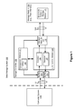
- FIG. 1 is a diagram of an implementation of a data storage system 100 , in accordance with some embodiments. While some example features are illustrated, various other features have not been illustrated for the sake of brevity and so as not to obscure more pertinent aspects of the example embodiments disclosed herein. To that end, as a non-limiting example, data storage system 100 includes a storage controller 120 , and a storage medium 130 , and is used in conjunction with a computer system 110 .
- storage medium 130 is a single flash memory device while in other embodiments storage medium 130 includes a plurality of flash memory devices.
- storage medium 130 is NAND-type flash memory or NOR-type flash memory.
- storage controller 120 is a solid-state drive (SSD) controller.
- a flash memory device includes one or more flash memory die, one or more flash memory packages, one or more flash memory channels, one or more SSDs, one or more SSD arrays, or the like.
- Computer system 110 is coupled to storage controller 120 through data connections 101 .
- computer system 110 includes storage controller 120 as a component and/or a sub-system.
- storage controller 120 may be any suitable computer device, such as a computer, a laptop computer, a tablet device, a netbook, an internet kiosk, a personal digital assistant, a mobile phone, a smart phone, a gaming device, a computer server, or any other computing device.
- Computer system 110 is sometimes called a host or host system.
- computer system 110 includes one or more processors, one or more types of memory, a display and/or other user interface components such as a keyboard, a touch screen display, a mouse, a track-pad, a digital camera and/or any number of supplemental devices to add functionality.
- processors one or more types of memory
- display and/or other user interface components such as a keyboard, a touch screen display, a mouse, a track-pad, a digital camera and/or any number of supplemental devices to add functionality.
- Storage medium 130 is coupled to storage controller 120 through connections 103 .
- Connections 103 are sometimes called data connections, but typically convey commands in addition to data, and optionally convey metadata, error correction information and/or other information in addition to data values to be stored in storage medium 130 and data values read from storage medium 130 .
- storage controller 120 and storage medium 130 are included in the same device as components thereof.
- memory controller 120 and storage medium 130 are embedded in a host device, such as a mobile device, tablet, other computer or computer controlled device, and the methods described herein are performed by the embedded memory controller.
- Storage medium 130 may include any number (i.e., one or more) of memory devices including, without limitation, non-volatile semiconductor memory devices, such as flash memory.
- flash memory devices can be configured for enterprise storage suitable for applications such as cloud computing, for database applications, primary and/or secondary storage, or for caching data stored (or to be stored) in secondary storage, such as hard disk drives. Additionally and/or alternatively, flash memory can also be configured for relatively smaller-scale applications such as personal flash drives or hard-disk replacements for personal, laptop, and tablet computers.
- Storage medium 130 is divided into a number of addressable and individually selectable blocks, such as selectable portion 131 .
- the individually selectable blocks are the minimum size erasable units in a flash memory device.
- each block contains the minimum number of memory cells that can be erased simultaneously.
- Each block is usually further divided into a plurality of pages and/or word lines, where each page or word line is typically an instance of the smallest individually accessible (readable) portion in a block.
- the smallest individually accessible unit of a data set is a sector, which is a subunit of a page. That is, a block includes a plurality of pages, each page contains a plurality of sectors, and each sector is the minimum unit of data for reading data from the flash memory device.
- one block comprises any number of pages, for example, 64 pages, 128 pages, 256 pages or another suitable number of pages.
- Blocks are typically grouped into a plurality of zones. Each block zone can be independently managed to some extent, which increases the degree of parallelism for parallel operations and simplifies management of storage medium 130 .
- error control coding can be utilized to limit the number of uncorrectable errors that are introduced by electrical fluctuations, defects in the storage medium, operating conditions, device history, write-read circuitry, etc., or a combination of these and various other factors.
- storage controller 120 includes a management module 121 , an input buffer 123 , an output buffer 124 , an error control module 125 and a storage medium interface (I/O) 128 .
- Storage controller 120 may include various additional features that have not been illustrated for the sake of brevity and so as not to obscure more pertinent features of the example embodiments disclosed herein, and that a different arrangement of features may be possible.
- Input and output buffers 123 , 124 provide an interface to computer system 110 through data connections 101 .
- storage medium I/O 128 provides an interface to storage medium 130 though connections 103 .
- storage medium I/O 128 includes read and write circuitry, including circuitry capable of providing reading signals to storage medium 130 (e.g., reading threshold voltages for NAND-type flash memory).
- management module 121 includes one or more processing units (CPUs, also sometimes called processors) 122 configured to execute instructions in one or more programs (e.g., in management module 121 ). In some embodiments, one or more CPUs 122 are shared by one or more components within, and in some cases, beyond the function of storage controller 120 . Management module 121 is coupled to input buffer 123 , output buffer 124 (connection not shown), error control module 125 and storage medium I/O 128 in order to coordinate the operation of these components.
- CPUs also sometimes called processors
- Error control module 125 is coupled to storage medium I/O 128 , input buffer 123 and output buffer 124 . Error control module 125 is provided to limit the number of uncorrectable errors inadvertently introduced into data. In some embodiments, error control module 125 is executed in software by the one or more CPUs 122 of management module 121 , and, in other embodiments, error control module 125 is implemented in whole or in part using special purpose circuitry to perform encoding and decoding functions. In some embodiments, error control module 125 is implemented in whole or in part by software executed on computer system 110 . To that end, error control module 125 includes an encoder 126 and a decoder 127 . Encoder 126 encodes data by applying an error control code to produce a codeword, which is subsequently stored in storage medium 130 .
- decoder 127 applies a decoding process to the encoded data to recover the data, and to correct errors in the recovered data within the error correcting capability of the error control code.
- error control codes have different error detection and correction capacities, and that particular codes are selected for various applications for reasons beyond the scope of this disclosure. As such, an exhaustive review of the various types of error control codes is not provided herein.
- each type or family of error control codes may have encoding and decoding algorithms that are particular to the type or family of error control codes.
- input buffer 123 receives data to be stored in storage medium 130 from computer system 110 .
- the data held in input buffer 123 is made available to encoder 126 , which encodes the data to produce one or more codewords.
- the one or more codewords are made available to storage medium I/O 128 , which transfers the one or more codewords to storage medium 130 in a manner dependent on the type of storage medium being utilized.
- a read operation is initiated when computer system (host) 110 sends one or more host read commands (e.g., via data connections 101 ) to storage controller 120 requesting data from storage medium 130 .
- Storage controller 120 sends one or more read access commands to storage medium 130 , via storage medium I/O 128 , to obtain raw read data in accordance with memory locations (addresses) specified by the one or more host read commands.
- Storage medium I/O 128 provides the raw read data (e.g., comprising one or more codewords) to decoder 127 . If the decoding is successful, the decoded data is provided to output buffer 124 , where the decoded data is made available to computer system 110 . In some embodiments, if the decoding is not successful, storage controller 120 may resort to a number of remedial actions or provide an indication of an irresolvable error condition.
- Flash memory devices utilize memory cells to store data as electrical values, such as electrical charges or voltages.
- Each flash memory cell typically includes a single transistor with a floating gate that is used to store a charge, which modifies the threshold voltage of the transistor (i.e., the voltage needed to turn the transistor on).
- the magnitude of the charge, and the corresponding threshold voltage the charge creates, is used to represent one or more data values.
- a reading threshold voltage is applied to the control gate of the transistor and the resulting sensed current or voltage is mapped to a data value.
- cell voltage and “memory cell voltage,” in the context of flash memory cells, means the threshold voltage of the memory cell, which is the minimum voltage that needs to be applied to the gate of the memory cell's transistor in order for the transistor to conduct current.
- reading threshold voltages sometimes also called reading signals and reading voltages
- gate voltages applied to the gates of the flash memory cells to determine whether the memory cells conduct current at that gate voltage.
- the raw data value for that read operation is a “1” and otherwise the raw data value is a “0.”
- FIG. 2A is a block diagram illustrating an exemplary management module 121 in accordance with some embodiments.
- Management module 121 typically includes: one or more processing units (CPUs) 122 for executing modules, programs and/or instructions stored in memory 202 and thereby performing processing operations; memory 202 ; and one or more communication buses 204 for interconnecting these components.
- One or more communication buses 204 optionally, include circuitry (sometimes called a chipset) that interconnects and controls communications between system components.
- Management module 121 is coupled to buffer 123 , buffer 124 , error control module 125 , and storage medium I/O 128 by one or more communication buses 204 .
- Memory 202 includes high-speed random access memory, such as DRAM, SRAM, DDR RAM or other random access solid state memory devices, and may include non-volatile memory, such as one or more magnetic disk storage devices, optical disk storage devices, flash memory devices, or other non-volatile solid state storage devices.
- Memory 202 optionally, includes one or more storage devices remotely located from the CPU(s) 122 .
- Memory 202 or alternatively the non-volatile memory device(s) within memory 202 , comprises a non-transitory computer readable storage medium.
- Each of the above identified elements may be stored in one or more of the previously mentioned memory devices, and corresponds to a set of instructions for performing a function described above.
- the above identified modules or programs i.e., sets of instructions
- memory 202 may store a subset of the modules and data structures identified above.
- memory 202 may store additional modules and data structures not described above.
- the programs, modules, and data structures stored in memory 202 , or the non-transitory computer readable storage medium of memory 202 provide instructions for implementing any of the methods described below with reference to FIGS. 8A-8C .
- some or all of these modules may be implemented with specialized hardware circuits that subsume part or all of the module functionality.
- FIG. 2A shows a management module 121
- FIG. 2A is intended more as functional description of the various features which may be present in a management module than as a structural schematic of the embodiments described herein.
- the programs, modules, and data structures shown separately could be combined and some programs, modules, and data structures could be separated.
- FIG. 2B is a block diagram illustrating an implementation of a characterization vector table 234 in accordance with some embodiments.
- Characterization vector table 234 includes a collection of characterization vectors 236 , that each store characterization data associated with a respective portion of a storage medium 130 (e.g., a distinct device, die, block zone, block, word line, word line zone or page portion of storage medium 130 ).
- each vector e.g., vector 236 - 1 , vector 236 - 2 , . . .
- vector 236 - n in the collection of characterization vectors 236 stores characterization data derived during each of at least two time periods (e.g., time T-1 and time T-2, or Xprogram-erase (PE) cycles and 2 ⁇ PE cycles).
- the characterization data stored in the characterization vectors 236 is statistically derived.
- a storage medium e.g., storage medium 130 , FIG. 1
- characterization vector table 234 includes at least one characterization vector for each distinct flash memory device.
- characterization vector table 234 includes a set of distinct characterization vectors 236 for each flash memory device in storage medium 130 , and the set of distinct characterization vectors 236 for each flash memory device includes at least one distinct characterization vector for each flash memory die in the flash memory device. More detailed example embodiments of characterization vectors 236 are described below with reference to FIG. 2C .
- FIG. 2C is a schematic diagram of an implementation of a characterization vector 240 (e.g., corresponding to one of characterization vectors 236 shown in FIG. 2B ) for a respective flash memory device of the plurality of flash memory devices in accordance with some embodiments.
- characterization data stored in characterization vector 240 for the respective flash memory device includes storage medium characterization parameter values such as a failed block counter field 242 indicating a number of failed flash memory blocks for the respective flash memory device, a program-erase (PE) cycles field 244 indicating a current count of the number of PE cycles performed on the respective flash memory device, and a reading threshold voltage field 246 with one or more reading threshold voltages for the respective flash memory device.
- PE program-erase
- the one or more storage medium characterization parameter values provide an indication of at least one of: a physical characteristic associated with the respective portion the storage medium (e.g., a distinct flash memory device, die, block zone, block, word line, word line zone or page portion of storage medium 130 ), a mode of operation associated with the respective portion of the storage medium, a history of use associated with the respective portion of the storage medium, a condition characteristic associated with the respective portion of the storage medium, a read type associated with the respective portion of the storage medium, and location(s) associated with the respective portion of the storage medium.
- a physical characteristic associated with the respective portion the storage medium e.g., a distinct flash memory device, die, block zone, block, word line, word line zone or page portion of storage medium 130
- a mode of operation associated with the respective portion of the storage medium
- a history of use associated with the respective portion of the storage medium
- a condition characteristic associated with the respective portion of the storage medium e.g., a read type associated with the respective portion of the storage medium
- FIG. 3A is a block diagram of a storage medium (e.g., an enterprise storage environment) divided into a plurality of logical chunks in accordance with some embodiments.
- FIG. 3A shows storage medium 130 comprising a plurality of flash memory devices (e.g., devices 1, 2, 3, 4, 5, 6, . . . ).
- storage medium 130 comprises a greater or lesser number of flash memory devices.
- each of the plurality of flash memory devices is a single die or a multi-die flash memory device.
- storage controller 120 and storage medium 130 comprise a storage system, where storage medium 130 comprises one or more memory devices such as flash memory devices.
- storage controller 120 or a component thereof is configured to divide the flash memory devices into a plurality of logical chunks.
- device 1 is divided into logical chunks 1a, 1b, 1c, 1d, 1e, 1f.
- Each logical chunk is assigned to a logical address (or set of logical addresses) which is mapped to a physical address (or set of physical addresses) in logical to physical mapping 220 .
- logical chunk 1a is mapped to a first range of physical addresses at device 1.
- storage controller 120 or a component thereof is configured to maintain and update logical to physical mapping 220 as a logical chunk migrates from a first flash memory device to a second flash memory device.
- storage medium 130 includes origin devices 1, 2, 3, 4 and spare devices 5, 6.
- the origin devices are flash memory devices that initially store data
- the spare devices are reserve flash memory devices that store replicated data originating from one of the origin devices.
- data is stored in the logical chunks of origin devices 1-4.
- FIG. 3A illustrates storage medium 130 including four origin devices and two spare devices; however, as will be understood by one of skill in the art, storage medium 130 may include any number of origin and spare devices and that the devices are not necessarily all the same size.
- storage controller 120 or a component thereof is configured to arrange the plurality of logical chunks into redundancy sets, where each redundancy set includes one or more logical chunks.
- each redundancy set stores redundant data sufficient to enable recovery of data stored in at least one of the one or more logical chunks.
- representative redundancy set 310 includes logical chunks 1a, 2a, 3a, 4a.
- representative redundancy set 310 is redundantly encoded across the four origin devices (e.g., a contiguous RAID stripe).
- representative redundancy set 320 includes logical chunks 1e, 2e, 3e, 4e and is arranged with a similar organizational scheme as representative redundancy set 310 .
- FIG. 3B is a block diagram of a storage medium divided into a plurality of logical chunks in accordance with some embodiments.
- storage controller 120 or a component thereof e.g., selection module 226 , FIG. 2A
- selection module 226 FIG. 2A
- FIGS. 5-7 the migration process is discussed in more detail below with respect to method 800 .
- the migration process includes replicating the selected logical chunk and storing the replicated logical chunk, comprising a copy of the selected logical chunk, at a spare device.
- storage controller 120 or a component thereof notifies the origin device that the selected logical chunk is now free (e.g., via a TRIM or UNMAP command for a standard SSD).
- the replicated logical chunk is stored at the spare device in accordance with a preferred storage utilization scheme.
- the preferred storage utilization scheme requires that the replicated logical chunk, which is assigned to a same redundancy set as the selected logical chunk, be stored in a spare device that does not include any logical chunks in the redundancy set and/or that the replicated logical chunk be stored at a location in the spare device such that the replicated logical chunk is stored in a same contiguous stripe as the other logical chunks in the redundancy set.
- storage controller 120 or a component thereof detects a first predefined trigger condition in storage medium 130 corresponding to origin device 1.
- storage controller 120 or a component thereof e.g., selection module 226 , FIG. 2A
- selects logical chunk 1a e.g., shown as crossed out
- representative redundancy set 310 for migration after detecting the predefined trigger condition as to origin device 1.
- storage controller 120 or a component thereof e.g., storing module 228 , FIG.
- replicated logical chunk 1a comprises a copy of logical chunk 1a, at a spare device (e.g., spare device 5) that does not store any of the logical chunks in representative redundancy set 310 .
- a spare device e.g., spare device 5
- replicated logical chunk 1a is stored at a location in spare device 5 such that replicated logical chunk 1a is stored in a same contiguous stripe as the other logical chunks in representative redundancy set 310 (e.g., the first location (or the first range of physical addresses) at spare device 5).
- the condition triggering the migration does not have to originate within the logical chunk that is selected for migration, just within the same device.
- FIG. 3C is a block diagram of a storage medium divided into a plurality of logical chunks in accordance with some embodiments.
- storage controller 120 or a component thereof detects a second predefined trigger condition in storage medium 130 corresponding to origin device 3.
- storage controller 120 or a component thereof e.g., selection module 226 , FIG. 2A
- selects logical chunk 3a e.g., shown as crossed out
- representative redundancy set 310 for migration after detecting the predefined trigger condition as to origin device 3.
- FIG. 3C is a block diagram of a storage medium divided into a plurality of logical chunks in accordance with some embodiments.
- storage controller 120 or a component thereof detects a second predefined trigger condition in storage medium 130 corresponding to origin device 3.
- storage controller 120 or a component thereof selects logical chunk 3a (e.g., shown as crossed out) in representative redundancy set 310 for migration after detecting the predefined trigger condition as to origin device 3.
- logical chunk 3a
- 3C for example, storage controller 120 or a component thereof (e.g., storing module 228 , FIG. 2A ) stores replicated logical chunk 3a, comprising a copy of logical chunk 3a, at a spare device (e.g., spare device 6) that does not store any of the logical chunks in representative redundancy set 310 .
- replicated logical chunk 3a is stored at a location in spare device 6 such that replicated logical chunk 3a is stored in a same contiguous stripe as the other logical chunks in representative redundancy set 310 (e.g., the first location (or the first range of physical addresses) at spare device 6).
- storage controller 120 or a component thereof detects a third predefined trigger condition in storage medium 130 corresponding to origin device 2.
- storage controller 120 or a component thereof e.g., selection module 226 , FIG. 2A
- selects logical chunk 2e e.g., shown as crossed out
- representative redundancy set 320 for migration after detecting the predefined trigger condition as to origin device 2.
- storage controller 120 or a component thereof e.g., storing module 228 , FIG.
- replicated logical chunk 2e stores replicated logical chunk 2e, comprising a copy of logical chunk 2e, at a spare device (e.g., spare device 5) that does not store any of the logical chunks in representative redundancy set 320 .
- a spare device e.g., spare device 5
- replicated logical chunk 2e is stored at a location in spare device 5 such that replicated logical chunk 2e is stored in a same contiguous stripe as the other logical chunks in representative redundancy set 320 (e.g., the fifth location (or the fifth range of physical addresses) at spare device 5).
- FIG. 4A is a block diagram of a storage medium (e.g., an enterprise storage environment) divided into a plurality of logical chunks in accordance with some embodiments.
- FIG. 4A shows storage medium 130 comprising a plurality of flash memory devices (e.g., devices 1, 2, 3, 4, 5, 6, . . . ).
- storage medium 130 comprises a greater or lesser number of flash memory devices.
- each of the plurality of flash memory devices is a single die or a multi-die flash memory device.
- storage controller 120 and storage medium 130 comprise a storage system.
- storage controller 120 or a component thereof is configured to divide the flash memory devices into a plurality of logical chunks.
- device 1 is divided into logical chunks 1a, 1b, 1c, 1d, 1e, 1f.
- Each logical chunk is assigned to a logical address (or set of logical addresses) which is mapped to a physical address (or set of physical addresses) in logical to physical mapping 220 .
- logical chunk 1a is mapped to a first location (or first range of physical addresses) at device 1.
- management storage controller 120 or a component thereof is configured to maintain and update logical to physical mapping 220 as a logical chunk migrates from a first flash memory device to a second flash memory device.
- storage medium 130 includes origin devices 1, 2, 3, 4 and spare devices 5, 6.
- the origin devices are flash memory devices that initially store data
- the spare devices are reserve flash memory devices that store replicated data originating from one of the origin devices.
- data is stored in the logical chunks of origin devices 1-4.
- FIG. 4A illustrates storage medium 130 including four origin devices and two spare devices; however, as will be understood by one of skill in the art, storage medium 130 may include any number of origin and spare devices.
- FIG. 4B is a diagram of an indirection table corresponding to the plurality of logical chunks in FIG. 4A in accordance with some embodiments.
- storage controller 120 or a component thereof e.g., redundancy module 214 , FIG. 2A
- redundancy module 214 FIG. 2A
- each redundancy set stores redundant data sufficient to enable recovery of data stored in at least one of the one or more logical chunks.
- Indirection table 216 contains the location (e.g., physical address) of the one or more logical chunks in each redundancy set.
- storage controller 120 or a component thereof e.g., redundancy module 214 , FIG. 2A
- redundancy module 214 FIG. 2A
- indirection table 216 is configured to maintain and update indirection table 216 as the physical addresses of the one or more logical chunks in the redundancy sets change over time (e.g., as a logical chunk migrates from a first flash memory device to a second flash memory device).
- indirection table 216 illustrates that the physical address for logical chunk 1 in redundancy set 1 is located in the first location (or first range of physical addresses) at origin device 1 (e.g., indicated by coordinates 1,1), the physical address for logical chunk 2 in redundancy set 1 is located in the first location (or first range of physical addresses) at origin device 2 (e.g., indicated by coordinates 2,1), the physical address for logical chunk 3 in redundancy set 1 is located in the first location (or first range of physical addresses) at origin device 3 (e.g., indicated by coordinates 3,1), and the physical address for logical chunk 4 in redundancy set 1 is located in the first location (or first range of physical addresses) at origin device 4 (e.g., indicated by coordinates 4,1).
- redundancy set 1 including logical chunks 1a, 2a, 3a, 4a is redundantly encoded across the four origin devices (e.g., a contiguous RAID stripe).
- redundancy sets 2-6 are arranged with a similar organizational scheme as redundancy set 1.
- redundancy sets 1 including logical chunks 1a, 2a, 3a, 4a is redundantly encoded across the four origin devices (e.g., a contiguous RAID stripe).
- redundancy sets 2-6 are arranged with a similar organizational scheme as redundancy set 1.
- redundancy schemes could be implemented but are not discussed here for sake of brevity.
- FIG. 4C is a block diagram of a storage medium divided into a plurality of logical chunks in accordance with some embodiments.
- storage controller 120 or a component thereof e.g., selection module 226 , FIG. 2A
- selection module 226 FIG. 2A
- FIGS. 5-7 the migration process is discussed in more detail below with respect to method 800 .
- the migration process includes replicating the selected logical chunk and storing the replicated logical chunk, comprising a copy of the selected logical chunk, at a spare device.
- storage controller 120 or a component thereof notifies the origin device that the selected logical chunk is now free (e.g., via a TRIM or UNMAP command for a standard SSD). It should be noted that the condition triggering the migration does not have to originate within the logical chunk that is selected for migration, just within the same device.
- the replicated logical chunk is stored at the spare device in accordance with a preferred storage utilization scheme.
- the preferred storage utilization scheme requires that the replicated logical chunk be stored at a first available location in a spare device.
- the preferred storage utilization scheme requires that the replicated logical chunk, which is assigned to a same redundancy set as the selected logical chunk, be stored at a first available location in a spare device that includes no logical chunks in the redundancy set.
- the preferred storage utilization scheme requires that the replicated logical chunk, which is assigned to a same redundancy set as the selected logical chunk, be stored in a spare device that does not include any logical chunks in the redundancy set and that the replicated logical chunk be stored at a first available location that is not in a same contiguous stripe as the other logical chunks in the redundancy set.
- storage controller 120 or a component thereof detects a first predefined trigger condition in storage medium 130 corresponding to origin device 3.
- storage controller 120 or a component thereof e.g., selection module 226 , FIG. 2A
- selects logical chunk 3c e.g., shown as crossed out
- redundancy set 3 for migration after detecting the predefined trigger condition as to origin device 3.
- storage controller 120 or a component thereof e.g., storing module 228 , FIG.
- replicated logical chunk 3c comprises a copy of logical chunk 3c, at spare device 5 because spare device 5 does not store any logical chunks in redundancy set 3.
- replicated logical chunk 3c is stored at a first available location in spare device 5 that is not in the same contiguous stripe as the other logical chunks in redundancy set 3 (e.g., in the first location (or the first range of physical addresses) at spare device 5 indicated by coordinates 5,1).
- storage controller 120 or a component thereof detects a second predefined trigger condition in storage medium 130 corresponding to origin device 4.
- storage controller 120 or a component thereof e.g., selection module 226 , FIG. 2A
- selects logical chunk 4b e.g., shown as crossed out
- redundancy set 2 for migration after detecting the predefined trigger condition as to origin device 4.
- storage controller 120 or a component thereof e.g., storing module 228 , FIG.
- replicated logical chunk 4b comprises a copy of logical chunk 4b, at spare device 5 because spare device 5 does not store any logical chunks in redundancy set 2.
- replicated logical chunk 4b is optionally stored at a first available location in spare device 5 that is not in the same failure domain as the other logical chunks in redundancy set 2 (e.g., in the third location (or the third range of physical addresses) at spare device 5 indicated by coordinates 5,3).
- storage controller 120 or a component thereof detects a third predefined trigger condition in storage medium 130 corresponding to origin device 1.
- storage controller 120 or a component thereof e.g., selection module 226 , FIG. 2A
- selects logical chunk 1d e.g., shown as crossed out
- redundancy set 4 for migration after detecting the predefined trigger condition as to origin device 1.
- storage controller 120 or a component thereof e.g., storing module 228 , FIG.
- replicated logical chunk 1d comprises a copy of logical chunk 1d, at spare device 5 because spare device 5 does not store any logical chunks in redundancy set 4.
- replicated logical chunk 1d is optionally stored at a first available location in spare device 5 that is not in the same contiguous stripe as the other logical chunks in redundancy set 4 (e.g., in the second location (or the second range of physical addresses) at spare device 5 indicated by coordinates 5,2).
- storage controller 120 or a component thereof detects a fourth predefined trigger condition in storage medium 130 corresponding to origin device 2.
- storage controller 120 or a component thereof e.g., selection module 226 , FIG. 2A
- selects logical chunk 2d e.g., shown as crossed out
- redundancy set 4 for migration after detecting the predefined trigger condition as to origin device 2.
- storage controller 120 or a component thereof e.g., storing module 228 , FIG.
- replicated logical chunk 2d comprises a copy of logical chunk 2d, at spare device 6 because spare device 6 does not store any logical chunks in redundancy set 4.
- replicated logical chunk 2d is stored at a first available location in spare device 6 that is not in the same contiguous stripe as the other logical chunks in redundancy set 4 (e.g., in the first location (or the first range of physical addresses) at spare device 6 indicated by coordinates 6,1).
- storage controller 120 or a component thereof detects a fifth predefined trigger condition in storage medium 130 corresponding to origin device 1.
- storage controller 120 or a component thereof e.g., selection module 226 , FIG. 2A
- selects logical chunk 1a e.g., shown as crossed out
- redundancy set 1 for migration after detecting the second predefined trigger condition as to origin device 1.
- storage controller 120 or a component thereof e.g., storing module 228 , FIG.
- replicated logical chunk 1a stores replicated logical chunk 1a, comprising a copy of logical chunk 1a, at spare device 5 because spare device 5 does not store any logical chunks in redundancy set 1.
- replicated logical chunk 1a is stored at a first available location in spare device 5 that is not in the same contiguous stripe as the other logical chunks in redundancy set 1 (e.g., in the fourth location (or the fourth range of physical addresses) at spare device 5 indicated by coordinates 5,4).
- FIG. 4D is a diagram of an indirection table corresponding to the plurality of logical chunks in FIG. 4C in accordance with some embodiments.
- indirection table 216 is an updated version of the indirection table illustrated in FIG. 4B .
- indirection table 216 reflects the new locations (or physical addresses) of the logical chunks that were migrated as described above with respect to FIG. 4C .
- logical chunks 1 and 2 in redundancy set 4 have new physical addresses (e.g., indicated by coordinates 5,2 and 6,1, respectively).
- logical chunk 1d has been migrated off of origin device 1 to the second location (or range of physical addresses) at spare device 5 (e.g., coordinates 5,2)
- logical chunk 2d has been migrated off of origin device 2 to the first location (or range of physical addresses) at spare device 6 (e.g., coordinates 6,1) in accordance with the preferred storage utilization scheme.
- logical chunk 1 in redundancy set 4 e.g., logical chunk 1d
- logical chunk 2 in redundancy set 4 e.g., logical chunk 2d
- location (2,4) to location (6,1).
- 4C-4D requires that the replicated logical chunk, which is assigned to a same redundancy set as the selected logical chunk, be stored in a spare device that does not include any logical chunks in the redundancy set and that the replicated logical chunk be stored at a first available location that is not in the same contiguous stripe as the other logical chunks in the redundancy set.
- the replicated chunk need not be in the same contiguous stripe as the other logical chunks in the redundancy set.
- FIG. 5 illustrates a flowchart representation of a method 500 of triggering a migration process in accordance with some embodiments.
- method 500 is performed at a storage system including storage controller 120 and a plurality of flash memory devices (e.g., storage medium 130 , FIG. 1 ) including a respective flash memory device.
- a storage system including storage controller 120 and a plurality of flash memory devices (e.g., storage medium 130 , FIG. 1 ) including a respective flash memory device.
- the respective flash memory device determines that a threshold number of flash memory blocks of the respective flash memory device have failed or will fail in the near future.
- each of the plurality of flash memory devices maintains a counter indicating a number of failed flash memory blocks for the respective flash memory device.
- storage controller 120 or a component thereof is configured to maintain a counter for each of the plurality of flash memory devices indicating a number of failed flash memory blocks for a respective flash memory device of the plurality of flash memory devices.
- storage controller 120 or a component thereof is configured to store and maintain a collection of characterization vectors 236 for each of the plurality of flash memory devices in a characterization vector table 234 .
- a respective characterization vector 236 for a respective flash memory device includes a failed block counter field 242 indicating a number of failed flash memory blocks for the respective flash memory device.
- a flash memory block fails when one or more codewords read from the flash memory block are uncorrectable or other ECC information produced after one or more codewords are read from the flash memory block indicates that a bit error rate corresponding to the one or more codewords exceeds a predefined threshold.
- a flash memory block fails when a count of PE cycles for the flash memory block exceeds a predefined threshold.
- the threshold number of failed flash memory blocks is equal to the number of flash memory blocks in a logical chunk. In some embodiments, the threshold number of failed flash memory blocks is equal to an integer multiple of the number of flash memory blocks in a logical chunk.
- the respective flash memory device reduces its advertised size.
- the difference between the current (or reduced) advertised size and the previous advertised size is equal to the number of flash memory blocks comprising a logical chunk.
- the advertised size of a flash memory device is an amount of bytes or addresses advertised to storage controller 120 that is equal to the amount of logical chunks that are storing data and are available for storing data.
- the advertised size of a flash memory device is equal to the difference between the total amount of flash memory blocks comprising the flash memory device and the number of failed flash memory blocks.
- storage controller 120 directs a memory access request (e.g., a read or write operation) to the respective flash memory device.
- a memory access request e.g., a read or write operation
- storage controller 120 directs the memory access request to the respective flash memory device in response to a request from the host to perform a memory access operation at a logical address corresponding to a memory location associated with the respective flash memory device.
- the respective flash memory device returns a deferred error to storage controller 120 in response to receiving the memory access request.
- the deferred error indicates that a threshold number of flash memory blocks of the respective flash memory device have failed.
- the deferred error could be a deferred SCSI error which is only returned (or reported) to storage controller 120 upon reception of the memory access request.
- storage controller 120 queries the respective flash memory device so as to determine its current advertised size.
- storage controller 120 or a component thereof e.g., trigger condition detection module 222 , FIG. 2A
- storage controller 120 initiates a migration process (discussed in more detail below with respect to method 800 ) as to the respective flash memory device.
- the respective flash memory device returns the current (i.e., reduced) advertised size in response to receiving the query from storage controller 120 .
- storage controller 120 determines whether the current advertised size returned by the respective flash memory device is smaller than a previous advertised size of the respective flash memory device. In some embodiments, storage controller 120 determines whether the current advertised size returned by the respective flash memory device is smaller than the amount of data stored by the respective flash memory device. For example, this indicates that at least an amount of data equal to the difference between the current advertised size and the amount of data stored by the respective flash memory device needs to be migrated to a second flash memory device different from the respective flash memory device.
- step 516 in accordance with a determination that the current advertised size of the respective flash memory device is smaller than a previous advertised size of the respective flash memory device, storage controller 120 initiates a migration process (discussed in more detail below with respect to method 800 ) as to the respective flash memory device.
- FIG. 6 illustrates a flowchart representation of a method 600 of triggering a migration process in accordance with some embodiments.
- method 600 is performed at a storage system including storage controller 120 and a plurality of flash memory devices (e.g., storage medium 130 , FIG. 1 ) including a respective flash memory device.
- a storage system including storage controller 120 and a plurality of flash memory devices (e.g., storage medium 130 , FIG. 1 ) including a respective flash memory device.
- the respective flash memory device determines that a threshold number of flash memory blocks of the respective flash memory device have failed or may fail sometime in the near future. See discussion above with respect to step 502 FIG. 5 for examples of criteria for determining whether a respective flash memory device has failed.
- the respective flash memory device returns a notification to storage controller 120 in response to the determination in step 602 .
- the notification indicates that a threshold number of flash memory blocks of the respective flash memory device have failed.
- SCSI small computer system interface
- storage controller 120 in response to receiving the notification from the respective flash memory device, storage controller 120 initiates a migration process (discussed in more detail below with respect to method 800 ) as to the respective flash memory device.
- storage controller 120 or a component thereof e.g., trigger condition detection module 222 , FIG. 2A
- storage controller 120 or a component thereof is configured to detect a predefined trigger condition as to the respective flash memory device in response to receiving the error.
- FIG. 7 illustrates a flowchart representation of a method 700 of triggering a migration process in accordance with some embodiments.
- method 700 is performed at storage controller 120 .
- storage controller 120 determines that a threshold number of flash memory blocks have failed or may fail sometime in the near future for a respective flash memory device of a plurality of flash memory devices. See discussion above with respect to step 502 FIG. 5 for examples of criteria for determining whether a respective flash memory device has failed.
- storage controller 120 in response to determining that a threshold number of flash memory blocks for the respective flash memory device have failed, storage controller 120 initiates a migration process (discussed in more detail below with respect to method 800 ) as to the respective flash memory device.
- storage controller 120 or a component thereof e.g., trigger condition detection module 222 , FIG. 2A
- storage controller 120 or a component thereof is configured to detect a predefined trigger condition as to the respective flash memory device in response to determining that a threshold number of flash memory blocks for the respective flash memory device have failed.
- FIGS. 8A-8C illustrate a flowchart representation of a method 800 of managing a storage system that comprises a storage controller and a plurality of flash memory devices each with a plurality of flash memory blocks.
- method 800 is performed by storage controller 120 in FIG. 1 , which is distinct from and coupled to storage medium 130 in FIG. 1 (e.g., comprising the plurality of flash memory devices) by one or more connections (e.g., connections 103 , FIG. 1 ).
- connections e.g., connections 103 , FIG. 1
- Optional operations are indicated by dashed lines (e.g., boxes with dashed-line borders).
- method 800 is performed by storage controller 120 or one or more components of storage controller 120 (e.g., management module 121 , FIGS. 1 and 2A ).
- method 800 is governed by instructions that are stored in a non-transitory computer readable storage medium and the instructions are executed by one or more processors of a device, such as one or more processing units (CPUs) 122 of management module 121 .
- method 800 is performed in whole or in part by computer system 110 .
- the storage controller divides ( 802 ) each of the plurality of flash memory devices into a plurality of logical chunks, where each logical chunk includes one or more flash memory blocks.
- storage controller 120 or a component thereof e.g., logical chunk management module 212 , FIG. 2A
- storage controller 120 or a component thereof is configured to divide each of the plurality of flash memory devices into a plurality of logical chunks.
- the logical address (or set of logical addresses) for each of the plurality of logical chunks are associated with a physical address (or set of physical addresses) in a logical to physical mapping 220 .
- storage controller 120 or a component thereof e.g., mapping module 218 , FIG. 2A
- a size of the plurality of logical chunks is predetermined ( 804 ) by software. For example, an administrator of the storage system is enabled to determine the size of a logical chunk. Typically, the size of a logical chunk is greater than or equal to 1 MB.
- a size of the plurality of logical chunks is determined ( 806 ) based on a protocol used by the storage system. For example, when the small computer system interface (SCSI) protocol is used for the storage system, a logical chunk could be a logical unit number (LUN).
- SCSI small computer system interface
- LUN logical unit number
- the SCSI protocol supports up to 64,000 LUNs in the storage system; however, some operating systems only support up to 16,000 LUNs. For example, an 8 TB storage system could be divided into 16,000 500 MB LUNs.
- the storage controller detects ( 808 ) a predefined trigger condition with respect to a respective flash memory device of the plurality of flash memory devices.
- storage controller 120 or a component thereof detects a predefined trigger condition as to a respective flash memory device in response to receiving a deferred trigger from the respective flash memory device.
- the respective flash memory device sends a deferred error to storage controller 120 after receiving a memory access request from storage controller 120 .
- storage controller 120 or a component thereof e.g., trigger condition detection module 222 , FIG.
- a predefined trigger condition as to a respective flash memory device upon receiving a notification from the respective flash memory device.
- the respective flash memory device sends a proactive error to storage controller 120 after determining that a threshold number of flash memory blocks of the respective flash memory device have failed.
- storage controller 120 or a component thereof e.g., trigger condition detection module 222 , FIG. 2A ) detects a predefined trigger condition as to a respective flash memory device after determining that a threshold number of blocks for the respective flash memory device have failed.
- the detected predefined trigger condition is ( 810 ) one of a set of a predefined trigger conditions.
- the set of predefined trigger conditions includes: storage controller 120 receiving a deferred error from a respective flash memory device; storage controller 120 receiving a proactive error from a respective flash memory device; and storage controller 120 determining that a threshold number of blocks for a respective flash memory device have failed. Where the deferred or proactive errors are received by storage controller 120 , each of the plurality of flash memory devices maintains a counter indicating a number of failed flash memory blocks for the respective flash memory device.
- storage controller 120 determines that a threshold number of blocks for a respective flash memory device have failed, storage controller 120 maintains a counter for each of the plurality of flash memory devices indicating a number of failed flash memory blocks for a respective flash memory device of the plurality of flash memory devices.
- the storage controller detects ( 812 ) the predefined trigger condition after directing a memory access request to the respective flash memory device.
- storage controller 120 or a component thereof e.g., trigger condition detection module 222 , FIG. 2A . detects a predefined trigger condition as to a respective flash memory device in response to receiving the deferred error and after directing a memory access request to the respective flash memory device at step 506 .
- the predefined trigger condition indicates ( 814 ) that a counter of failed flash memory blocks for the respective flash memory device exceeds an integer multiple of a threshold number, the threshold number comprising the number of flash memory blocks included in a logical chunk or an integer multiple of the number of flash memory blocks included in a logical chunk.
- storage controller 120 receives a deferred error from a respective flash memory device indicating that that a counter of failed flash memory blocks for the respective flash memory device exceeds an integer multiple of a threshold number.
- storage controller 120 receives a proactive error from a respective flash memory device indicating that that a counter of failed flash memory blocks for the respective flash memory device exceeds an integer multiple of a threshold number.
- storage controller 120 determines that a counter of failed flash memory blocks for a respective flash memory device exceeds an integer multiple of a threshold number. For example, if a logical chunk comprises 10 flash memory blocks, the threshold number is 10 or an integer multiple of 10 (e.g., 20, 30, 40, 50, etc.). For example, when the threshold number is 10, the predefined trigger condition indicates that the counter of failed flash memory blocks for the respective flash memory device exceeds 10 or an integer multiple of 10 (e.g., 20, 30, 40, 50, etc.).
- the storage controller in response to detecting ( 816 ) the predefined trigger condition, queries ( 818 ) the respective flash memory device to determine whether the size of the respective flash memory device is smaller than a previous size of the respective flash memory device, and the selecting and storing are performed in accordance with a determination that the query indicates that the size of the respective flash memory device is smaller than the previous size of the respective flash memory device.
- storage controller 120 or a component thereof e.g., trigger condition detection module 222 , FIG. 2A ) detects a predefined trigger condition as to the respective flash memory device upon receiving the deferred trigger from the respective memory device.
- trigger condition detection module 222 FIG. 2A
- storage controller 120 or a component thereof queries the respective flash memory device at step 510 in response to detecting the predefined trigger condition as to the respective flash memory device.
- FIG. 5 shows storage controller 120 or a component thereof initiates the migration process (including the selecting and storing) at step 516 upon determining that the current advertised size of the device is smaller than the previous advertised size of the device at step 514 .
- the storage controller selects ( 820 ) one of the plurality of logical chunks of the respective flash memory device for migration in accordance with predefined selection criteria.
- FIG. 3B for example, in response to detecting the predefined trigger condition as to origin device 1, storage controller 120 or a component thereof (e.g., selection module 226 , FIG. 2A ) selects logical chunk 1a for migration.
- FIG. 4C for example, in response to detecting the predefined trigger condition as to origin device 3, storage controller 120 or a component thereof (e.g., selection module 226 , FIG. 2A ) selects logical chunk 3c for migration.
- storage controller 120 or a component thereof selects logical chunks 1a and 3c pseudo-randomly or in accordance with predefined selection criteria.
- predefined selection criteria include ( 822 ) a least utilized logical chunk or least populated logical chunk of the respective flash memory device. For example, in response to detecting the predefined trigger condition as to a respective flash memory device, storage controller 120 or a component thereof (e.g., selection module 226 , FIG. 2A ) selects a least utilized (e.g., least operated on) or a least populated logical chunk of the respective flash memory device so as to reduce the time and resources needed for the migration process.
- a least utilized e.g., least operated on
- predefined selection criteria include ( 824 ) the logical chunk associated with a memory access request. For example, in response to detecting the predefined trigger condition as to a respective flash memory device, storage controller 120 or a component thereof (e.g., selection module 226 , FIG. 2A ) selects the logical chunk associated with a current or next memory access request (e.g., a read or write operation).
- a current or next memory access request e.g., a read or write operation
- predefined selection criteria include a logical chunk that is simple or efficient for storage controller 120 to fetch at that time. For example, while the storage controller 120 is doing other tasks unrelated to method 800 (e.g., garbage collection or error scrubbing) on a logical chunk said logical chunk is selected prior to or after completion of the unrelated task.
- unrelated to method 800 e.g., garbage collection or error scrubbing
- the storage controller stores ( 826 ) a replicated logical chunk, comprising a copy of the selected logical chunk, at a second flash memory device different from the respective flash memory device.
- storage controller 120 or a component thereof e.g., storing module 228 , FIG. 2A
- FIG. 4C for example, storage controller 120 or a component thereof (e.g., storing module 228 , FIG.
- the selected chunk is stored in a different type of memory media than it was previously stored. For example, the selected logical chunk is migrated from flash memory to HDD or vice versa.
- storage controller 120 or a component thereof performs a migration process including the selecting ( 820 ), the storing ( 826 ), and the remapping ( 832 ).
- migration of a selected logical chunk includes the storing ( 826 ) and the remapping ( 832 ).
- storage controller 120 or a component thereof notifies the origin device that the selected logical chunk is now free (e.g., via a TRIM or UNMAP command for a standard SSD).
- the second flash memory device is ( 828 ) in a different failure domain than the respective flash memory device.
- storage medium 130 comprises an enterprise storage environment.
- the enterprise storage environment is organized into a hierarchy including a plurality of rows, a plurality of cabinets per row, a plurality of shelves per cabinet, and a plurality of flash memory devices per shelf.
- each of the levels of the hierarchy i.e., row, cabinet, shelf, flash memory device
- storage controller 120 or a component thereof e.g., storing module 228 , FIG. 2A ) stores the replicated logical chunk in a different failure domain than the one including the respective flash memory device.
- At least a predefined number of failure domains must be crossed when storing the replicated logical chunk. For example, if the respective flash memory device is located in row 1, cabinet 2, shelf 3 and the replicated logical chunk must cross one failure domain, the replicated flash memory device is at least stored in different shelf in row 1, cabinet 2.
- the storage controller in response to detecting ( 816 ) the predefined trigger condition, re-encodes ( 830 ) data in at least one logical chunk of the respective flash memory device with a higher level of error correction protection than a prior encoding of the data in the at least one logical chunk of the respective flash memory device.
- storage controller 120 or a component thereof e.g., re-encoding module 230 , FIG. 2A ) is configured to re-encode the data in one of the plurality of logical chunks of the respective flash memory device after the predefined trigger condition as to the respective flash memory device is detected.
- more parity bits are included (i.e., the parity-to-data ratio is increased) for the respective logical chunk.
- a stronger ECC scheme is used for the respective logical chunk.
- the data stored in the respective logical chunk is re-encoded from Bose-Chaudhuri-Hocquenghem (BCH) encoding to low-density parity check (LDPC) encoding.
- BCH Bose-Chaudhuri-Hocquenghem
- LDPC low-density parity check
- the storage controller In response to detecting ( 816 ) the predefined trigger condition, the storage controller remaps ( 832 ) an address of the selected logical chunk to a physical location of the replicated logical chunk.
- storage controller 120 or a component thereof e.g., mapping module 218 , FIG. 2A
- mapping module 218 FIG. 2A
- storage controller 120 or a component thereof is configured to update logical to physical mapping 220 so that the physical address of the selected logical chunk (e.g., a location at the respective flash memory device) is replaced by the physical address of the replicated logical chunk (e.g., a location at a second device different from the respective flash memory device).
- mapping module 218 remaps the physical address associated with logical chunk 2e from the fifth location (or the fifth range of physical address) at origin device 2 to the fifth location (or the fifth range of physical address) at spare device 5 in logical to physical mapping 220 .
- the storage controller decreases ( 834 ) a number of logical chunks associated with the respective flash memory device.
- storage controller 120 or a component thereof e.g., logical chunk management module 212 , FIG. 2A
- storage controller 120 or a component thereof is configured to decrease a number of logical chunks associated with the respective flash memory device after migrating a selected logical chunk from the respective flash memory device to a second flash memory device different from the respective flash memory device.
- FIG. 3B for example, after detecting a predefined trigger condition as to origin device 1 and migrating logical chunk 1a to spare device 5, logical chunk management module 212 decreases the number of logical chunks associated with origin device 1 from six to five (e.g., indicated by crossing out logical chunk 1a).
- the logical chunks are allocated ( 836 ) for storing data and are organized into a plurality of redundancy sets, each redundancy set comprising one or more logical chunks and storing redundant data sufficient to enable recovery of data stored in at least one of the one or more logical chunks.
- data includes programs, instructions, ECC, metadata, user data, system data, and/or operator data.
- storage controller 120 or a component thereof e.g., redundancy module 214 , FIG. 2A
- redundancy module 214 FIG. 2A
- each redundancy set stores redundant data sufficient to enable recovery of data stored in at least one of the one or more logical chunks.
- representative redundancy set 310 including logical chunks 1a, 2a, 3a, 4a
- representative redundancy set 320 is redundantly encoded across the four origin devices (e.g., a contiguous RAID stripe).
- redundancy set 1 including logical chunks 1a, 2a, 3a, 4a
- redundancy set 1 is redundantly encoded across the four origin devices (e.g., a contiguous RAID stripe).
- the replicated logical chunk is included ( 838 ) in a respective redundancy set of the plurality of redundancy sets that formerly included the selected logical chunk. In some embodiments, the replicated chunk is included in the same contiguous stripe as the selected chunk. In FIG. 3B , for example, replicated logical chunk 1a is included in representative redundancy set 310 , which formerly included logical chunk 1a. In some embodiments, the replicated chunk is included in the same redundancy set via an indirection table. In FIGS. 4C-4D , for example, replicated logical chunk 4b (e.g., corresponding to coordinates 5,3) is included in redundancy set 2, which formerly included logical chunk 4b.
- replicated logical chunk 4b e.g., corresponding to coordinates 5,3
- a respective redundancy set of the plurality of redundancy sets is ( 840 ) a contiguous stripe across the plurality of flash memory devices, and the replicated logical chunk is stored in a same contiguous stripe as the selected logical chunk at the second flash memory device different from the respective flash memory device.
- the replicated logical chunk is assigned to the same redundancy set as the selected logical chunk.
- the replicated logical chunk is stored in a spare device that does not include other logical chunks in the redundancy set, and the replicated logical chunk is stored such that it is in the same contiguous stripe as the other logical chunks in the redundancy set.
- representative redundancy set 310 (including logical chunks 1a, 2a, 3a, 4a) is redundantly encoded across the four origin devices to form a contiguous stripe.
- replicated logical chunk 1a comprising a copy of logical chunk 1a, is stored at the first location (or first range of physical addresses) in spare device 5 such that it is in the contiguous stripe with the other logical chunks in representative redundancy set 310 (e.g., logical chunks 2a, 3a, 4a).
- the replicated logical chunk is stored ( 842 ) in accordance with a preferred storage utilization scheme, and the storage controller associates the replicated logical chunk with a respective redundancy set of the plurality of redundancy sets in an indirection table.
- the preferred storage utilization scheme illustrated in FIGS. 4C-4D requires that the replicated logical chunk, which is assigned to a same redundancy set as the selected logical chunk, be stored in a spare device that does not include any logical chunks in the redundancy set and that the replicated logical chunk be stored at a first available location that, optionally, is not in the same contiguous stripe as the other logical chunks in the redundancy set.
- replicad logical chunk 4b for example, storage controller 120 or a component thereof (e.g., storing module 228 , FIG. 2A ) stores replicated logical chunk 4b, comprising a copy of logical chunk 4b, at spare device 5 because spare device 5 does not store any logical chunks in redundancy set 2.
- replicated logical chunk 4b is stored at a first available location in spare device 5 that is not in the same contiguous stripe as the other logical chunks in redundancy set 2 (e.g., in the third location or the third range of physical addresses at spare device 5).
- storage controller 120 for example, storage controller 120 or a component thereof (e.g., redundancy module 214 ) updates indirection table 216 so that that logical chunk 4 in redundancy set 2 (e.g., logical chunk 4b) is remapped from location (4,2) to location (5,3).
- redundancy module 214 e.g., redundancy module 214
- first, second, etc. may be used herein to describe various elements, these elements should not be limited by these terms. These terms are only used to distinguish one element from another.
- a first flash memory device could be termed a second flash memory device, and, similarly, a second flash memory device could be termed a first flash memory device, which changing the meaning of the description, so long as all occurrences of the “first flash memory device” are renamed consistently and all occurrences of the “second flash memory device” are renamed consistently.
- the first flash memory device and the second flash memory device are both flash memory devices, but they are not the same flash memory device.
- the term “if” may be construed to mean “when” or “upon” or “in response to determining” or “in accordance with a determination” or “in response to detecting,” that a stated condition precedent is true, depending on the context.
- the phrase “if it is determined [that a stated condition precedent is true]” or “if [a stated condition precedent is true]” or “when [a stated condition precedent is true]” may be construed to mean “upon determining” or “in response to determining” or “in accordance with a determination” or “upon detecting” or “in response to detecting” that the stated condition precedent is true, depending on the context.
Abstract
Description
-
- a data read
module 206 for reading data fromstorage medium 130 comprising a plurality of flash memory devices; - a
data write module 208 for writing data tostorage medium 130; - a data erase
module 210 for erasing data fromstorage medium 130; - a logical
chunk management module 212 for dividing each of the plurality of flash memory devices into a plurality of logical chunks, including:- a redundancy module 214 for arranging the plurality of logical chunks into redundancy sets, including an indirection table 216 for maintaining the location (or physical address) of each logical chunk comprising a redundancy set;
- a
mapping module 218 for mapping a logical address (or a set of logical addresses) for each of the logical chunks to a physical address (or a set of physical addresses), including a logical to physical mapping 220 associating logical addresses with physical addresses for the plurality of logical chunks; - a trigger condition detection module 222 for detecting a trigger condition as to a respective flash memory device of the plurality of flash memory devices;
- a migration module 224 for performing a migration process, including:
- a
selection module 226 for selecting a logical chunk to be replicated; and - a
storing module 228 for storing a replicated logical chunk, comprising a copy of the selected logical chunk;
- a
- a re-encoding module 230 for re-encoding data in a logical chunk with a higher level of error correction protection; and
- a characterization vector table 234 that includes a collection of
characterization vectors 236 each storing characterization data for a respective portion of storage medium 130 (e.g., a flash memory device, die, block zone, block, word line, word line zone or page portion of storage medium 130).
- a data read
Claims (24)
Priority Applications (4)
Application Number | Priority Date | Filing Date | Title |
---|---|---|---|
US14/470,580 US9519577B2 (en) | 2013-09-03 | 2014-08-27 | Method and system for migrating data between flash memory devices |
PCT/US2014/053868 WO2015034901A1 (en) | 2013-09-03 | 2014-09-03 | Method and system for migrating data between flash memory devices |
CN201480056332.XA CN105637490B (en) | 2013-09-03 | 2014-09-03 | Method and system for the migrating data between flash memory device |
PCT/US2014/053941 WO2015034954A1 (en) | 2013-09-03 | 2014-09-03 | Process and apparatus to reduce declared capacity of a storage device by reducing a range of logical addresses |
Applications Claiming Priority (2)
Application Number | Priority Date | Filing Date | Title |
---|---|---|---|
US201361873324P | 2013-09-03 | 2013-09-03 | |
US14/470,580 US9519577B2 (en) | 2013-09-03 | 2014-08-27 | Method and system for migrating data between flash memory devices |
Publications (2)
Publication Number | Publication Date |
---|---|
US20150067244A1 US20150067244A1 (en) | 2015-03-05 |
US9519577B2 true US9519577B2 (en) | 2016-12-13 |
Family
ID=52584898
Family Applications (1)
Application Number | Title | Priority Date | Filing Date |
---|---|---|---|
US14/470,580 Active US9519577B2 (en) | 2013-09-03 | 2014-08-27 | Method and system for migrating data between flash memory devices |
Country Status (3)
Country | Link |
---|---|
US (1) | US9519577B2 (en) |
CN (1) | CN105637490B (en) |
WO (1) | WO2015034901A1 (en) |
Cited By (4)
Publication number | Priority date | Publication date | Assignee | Title |
---|---|---|---|---|
US20160124820A1 (en) * | 2014-11-03 | 2016-05-05 | Silicon Motion, Inc. | Data Storage Device and Flash Memory Control Method |
US11194711B2 (en) | 2019-08-02 | 2021-12-07 | Samsung Electronics Co., Ltd. | Storage device |
US11500583B2 (en) | 2019-08-02 | 2022-11-15 | Samsung Electronics Co., Ltd. | Storage device, an operation method of a storage system including the storage device in which data stored in apinned buffer area and a non-pinned buffer area is flushed according to a flush request/policy, and a host device controlling the storage device |
US11556464B2 (en) | 2019-08-02 | 2023-01-17 | Samsung Electronics Co., Ltd. | Storage device and operating method thereof |
Families Citing this family (19)
Publication number | Priority date | Publication date | Assignee | Title |
---|---|---|---|---|
US9367243B1 (en) | 2014-06-04 | 2016-06-14 | Pure Storage, Inc. | Scalable non-uniform storage sizes |
US9082512B1 (en) * | 2014-08-07 | 2015-07-14 | Pure Storage, Inc. | Die-level monitoring in a storage cluster |
US10324636B2 (en) * | 2016-08-25 | 2019-06-18 | Gm Global Technology Operations Llc. | Fail-operational system design pattern based on software code migration |
KR20180062246A (en) | 2016-11-30 | 2018-06-08 | 삼성전자주식회사 | Memory System |
US10379948B2 (en) * | 2017-10-02 | 2019-08-13 | Western Digital Technologies, Inc. | Redundancy coding stripe based on internal addresses of storage devices |
US10474528B2 (en) | 2017-10-02 | 2019-11-12 | Western Digital Technologies, Inc. | Redundancy coding stripe based on coordinated internal address scheme across multiple devices |
CN107704212B (en) * | 2017-10-31 | 2019-09-06 | 新华三信息技术有限公司 | A kind of data processing method and device |
CN109726033B (en) * | 2017-10-31 | 2022-05-06 | 伊姆西Ip控股有限责任公司 | Method, data storage system and computer readable medium for providing RAID data protection |
US10725941B2 (en) | 2018-06-30 | 2020-07-28 | Western Digital Technologies, Inc. | Multi-device storage system with hosted services on peer storage devices |
US10409511B1 (en) | 2018-06-30 | 2019-09-10 | Western Digital Technologies, Inc. | Multi-device storage system with distributed read/write processing |
CN110688323B (en) * | 2018-07-06 | 2023-11-17 | 华为技术有限公司 | System controller and system garbage recycling method |
WO2020007030A1 (en) | 2018-07-06 | 2020-01-09 | 华为技术有限公司 | System controller and system garbage recovery method |
JP7042716B2 (en) * | 2018-07-26 | 2022-03-28 | キオクシア株式会社 | Storage device and storage control method |
US10649843B2 (en) | 2018-08-03 | 2020-05-12 | Western Digital Technologies, Inc. | Storage systems with peer data scrub |
US10831603B2 (en) | 2018-08-03 | 2020-11-10 | Western Digital Technologies, Inc. | Rebuild assist using failed storage device |
US10901848B2 (en) * | 2018-08-03 | 2021-01-26 | Western Digital Technologies, Inc. | Storage systems with peer data recovery |
US10824526B2 (en) | 2018-08-03 | 2020-11-03 | Western Digital Technologies, Inc. | Using failed storage device in peer-to-peer storage system to perform storage-centric task |
US10592144B2 (en) | 2018-08-03 | 2020-03-17 | Western Digital Technologies, Inc. | Storage system fabric with multichannel compute complex |
US11182258B2 (en) | 2019-01-04 | 2021-11-23 | Western Digital Technologies, Inc. | Data rebuild using dynamic peer work allocation |
Citations (243)
Publication number | Priority date | Publication date | Assignee | Title |
---|---|---|---|---|
US4916652A (en) | 1987-09-30 | 1990-04-10 | International Business Machines Corporation | Dynamic multiple instruction stream multiple data multiple pipeline apparatus for floating-point single instruction stream single data architectures |
US5270979A (en) | 1991-03-15 | 1993-12-14 | Sundisk Corporation | Method for optimum erasing of EEPROM |
US5519847A (en) | 1993-06-30 | 1996-05-21 | Intel Corporation | Method of pipelining sequential writes in a flash memory |
US5530705A (en) | 1995-02-08 | 1996-06-25 | International Business Machines Corporation | Soft error recovery system and method |
US5537555A (en) | 1993-03-22 | 1996-07-16 | Compaq Computer Corporation | Fully pipelined and highly concurrent memory controller |
US5551003A (en) | 1992-12-11 | 1996-08-27 | International Business Machines Corporation | System for managing log structured array (LSA) of DASDS by managing segment space availability and reclaiming regions of segments using garbage collection procedure |
US5657332A (en) | 1992-05-20 | 1997-08-12 | Sandisk Corporation | Soft errors handling in EEPROM devices |
US5666114A (en) | 1994-11-22 | 1997-09-09 | International Business Machines Corporation | Method and means for managing linear mapped address spaces storing compressed data at the storage subsystem control unit or device level |
US5708849A (en) | 1994-01-26 | 1998-01-13 | Intel Corporation | Implementing scatter/gather operations in a direct memory access device on a personal computer |
US5943692A (en) | 1997-04-30 | 1999-08-24 | International Business Machines Corporation | Mobile client computer system with flash memory management utilizing a virtual address map and variable length data |
US5953255A (en) | 1997-12-24 | 1999-09-14 | Aplus Flash Technology, Inc. | Low voltage, low current hot-hole injection erase and hot-electron programmable flash memory with enhanced endurance |
US5982664A (en) | 1997-10-22 | 1999-11-09 | Oki Electric Industry Co., Ltd. | Semiconductor memory capable of writing and reading data |
US6000006A (en) | 1997-08-25 | 1999-12-07 | Bit Microsystems, Inc. | Unified re-map and cache-index table with dual write-counters for wear-leveling of non-volatile flash RAM mass storage |
US6016560A (en) | 1995-06-14 | 2000-01-18 | Hitachi, Ltd. | Semiconductor memory, memory device, and memory card |
US6018304A (en) | 1997-12-18 | 2000-01-25 | Texas Instruments Incorporated | Method and apparatus for high-rate n/n+1 low-complexity modulation codes with adjustable codeword length and error control capability |
US6070074A (en) | 1998-04-24 | 2000-05-30 | Trw Inc. | Method for enhancing the performance of a regenerative satellite communications system |
US6138261A (en) | 1998-04-29 | 2000-10-24 | Trw Inc. | Concatenated coding system for satellite communications |
US6182264B1 (en) | 1998-05-22 | 2001-01-30 | Vlsi Technology, Inc. | Smart dynamic selection of error correction methods for DECT based data services |
US6192092B1 (en) | 1998-06-15 | 2001-02-20 | Intel Corp. | Method and apparatus for clock skew compensation |
US6295592B1 (en) | 1998-07-31 | 2001-09-25 | Micron Technology, Inc. | Method of processing memory requests in a pipelined memory controller |
US6311263B1 (en) | 1994-09-23 | 2001-10-30 | Cambridge Silicon Radio Limited | Data processing circuits and interfaces |
US20020024846A1 (en) | 1996-09-30 | 2002-02-28 | Takayuki Kawahara | Semiconductor integrated circuit and data processing system |
US20020083299A1 (en) | 2000-12-22 | 2002-06-27 | International Business Machines Corporation | High speed remote storage controller |
US6442076B1 (en) | 2000-06-30 | 2002-08-27 | Micron Technology, Inc. | Flash memory with multiple status reading capability |
US6449625B1 (en) | 1999-04-20 | 2002-09-10 | Lucent Technologies Inc. | Use of a two-way stack approach to optimize flash memory management for embedded database systems |
JP2002532806A (en) | 1998-12-18 | 2002-10-02 | ユニシス コーポレーション | Computer system and method for operating multiple operating systems in different partitions of a computer system so that different partitions can communicate with each other via shared memory |
US20020152305A1 (en) | 2000-03-03 | 2002-10-17 | Jackson Gregory J. | Systems and methods for resource utilization analysis in information management environments |
US20020162075A1 (en) | 2001-04-30 | 2002-10-31 | Talagala Nisha D. | Storage array employing scrubbing operations at the disk-controller level |
US20020165896A1 (en) | 2001-05-02 | 2002-11-07 | Kim Jason Seung-Min | Multiprocessor communication system and method |
US6484224B1 (en) | 1999-11-29 | 2002-11-19 | Cisco Technology Inc. | Multi-interface symmetric multiprocessor |
US6516437B1 (en) | 2000-03-07 | 2003-02-04 | General Electric Company | Turbo decoder control for use with a programmable interleaver, variable block length, and multiple code rates |
US20030041299A1 (en) | 2001-08-23 | 2003-02-27 | Fujitsu Limited | Memory controller for multilevel cell memory |
US20030043829A1 (en) | 2001-07-06 | 2003-03-06 | Abbas Rashid | Cross-bar switch employing a multiple entry point FIFO |
US20030051090A1 (en) | 2001-09-10 | 2003-03-13 | Bonnett William B. | Apparatus and method for secure program upgrade |
US20030088805A1 (en) | 2001-09-28 | 2003-05-08 | Tim Majni | Error indication in a raid memory system |
US20030093628A1 (en) | 2001-11-14 | 2003-05-15 | Matter Eugene P. | Memory adaptedt to provide dedicated and or shared memory to multiple processors and method therefor |
US20030188045A1 (en) | 2000-04-13 | 2003-10-02 | Jacobson Michael B. | System and method for distributing storage controller tasks |
US20030189856A1 (en) | 2002-04-04 | 2003-10-09 | Samsung Electronics Co., Ltd. | Multi-level flash memory with temperature compensation |
US20030198100A1 (en) | 2001-12-04 | 2003-10-23 | Hitachi, Ltd. | Method of controlling the operation of non-volatile semiconductor memory chips |
US20030212719A1 (en) | 2002-05-08 | 2003-11-13 | Hitachi, Ltd. | Method for heap memory management and computer system using the same method |
US6678788B1 (en) | 2000-05-26 | 2004-01-13 | Emc Corporation | Data type and topological data categorization and ordering for a mass storage system |
US20040024957A1 (en) | 2001-08-07 | 2004-02-05 | Chun-Hung Lin | Window-based flash memory storage system and management and access methods thereof |
US20040024963A1 (en) | 2002-08-05 | 2004-02-05 | Nisha Talagala | Method and system for striping data to accommodate integrity metadata |
US20040073829A1 (en) | 1998-07-16 | 2004-04-15 | Olarig Sompong P. | Fail-over of multiple memory blocks in multiple memory modules in computer system |
US6757768B1 (en) | 2001-05-17 | 2004-06-29 | Cisco Technology, Inc. | Apparatus and technique for maintaining order among requests issued over an external bus of an intermediate network node |
US20040153902A1 (en) | 2003-01-21 | 2004-08-05 | Nexflash Technologies, Inc. | Serial flash integrated circuit having error detection and correction |
US6775792B2 (en) | 2001-01-29 | 2004-08-10 | Snap Appliance, Inc. | Discrete mapping of parity blocks |
US20040181734A1 (en) | 2003-03-14 | 2004-09-16 | Saliba George A. | Extended error correction codes |
EP1465203A1 (en) | 2003-04-03 | 2004-10-06 | Samsung Electronics Co., Ltd. | Nonvolatile memory with page copy capability and method thereof |
US20040199714A1 (en) | 1995-07-31 | 2004-10-07 | Petro Estakhri | Increasing the memory performance of flash memory devices by writing sectors simultaneously to multiple flash memory devices |
US6810440B2 (en) | 1999-06-09 | 2004-10-26 | Qlogic Corporation | Method and apparatus for automatically transferring I/O blocks between a host system and a host adapter |
US20040237018A1 (en) | 2003-05-23 | 2004-11-25 | Riley Dwight D. | Dual decode scheme |
US6836815B1 (en) | 2001-07-11 | 2004-12-28 | Pasternak Solutions Llc | Layered crossbar for interconnection of multiple processors and shared memories |
US6836808B2 (en) | 2002-02-25 | 2004-12-28 | International Business Machines Corporation | Pipelined packet processing |
US6842436B2 (en) | 1999-12-17 | 2005-01-11 | Siemens Aktiengesellschaft | Multiport-RAM memory device |
US20050060501A1 (en) | 2003-09-16 | 2005-03-17 | Denali Software, Inc. | Port independent data transaction interface for multi-port devices |
US20050060456A1 (en) | 2003-09-16 | 2005-03-17 | Denali Software, Inc. | Method and apparatus for multi-port memory controller |
US6871257B2 (en) | 2002-02-22 | 2005-03-22 | Sandisk Corporation | Pipelined parallel programming operation in a non-volatile memory system |
US6895464B2 (en) | 2002-06-03 | 2005-05-17 | Honeywell International Inc. | Flash memory management system and method utilizing multiple block list windows |
US20050114587A1 (en) | 2003-11-22 | 2005-05-26 | Super Talent Electronics Inc. | ExpressCard with On-Card Flash Memory with Shared Flash-Control Bus but Separate Ready Lines |
US20050172065A1 (en) | 2004-01-30 | 2005-08-04 | Micron Technology, Inc. | Data move method and apparatus |
US20050172068A1 (en) | 2004-02-04 | 2005-08-04 | Hiroshi Sukegawa | Memory card and semiconductor device |
US20050172207A1 (en) | 2004-01-30 | 2005-08-04 | Radke William H. | Error detection and correction scheme for a memory device |
US20050193161A1 (en) | 2004-02-26 | 2005-09-01 | Lee Charles C. | System and method for controlling flash memory |
US20050201148A1 (en) | 2004-03-12 | 2005-09-15 | Super Talent Electronics, Inc. | Flash memory device and architecture with multi level cells |
US20050231765A1 (en) | 2003-12-16 | 2005-10-20 | Matsushita Electric Industrial Co., Ltd. | Information recording medium, data processing apparatus and data processing method |
US20050257120A1 (en) | 2004-05-13 | 2005-11-17 | Gorobets Sergey A | Pipelined data relocation and improved chip architectures |
US20050273560A1 (en) | 2004-06-03 | 2005-12-08 | Hulbert Jared E | Method and apparatus to avoid incoherency between a cache memory and flash memory |
US6978343B1 (en) | 2002-08-05 | 2005-12-20 | Netlogic Microsystems, Inc. | Error-correcting content addressable memory |
US6980985B1 (en) | 2000-08-30 | 2005-12-27 | At&T Corp. | Distributed evalulation of directory queries using a topology cache |
US6981205B2 (en) | 2001-10-23 | 2005-12-27 | Lenovo (Singapore) Pte Ltd | Data storage apparatus, read data processor, and read data processing method |
US20050289314A1 (en) | 2004-06-23 | 2005-12-29 | Adusumilli Vijaya P | Simultaneous external read operation during internal programming in a flash memory device |
US6988171B2 (en) | 1999-03-03 | 2006-01-17 | International Business Machines Corporation | Method and system for recovery of meta data in a storage controller |
US20060039196A1 (en) | 2003-10-03 | 2006-02-23 | Gorobets Sergey A | Corrected data storage and handling methods |
US20060053246A1 (en) | 2004-08-30 | 2006-03-09 | Lee Schweiray J | Systems and methods for providing nonvolatile memory management in wireless phones |
US7020017B2 (en) | 2004-04-06 | 2006-03-28 | Sandisk Corporation | Variable programming of non-volatile memory |
US7032123B2 (en) | 2001-10-19 | 2006-04-18 | Sun Microsystems, Inc. | Error recovery |
US7043505B1 (en) | 2003-01-28 | 2006-05-09 | Unisys Corporation | Method variation for collecting stability data from proprietary systems |
US20060136570A1 (en) | 2003-06-10 | 2006-06-22 | Pandya Ashish A | Runtime adaptable search processor |
US20060156177A1 (en) | 2004-12-29 | 2006-07-13 | Sailesh Kottapalli | Method and apparatus for recovering from soft errors in register files |
US20060158933A1 (en) * | 2005-01-14 | 2006-07-20 | Kyung-Won Ryu | NAND flash memory device having security redundancy block and method for repairing the same |
US20060195650A1 (en) | 2005-02-25 | 2006-08-31 | Su Zhiqiang J | Method to detect NAND-flash parameters by hardware automatically |
US7111293B1 (en) | 1998-06-03 | 2006-09-19 | Ants Software, Inc. | Method for increased concurrency in a computer system |
US20060259528A1 (en) | 2005-05-13 | 2006-11-16 | Microsoft Corporation | Implementation for collecting unmanaged memory |
US20070011413A1 (en) | 2004-01-29 | 2007-01-11 | Yusuke Nonaka | Storage system having a plurality of interfaces |
US20070058446A1 (en) | 2005-09-15 | 2007-03-15 | Hynix Semiconductor Inc. | Erase and Program Method of Flash Memory Device for Increasing Program Speed of Flash Memory Device |
US20070061597A1 (en) | 2005-09-14 | 2007-03-15 | Micky Holtzman | Secure yet flexible system architecture for secure devices with flash mass storage memory |
US20070076479A1 (en) | 2005-09-30 | 2007-04-05 | Mosaid Technologies Incorporated | Multiple independent serial link memory |
US20070083697A1 (en) | 2005-10-07 | 2007-04-12 | Microsoft Corporation | Flash memory management |
US20070081408A1 (en) | 2005-10-06 | 2007-04-12 | Oh Suk Kwon | Multi-chip semiconductor memory device having internal power supply voltage generation circuit for decreasing current consumption |
US20070091677A1 (en) | 2005-10-25 | 2007-04-26 | M-Systems Flash Disk Pioneers Ltd. | Method for recovering from errors in flash memory |
US20070113019A1 (en) | 2005-11-17 | 2007-05-17 | International Business Machines Corporation | Fast path memory read request processing in a multi-level memory architecture |
US20070133312A1 (en) | 2000-05-10 | 2007-06-14 | Micron Technology, Inc. | Flash with consistent latency for read operations |
US20070147113A1 (en) | 2005-12-28 | 2007-06-28 | Nima Mokhlesi | Alternate sensing techniques for non-volatile memories |
US20070150790A1 (en) | 2005-12-27 | 2007-06-28 | Gross Stephen J | Method of storing downloadable firmware on bulk media |
US20070157064A1 (en) | 2005-12-27 | 2007-07-05 | D.S.P. Group Ltd. | Systems and methods for error corrections |
WO2007036834A3 (en) | 2005-09-27 | 2007-07-05 | Nxp Bv | Error detection / correction circuit and corresponding method |
WO2007080586A2 (en) | 2006-01-10 | 2007-07-19 | Saifun Semiconductors Ltd. | Rd algorithm improvement for nrom technology |
US20070174579A1 (en) | 2006-01-20 | 2007-07-26 | Samsung Electronics Co., Ltd. | Apparatus for collecting garbage block of nonvolatile memory according to power state and method of collecting the same |
US20070180188A1 (en) | 2006-02-02 | 2007-08-02 | Akira Fujibayashi | Virtual path storage system and control method for the same |
US20070201274A1 (en) | 2000-01-06 | 2007-08-30 | Super Talent Electronics Inc. | Cell-Downgrading and Reference-Voltage Adjustment for a Multi-Bit-Cell Flash Memory |
US20070234143A1 (en) | 2006-01-25 | 2007-10-04 | Samsung Electronics Co., Ltd. | Semiconductor memory devices and methods of testing for failed bits of semiconductor memory devices |
US20070245061A1 (en) | 2006-04-13 | 2007-10-18 | Intel Corporation | Multiplexing a parallel bus interface and a flash memory interface |
US20070277036A1 (en) | 2003-05-23 | 2007-11-29 | Washington University, A Corporation Of The State Of Missouri | Intelligent data storage and processing using fpga devices |
US20070294496A1 (en) | 2006-06-19 | 2007-12-20 | Texas Instruments Incorporated | Methods, apparatus, and systems for secure demand paging and other paging operations for processor devices |
US20070291556A1 (en) | 2006-06-19 | 2007-12-20 | Teruhiko Kamei | Programming Differently Sized Margins and Sensing with Compensations at Select States for Improved Read Operations in Non-Volatile Memory |
US20070300130A1 (en) | 2006-05-17 | 2007-12-27 | Sandisk Corporation | Method of Error Correction Coding for Multiple-Sector Pages in Flash Memory Devices |
US20080019182A1 (en) | 2006-07-20 | 2008-01-24 | Kosuke Yanagidaira | Semiconductor memory device and control method of the same |
US20080022163A1 (en) | 2006-06-28 | 2008-01-24 | Hitachi, Ltd. | Storage system and data protection method therefor |
US7328377B1 (en) | 2004-01-27 | 2008-02-05 | Altera Corporation | Error correction for programmable logic integrated circuits |
US20080052446A1 (en) | 2006-08-28 | 2008-02-28 | Sandisk Il Ltd. | Logical super block mapping for NAND flash memory |
US20080056005A1 (en) | 2006-08-30 | 2008-03-06 | Micron Technology, Inc. | Non-volatile memory cell read failure reduction |
US20080077937A1 (en) | 2006-07-28 | 2008-03-27 | Samsung Electronics Co., Ltd. | Multipath accessible semiconductor memory device with host interface between processors |
US20080077841A1 (en) | 2006-09-27 | 2008-03-27 | Gonzalez Carlos J | Methods of Cell Population Distribution Assisted Read Margining |
US20080086677A1 (en) | 2006-10-10 | 2008-04-10 | Xueshi Yang | Adaptive systems and methods for storing and retrieving data to and from memory cells |
US20080112222A1 (en) | 2006-11-14 | 2008-05-15 | Kabushiki Kaisha Toshiba | Non-volatile semiconductor memory device |
US20080144371A1 (en) | 2005-10-12 | 2008-06-19 | Macronix International Co., Ltd. | Systems and methods for programming a memory device |
US20080147964A1 (en) | 2004-02-26 | 2008-06-19 | Chow David Q | Using various flash memory cells to build usb data flash cards with multiple partitions and autorun function |
US20080147998A1 (en) | 2006-12-18 | 2008-06-19 | Samsung Electronics Co., Ltd. | Method and apparatus for detecting static data area, wear-leveling, and merging data units in nonvolatile data storage device |
US20080148124A1 (en) | 2004-06-04 | 2008-06-19 | Yan Zhang | Method and system for detecting and correcting errors while accessing memory devices in microprocessor systems |
US20080159007A1 (en) | 2006-12-30 | 2008-07-03 | Deepak Chandra Sekar | Non-volatile storage with bias based on selected word line |
US20080168191A1 (en) | 2007-01-10 | 2008-07-10 | Giora Biran | Barrier and Interrupt Mechanism for High Latency and Out of Order DMA Device |
US20080168319A1 (en) | 2007-01-08 | 2008-07-10 | Samsung Electronics Co., Ltd. | Flash memory Device Error Correction Code Controllers and Related Methods and Memory Systems |
US20080170460A1 (en) | 2007-01-17 | 2008-07-17 | Samsung Electronics Co., Ltd | Multi-path accessible semiconductor memory device having mailbox areas and mailbox access control method thereof |
US20080229000A1 (en) | 2007-03-12 | 2008-09-18 | Samsung Electronics Co., Ltd. | Flash memory device and memory system |
US20080229176A1 (en) | 2003-12-22 | 2008-09-18 | International Business Machines Corporation | Method for fast ecc memory testing by software including ecc check byte |
US20080229003A1 (en) | 2007-03-15 | 2008-09-18 | Nagamasa Mizushima | Storage system and method of preventing deterioration of write performance in storage system |
US20080235432A1 (en) | 2007-03-19 | 2008-09-25 | A-Data Technology Co., Ltd. | Memory system having hybrid density memory and methods for wear-leveling management and file distribution management thereof |
WO2008121553A1 (en) | 2007-03-29 | 2008-10-09 | Sandisk Corporation | Non-volatile storage with decoding of data using reliability metrics based on multiple reads |
WO2008121577A1 (en) | 2007-03-31 | 2008-10-09 | Sandisk Corporation | Soft bit data transmission for error correction control in non-volatile memory |
US20080270680A1 (en) | 2005-11-17 | 2008-10-30 | Chee Keng Chang | Controller for Non-Volatile Memories and Methods of Operating the Memory Controller |
EP1990921A2 (en) | 2007-05-07 | 2008-11-12 | Broadcom Corporation | Operational parameter adaptable LDPC (low density parity check) decoder |
US20080282128A1 (en) | 1999-08-04 | 2008-11-13 | Super Talent Electronics, Inc. | Method of Error Correction Code on Solid State Disk to Gain Data Security and Higher Performance |
US20080285351A1 (en) | 2007-05-14 | 2008-11-20 | Mark Shlick | Measuring threshold voltage distribution in memory using an aggregate characteristic |
US20080320214A1 (en) | 2003-12-02 | 2008-12-25 | Super Talent Electronics Inc. | Multi-Level Controller with Smart Storage Transfer Manager for Interleaving Multiple Single-Chip Flash Memory Devices |
US20090003058A1 (en) | 2007-06-28 | 2009-01-01 | Samsung Electronics Co., Ltd. | Flash memory device and method for adjusting read voltage of flash memory device |
US20090037652A1 (en) | 2003-12-02 | 2009-02-05 | Super Talent Electronics Inc. | Command Queuing Smart Storage Transfer Manager for Striping Data to Raw-NAND Flash Modules |
US20090046509A1 (en) | 2007-08-17 | 2009-02-19 | Ravi Annavajjhala | Technique to improve and extend endurance and reliability of multi-level memory cells in a memory device |
WO2009028281A1 (en) | 2007-08-31 | 2009-03-05 | Kabushiki Kaisha Toshiba | Semiconductor memory device and method of controlling the same |
WO2009032945A1 (en) | 2007-09-06 | 2009-03-12 | Siliconsystems, Inc. | Storage subsystem capable of adjusting ecc settings based on monitored conditions |
US7516292B2 (en) | 2003-05-09 | 2009-04-07 | Fujitsu Limited | Method for predicting and avoiding danger in execution environment |
US7523157B2 (en) | 2003-09-25 | 2009-04-21 | International Business Machines Corporation | Managing a plurality of processors as devices |
US7529466B2 (en) | 2001-08-06 | 2009-05-05 | Sony Corporation | Signal processing method and signal processing apparatus |
US7527466B2 (en) | 2003-04-03 | 2009-05-05 | Simmons Robert J | Building-erection structural member transporter |
WO2009058140A1 (en) | 2007-10-31 | 2009-05-07 | Agere Systems Inc. | Systematic error correction for multi-level flash memory |
US20090144598A1 (en) | 2007-11-30 | 2009-06-04 | Tony Yoon | Error correcting code predication system and method |
US20090172499A1 (en) | 2007-12-27 | 2009-07-02 | Pliant Technology, Inc. | Patrol function used in flash storage controller to detect data errors |
US20090172335A1 (en) | 2007-12-31 | 2009-07-02 | Anand Krishnamurthi Kulkarni | Flash devices with raid |
WO2009084724A1 (en) | 2007-12-28 | 2009-07-09 | Kabushiki Kaisha Toshiba | Semiconductor storage device |
US20090193058A1 (en) | 2008-01-29 | 2009-07-30 | Denali Software, Inc. | System and method for providing copyback data integrity in a non-volatile memory system |
US7571277B2 (en) | 2006-11-06 | 2009-08-04 | Hitachi, Ltd. | Semiconductor memory system for flash memory |
US20090222708A1 (en) | 2008-03-01 | 2009-09-03 | Kabushiki Kaisha Toshiba | Error correcting device and error correcting method |
US20090228761A1 (en) | 2008-03-07 | 2009-09-10 | Anobit Technologies Ltd | Efficient readout from analog memory cells using data compression |
US20090240873A1 (en) | 2003-12-02 | 2009-09-24 | Super Talent Electronics Inc. | Multi-Level Striping and Truncation Channel-Equalization for Flash-Memory System |
US7596643B2 (en) | 2007-02-07 | 2009-09-29 | Siliconsystems, Inc. | Storage subsystem with configurable buffer |
US7609561B2 (en) | 2006-01-18 | 2009-10-27 | Apple Inc. | Disabling faulty flash memory dies |
WO2009134576A1 (en) | 2008-04-30 | 2009-11-05 | Apple Inc. | Copyback optimization for memory system |
US20090292972A1 (en) | 2008-05-23 | 2009-11-26 | Samsung Electronics Co., Ltd. | Error correction apparatus, method thereof and memory device comprising the apparatus |
US20090296466A1 (en) | 2008-05-28 | 2009-12-03 | Samsung Electronics Co., Ltd. | Memory device and memory programming method |
US20090300269A1 (en) | 2008-05-28 | 2009-12-03 | Radke William H | Hybrid memory management |
US20090296486A1 (en) | 2008-05-28 | 2009-12-03 | Samsung Electronics Co., Ltd. | Memory device and memory programming method |
US20090319864A1 (en) | 2008-06-20 | 2009-12-24 | Denali Software, Inc. | Method and apparatus for dynamically configurable multi level error correction |
US20090319720A1 (en) | 2008-06-20 | 2009-12-24 | Seagate Technology Llc | System and method of garbage collection in a memory device |
US20100008140A1 (en) | 2008-07-11 | 2010-01-14 | Chang-Hyun Lee | Nonvolatile memory devices supporting memory cells having different bit storage levels and methods of operating the same |
US20100017557A1 (en) | 2006-07-26 | 2010-01-21 | Panasonic Corporation | Memory controller, nonvolatile memory device,access device, and nonvolatile memory system |
US20100023682A1 (en) | 2007-10-11 | 2010-01-28 | Super Talent Electronics Inc. | Flash-Memory System with Enhanced Smart-Storage Switch and Packed Meta-Data Cache for Mitigating Write Amplification by Delaying and Merging Writes until a Host Read |
US20100061151A1 (en) | 2008-09-11 | 2010-03-11 | Toru Miwa | Multi-pass programming for memory with reduced data storage requirement |
US7681106B2 (en) | 2006-03-29 | 2010-03-16 | Freescale Semiconductor, Inc. | Error correction device and methods thereof |
US7685494B1 (en) | 2006-05-08 | 2010-03-23 | Marvell International, Ltd. | Error correction coding for varying signal-to-noise ratio channels |
US7707481B2 (en) | 2006-05-16 | 2010-04-27 | Pitney Bowes Inc. | System and method for efficient uncorrectable error detection in flash memory |
US20100103737A1 (en) | 2008-10-28 | 2010-04-29 | Ki Tae Park | Read Compensation Circuits and Apparatus Using Same |
US7743203B2 (en) | 2007-05-11 | 2010-06-22 | Spansion Llc | Managing flash memory based upon usage history |
US20100161936A1 (en) | 2008-12-22 | 2010-06-24 | Robert Royer | Method and system for queuing transfers of multiple non-contiguous address ranges with a single command |
US7761678B1 (en) * | 2004-09-29 | 2010-07-20 | Verisign, Inc. | Method and apparatus for an improved file repository |
US20100199125A1 (en) | 2009-02-04 | 2010-08-05 | Micron Technology, Inc. | Systems and Methods for Storing and Recovering Controller Data in Non-Volatile Memory Devices |
US20100202196A1 (en) | 2009-02-06 | 2010-08-12 | Sang Kyu Lee | Method of reading nonvolatile memory device and nonvolatile memory device for implementing the method |
US20100208521A1 (en) | 2009-02-17 | 2010-08-19 | Samsung Electronics Co., Ltd. | Nonvolatile memory device, method of operating nonvolatile memory device and memory system including nonvolatile memory device |
US20100262889A1 (en) | 2006-06-30 | 2010-10-14 | Bains Kuljit S | Reliability, availability, and serviceability in a memory device |
US20100281342A1 (en) | 2009-04-30 | 2010-11-04 | Samsung Electronics Co., Ltd. | Memory controller and memory system |
US20100281207A1 (en) | 2009-04-30 | 2010-11-04 | Miller Steven C | Flash-based data archive storage system |
US20100306580A1 (en) | 2009-05-28 | 2010-12-02 | Lsi Corporation | Systems and Methods for Governing the Life Cycle of a Solid State Drive |
US20100332922A1 (en) | 2009-06-30 | 2010-12-30 | Mediatek Inc. | Method for managing device and solid state disk drive utilizing the same |
US20100332895A1 (en) | 2009-06-30 | 2010-12-30 | Gurkirat Billing | Non-volatile memory to store memory remap information |
US20100332950A1 (en) | 2009-06-30 | 2010-12-30 | Gurkirat Billing | Bit error threshold and content addressable memory to address a remapped memory device |
US7870326B2 (en) | 2006-07-28 | 2011-01-11 | Samsung Electronics Co., Ltd. | Multiprocessor system and method thereof |
US7890818B2 (en) | 2007-03-28 | 2011-02-15 | Samsung Electronics Co., Ltd. | Read level control apparatuses and methods |
US20110051513A1 (en) | 2009-08-25 | 2011-03-03 | Micron Technology, Inc. | Methods, devices, and systems for dealing with threshold voltage change in memory devices |
WO2011024015A1 (en) | 2009-08-25 | 2011-03-03 | Sandisk Il Ltd. | Restoring data into a flash storage device |
WO2011031903A2 (en) | 2009-09-09 | 2011-03-17 | Fusion-Io, Inc. | Apparatus, system, and method for allocating storage |
US7913022B1 (en) | 2007-02-14 | 2011-03-22 | Xilinx, Inc. | Port interface modules (PIMs) in a multi-port memory controller (MPMC) |
US20110083060A1 (en) | 2009-10-05 | 2011-04-07 | Kabushiki Kaisha Toshiba | Memory system and control method for the same |
US7925960B2 (en) | 2006-11-07 | 2011-04-12 | Macronix International Co., Ltd. | Memory and method for checking reading errors thereof |
US20110113281A1 (en) | 2009-11-12 | 2011-05-12 | Via Technologies, Inc. | Data storage system and method |
US7954041B2 (en) | 2005-10-31 | 2011-05-31 | Samsung Electronics Co., Ltd | Apparatus and method for transmitting/receiving a signal in a communication system using a low density parity check code |
US20110131444A1 (en) | 2009-12-02 | 2011-06-02 | Seagate Technology Llc | Systems and methods for low wear operation of solid state memory |
US7971112B2 (en) | 2008-02-05 | 2011-06-28 | Fujitsu Limited | Memory diagnosis method |
US7974368B2 (en) | 2006-09-25 | 2011-07-05 | Sunplus Technology Co., Ltd. | Decoding method and system for real-time wireless channel estimation |
US20110173378A1 (en) | 2009-08-24 | 2011-07-14 | Ocz Technology Group, Inc. | Computer system with backup function and method therefor |
US7996642B1 (en) | 2007-04-25 | 2011-08-09 | Marvell International Ltd. | Digital locked loop on channel tagged memory requests for memory optimization |
US20110199833A1 (en) | 2010-02-17 | 2011-08-18 | Samsung Electronics Co., Ltd. | Non-volatile memory devices, operating methods thereof and memory systems including the same |
US8006161B2 (en) | 2005-10-26 | 2011-08-23 | Samsung Electronics Co., Ltd | Apparatus and method for receiving signal in a communication system using a low density parity check code |
US20110205823A1 (en) | 2010-02-19 | 2011-08-25 | Gerrit Jan Hemink | Non-Volatile Storage With Temperature Compensation Based On Neighbor State Information |
US20110209031A1 (en) | 2010-02-25 | 2011-08-25 | Yong June Kim | Methods of Performing Error Detection/Correction in Nonvolatile Memory Devices |
US20110213920A1 (en) | 2009-08-11 | 2011-09-01 | Texas Memory Systems, Inc. | FLASH-based Memory System with Static or Variable Length Page Stripes Including Data Protection Information and Auxiliary Protection Stripes |
US20110219259A1 (en) | 2009-08-11 | 2011-09-08 | Texas Memory Systems, Inc. | Flash-based memory system with robust backup and restart features and removable modules |
US20110231600A1 (en) | 2006-03-29 | 2011-09-22 | Hitachi, Ltd. | Storage System Comprising Flash Memory Modules Subject to Two Wear - Leveling Process |
US20110228601A1 (en) | 2010-03-17 | 2011-09-22 | Olbrich Aaron K | Mlc self-raid flash data protection scheme |
US8032724B1 (en) | 2007-04-04 | 2011-10-04 | Marvell International Ltd. | Demand-driven opportunistic garbage collection in memory components |
US8069390B2 (en) | 2006-07-25 | 2011-11-29 | Commuications Coding Corporation | Universal error control coding scheme for digital communication and data storage systems |
US20110302477A1 (en) | 2010-06-03 | 2011-12-08 | Seagate Technology Llc | Data Hardening to Compensate for Loss of Data Retention Characteristics in a Non-Volatile Memory |
US20120005451A1 (en) | 2010-07-02 | 2012-01-05 | Samsung Electronics Co., Ltd | Data storage device and bad block managing method thereof |
US20120023285A1 (en) | 2007-02-16 | 2012-01-26 | Mosaid Technologies Incorporated | Non-volatile memory with dynamic multi-mode operation |
US20120096217A1 (en) | 2010-10-15 | 2012-04-19 | Kyquang Son | File system-aware solid-state storage management system |
US20120110250A1 (en) | 2010-11-03 | 2012-05-03 | Densbits Technologies Ltd. | Meethod, system and computer readable medium for copy back |
US8190967B2 (en) | 2006-12-08 | 2012-05-29 | Samsung Electronics Co., Ltd. | Parity check matrix storing method, block LDPC coding method, and apparatus using parity check matrix storing method |
US20120144110A1 (en) * | 2010-12-02 | 2012-06-07 | Lsi Corporation | Methods and structure for storage migration using storage array managed server agents |
US20120151253A1 (en) | 2010-12-14 | 2012-06-14 | Western Digital Technologies, Inc. | System and method for maintaining a data redundancy scheme in a solid state memory in the event of a power loss |
US20120151294A1 (en) | 2010-12-09 | 2012-06-14 | Samsung Electronics Co., Ltd. | Method and apparatus for correcting errors in memory device |
US20120195126A1 (en) | 2008-01-22 | 2012-08-02 | Micron Technology, Inc. | Cell operation monitoring |
US8254181B2 (en) | 2008-11-24 | 2012-08-28 | Samsung Electronics Co., Ltd. | Nonvolatile memory device and programming method |
US20120239976A1 (en) | 2010-07-09 | 2012-09-20 | Stec, Inc. | Apparatus and method for determining a read level of a flash memory after an inactive period of time |
US20120240012A1 (en) | 2010-07-07 | 2012-09-20 | Stec, Inc. | Apparatus and method for multi-mode operation of a flash memory device |
US20120284587A1 (en) | 2008-06-18 | 2012-11-08 | Super Talent Electronics, Inc. | Super-Endurance Solid-State Drive with Endurance Translation Layer (ETL) and Diversion of Temp Files for Reduced Flash Wear |
US8312349B2 (en) | 2009-10-27 | 2012-11-13 | Micron Technology, Inc. | Error detection/correction based memory management |
US20120300527A1 (en) | 2011-05-25 | 2012-11-29 | Sang-Won Shim | Nonvolatile memory including plural memory cells stacked on substrate |
WO2012174216A2 (en) | 2011-06-15 | 2012-12-20 | Apple Inc. | Block management schemes in hybrid slc/mlc memory |
US8412985B1 (en) | 2009-06-30 | 2013-04-02 | Micron Technology, Inc. | Hardwired remapped memory |
US20130086454A1 (en) | 2010-02-03 | 2013-04-04 | Seagate Technology Llc | Adjustable memory allocation based on error correction |
US20130138870A1 (en) | 2011-11-30 | 2013-05-30 | Samsung Electronics Co., Ltd. | Memory system, data storage device, memory card, and ssd including wear level control logic |
US20130170297A1 (en) | 2012-01-04 | 2013-07-04 | Sang-Wan Nam | Nonvolatile memory device and memory system including the same |
US20130176784A1 (en) | 2011-03-30 | 2013-07-11 | Stec, Inc. | Adjusting operating parameters for memory cells based on wordline address and cycle information |
US20140006688A1 (en) | 2012-07-02 | 2014-01-02 | Super Talent Technology, Corp. | Endurance and Retention Flash Controller with Programmable Binary-Levels-Per-Cell Bits Identifying Pages or Blocks as having Triple, Multi, or Single-Level Flash-Memory Cells |
US8711665B1 (en) | 2011-10-26 | 2014-04-29 | Western Digital Technologies, Inc. | Method and apparatus for determining storage capacity error for a data storage device |
US20140122787A1 (en) | 2009-07-12 | 2014-05-01 | Apple Inc. | Adaptive over-provisioning in memory systems |
US20140136927A1 (en) | 2010-10-27 | 2014-05-15 | Lsi Corporation | Adaptive ecc techniques for flash memory based data storage |
US20140149641A1 (en) | 2012-11-29 | 2014-05-29 | Sandisk Technologies Inc. | Optimized Configurable NAND Parameters |
US20140189421A1 (en) * | 2010-12-01 | 2014-07-03 | Lsi Corporation | Non-Volatile Memory Program Failure Recovery Via Redundant Arrays |
US20140281152A1 (en) | 2013-03-15 | 2014-09-18 | Virident Systems Inc. | Managing the Write Performance of an Asymmetric Memory System |
US20140281126A1 (en) | 2013-03-14 | 2014-09-18 | Sandisk Technologies Inc. | Overprovision capacity in a data storage device |
US8898548B1 (en) | 2012-08-24 | 2014-11-25 | Western Digital Technologies, Inc. | Methods, data storage devices and systems having variable size ECC page size |
US20140351486A1 (en) | 2013-05-24 | 2014-11-27 | Lsi Corporation | Variable redundancy in a solid state drive |
US20140365719A1 (en) | 2013-01-28 | 2014-12-11 | Radian Memory Systems, LLC | Memory controller that provides addresses to host for memory location matching state tracked by memory controller |
US20140379968A1 (en) | 2010-09-24 | 2014-12-25 | Kabushiki Kaisha Toshiba | Memory system having a plurality of writing mode |
Family Cites Families (1)
Publication number | Priority date | Publication date | Assignee | Title |
---|---|---|---|---|
US8402217B2 (en) * | 2009-09-15 | 2013-03-19 | Marvell International Ltd. | Implementing RAID in solid state memory |
-
2014
- 2014-08-27 US US14/470,580 patent/US9519577B2/en active Active
- 2014-09-03 WO PCT/US2014/053868 patent/WO2015034901A1/en active Application Filing
- 2014-09-03 CN CN201480056332.XA patent/CN105637490B/en active Active
Patent Citations (266)
Publication number | Priority date | Publication date | Assignee | Title |
---|---|---|---|---|
US4916652A (en) | 1987-09-30 | 1990-04-10 | International Business Machines Corporation | Dynamic multiple instruction stream multiple data multiple pipeline apparatus for floating-point single instruction stream single data architectures |
US5270979A (en) | 1991-03-15 | 1993-12-14 | Sundisk Corporation | Method for optimum erasing of EEPROM |
US5657332A (en) | 1992-05-20 | 1997-08-12 | Sandisk Corporation | Soft errors handling in EEPROM devices |
US5551003A (en) | 1992-12-11 | 1996-08-27 | International Business Machines Corporation | System for managing log structured array (LSA) of DASDS by managing segment space availability and reclaiming regions of segments using garbage collection procedure |
US5537555A (en) | 1993-03-22 | 1996-07-16 | Compaq Computer Corporation | Fully pipelined and highly concurrent memory controller |
US5519847A (en) | 1993-06-30 | 1996-05-21 | Intel Corporation | Method of pipelining sequential writes in a flash memory |
US5708849A (en) | 1994-01-26 | 1998-01-13 | Intel Corporation | Implementing scatter/gather operations in a direct memory access device on a personal computer |
US6311263B1 (en) | 1994-09-23 | 2001-10-30 | Cambridge Silicon Radio Limited | Data processing circuits and interfaces |
US5666114A (en) | 1994-11-22 | 1997-09-09 | International Business Machines Corporation | Method and means for managing linear mapped address spaces storing compressed data at the storage subsystem control unit or device level |
US5530705A (en) | 1995-02-08 | 1996-06-25 | International Business Machines Corporation | Soft error recovery system and method |
US6016560A (en) | 1995-06-14 | 2000-01-18 | Hitachi, Ltd. | Semiconductor memory, memory device, and memory card |
US20040199714A1 (en) | 1995-07-31 | 2004-10-07 | Petro Estakhri | Increasing the memory performance of flash memory devices by writing sectors simultaneously to multiple flash memory devices |
US20020024846A1 (en) | 1996-09-30 | 2002-02-28 | Takayuki Kawahara | Semiconductor integrated circuit and data processing system |
US5943692A (en) | 1997-04-30 | 1999-08-24 | International Business Machines Corporation | Mobile client computer system with flash memory management utilizing a virtual address map and variable length data |
US6000006A (en) | 1997-08-25 | 1999-12-07 | Bit Microsystems, Inc. | Unified re-map and cache-index table with dual write-counters for wear-leveling of non-volatile flash RAM mass storage |
US5982664A (en) | 1997-10-22 | 1999-11-09 | Oki Electric Industry Co., Ltd. | Semiconductor memory capable of writing and reading data |
US6018304A (en) | 1997-12-18 | 2000-01-25 | Texas Instruments Incorporated | Method and apparatus for high-rate n/n+1 low-complexity modulation codes with adjustable codeword length and error control capability |
US5953255A (en) | 1997-12-24 | 1999-09-14 | Aplus Flash Technology, Inc. | Low voltage, low current hot-hole injection erase and hot-electron programmable flash memory with enhanced endurance |
US6070074A (en) | 1998-04-24 | 2000-05-30 | Trw Inc. | Method for enhancing the performance of a regenerative satellite communications system |
US6138261A (en) | 1998-04-29 | 2000-10-24 | Trw Inc. | Concatenated coding system for satellite communications |
US6182264B1 (en) | 1998-05-22 | 2001-01-30 | Vlsi Technology, Inc. | Smart dynamic selection of error correction methods for DECT based data services |
US7111293B1 (en) | 1998-06-03 | 2006-09-19 | Ants Software, Inc. | Method for increased concurrency in a computer system |
US6192092B1 (en) | 1998-06-15 | 2001-02-20 | Intel Corp. | Method and apparatus for clock skew compensation |
US20040073829A1 (en) | 1998-07-16 | 2004-04-15 | Olarig Sompong P. | Fail-over of multiple memory blocks in multiple memory modules in computer system |
US6295592B1 (en) | 1998-07-31 | 2001-09-25 | Micron Technology, Inc. | Method of processing memory requests in a pipelined memory controller |
JP2002532806A (en) | 1998-12-18 | 2002-10-02 | ユニシス コーポレーション | Computer system and method for operating multiple operating systems in different partitions of a computer system so that different partitions can communicate with each other via shared memory |
US6988171B2 (en) | 1999-03-03 | 2006-01-17 | International Business Machines Corporation | Method and system for recovery of meta data in a storage controller |
US6449625B1 (en) | 1999-04-20 | 2002-09-10 | Lucent Technologies Inc. | Use of a two-way stack approach to optimize flash memory management for embedded database systems |
US6810440B2 (en) | 1999-06-09 | 2004-10-26 | Qlogic Corporation | Method and apparatus for automatically transferring I/O blocks between a host system and a host adapter |
US20080282128A1 (en) | 1999-08-04 | 2008-11-13 | Super Talent Electronics, Inc. | Method of Error Correction Code on Solid State Disk to Gain Data Security and Higher Performance |
US6484224B1 (en) | 1999-11-29 | 2002-11-19 | Cisco Technology Inc. | Multi-interface symmetric multiprocessor |
US6842436B2 (en) | 1999-12-17 | 2005-01-11 | Siemens Aktiengesellschaft | Multiport-RAM memory device |
US20070201274A1 (en) | 2000-01-06 | 2007-08-30 | Super Talent Electronics Inc. | Cell-Downgrading and Reference-Voltage Adjustment for a Multi-Bit-Cell Flash Memory |
US20020152305A1 (en) | 2000-03-03 | 2002-10-17 | Jackson Gregory J. | Systems and methods for resource utilization analysis in information management environments |
US6516437B1 (en) | 2000-03-07 | 2003-02-04 | General Electric Company | Turbo decoder control for use with a programmable interleaver, variable block length, and multiple code rates |
US20030188045A1 (en) | 2000-04-13 | 2003-10-02 | Jacobson Michael B. | System and method for distributing storage controller tasks |
US20070133312A1 (en) | 2000-05-10 | 2007-06-14 | Micron Technology, Inc. | Flash with consistent latency for read operations |
US6678788B1 (en) | 2000-05-26 | 2004-01-13 | Emc Corporation | Data type and topological data categorization and ordering for a mass storage system |
US6442076B1 (en) | 2000-06-30 | 2002-08-27 | Micron Technology, Inc. | Flash memory with multiple status reading capability |
US6980985B1 (en) | 2000-08-30 | 2005-12-27 | At&T Corp. | Distributed evalulation of directory queries using a topology cache |
US20020083299A1 (en) | 2000-12-22 | 2002-06-27 | International Business Machines Corporation | High speed remote storage controller |
US6775792B2 (en) | 2001-01-29 | 2004-08-10 | Snap Appliance, Inc. | Discrete mapping of parity blocks |
US20020162075A1 (en) | 2001-04-30 | 2002-10-31 | Talagala Nisha D. | Storage array employing scrubbing operations at the disk-controller level |
US20020165896A1 (en) | 2001-05-02 | 2002-11-07 | Kim Jason Seung-Min | Multiprocessor communication system and method |
US6757768B1 (en) | 2001-05-17 | 2004-06-29 | Cisco Technology, Inc. | Apparatus and technique for maintaining order among requests issued over an external bus of an intermediate network node |
US20030043829A1 (en) | 2001-07-06 | 2003-03-06 | Abbas Rashid | Cross-bar switch employing a multiple entry point FIFO |
US7184446B2 (en) | 2001-07-06 | 2007-02-27 | Juniper Networks, Inc. | Cross-bar switch employing a multiple entry point FIFO |
US6836815B1 (en) | 2001-07-11 | 2004-12-28 | Pasternak Solutions Llc | Layered crossbar for interconnection of multiple processors and shared memories |
US20070208901A1 (en) | 2001-07-11 | 2007-09-06 | Purcell Stephen C | Layered crossbar for interconnection of multiple processors and shared memories |
US7529466B2 (en) | 2001-08-06 | 2009-05-05 | Sony Corporation | Signal processing method and signal processing apparatus |
US20040024957A1 (en) | 2001-08-07 | 2004-02-05 | Chun-Hung Lin | Window-based flash memory storage system and management and access methods thereof |
US20030041299A1 (en) | 2001-08-23 | 2003-02-27 | Fujitsu Limited | Memory controller for multilevel cell memory |
US20030051090A1 (en) | 2001-09-10 | 2003-03-13 | Bonnett William B. | Apparatus and method for secure program upgrade |
US20030088805A1 (en) | 2001-09-28 | 2003-05-08 | Tim Majni | Error indication in a raid memory system |
US20060085671A1 (en) | 2001-09-28 | 2006-04-20 | Tim Majni | Error indication in a raid memory system |
US7032123B2 (en) | 2001-10-19 | 2006-04-18 | Sun Microsystems, Inc. | Error recovery |
US6981205B2 (en) | 2001-10-23 | 2005-12-27 | Lenovo (Singapore) Pte Ltd | Data storage apparatus, read data processor, and read data processing method |
US20030093628A1 (en) | 2001-11-14 | 2003-05-15 | Matter Eugene P. | Memory adaptedt to provide dedicated and or shared memory to multiple processors and method therefor |
US20030198100A1 (en) | 2001-12-04 | 2003-10-23 | Hitachi, Ltd. | Method of controlling the operation of non-volatile semiconductor memory chips |
US6871257B2 (en) | 2002-02-22 | 2005-03-22 | Sandisk Corporation | Pipelined parallel programming operation in a non-volatile memory system |
US6836808B2 (en) | 2002-02-25 | 2004-12-28 | International Business Machines Corporation | Pipelined packet processing |
US20030189856A1 (en) | 2002-04-04 | 2003-10-09 | Samsung Electronics Co., Ltd. | Multi-level flash memory with temperature compensation |
US20030212719A1 (en) | 2002-05-08 | 2003-11-13 | Hitachi, Ltd. | Method for heap memory management and computer system using the same method |
US6895464B2 (en) | 2002-06-03 | 2005-05-17 | Honeywell International Inc. | Flash memory management system and method utilizing multiple block list windows |
US20040024963A1 (en) | 2002-08-05 | 2004-02-05 | Nisha Talagala | Method and system for striping data to accommodate integrity metadata |
US6978343B1 (en) | 2002-08-05 | 2005-12-20 | Netlogic Microsystems, Inc. | Error-correcting content addressable memory |
US20040153902A1 (en) | 2003-01-21 | 2004-08-05 | Nexflash Technologies, Inc. | Serial flash integrated circuit having error detection and correction |
US7043505B1 (en) | 2003-01-28 | 2006-05-09 | Unisys Corporation | Method variation for collecting stability data from proprietary systems |
US20040181734A1 (en) | 2003-03-14 | 2004-09-16 | Saliba George A. | Extended error correction codes |
US7162678B2 (en) | 2003-03-14 | 2007-01-09 | Quantum Corporation | Extended error correction codes |
EP1465203A1 (en) | 2003-04-03 | 2004-10-06 | Samsung Electronics Co., Ltd. | Nonvolatile memory with page copy capability and method thereof |
US20080163030A1 (en) | 2003-04-03 | 2008-07-03 | Samsung Electronics Co., Ltd. | Nonvolatile memory with error correction for page copy operation and method thereof |
US7527466B2 (en) | 2003-04-03 | 2009-05-05 | Simmons Robert J | Building-erection structural member transporter |
US7516292B2 (en) | 2003-05-09 | 2009-04-07 | Fujitsu Limited | Method for predicting and avoiding danger in execution environment |
US20070277036A1 (en) | 2003-05-23 | 2007-11-29 | Washington University, A Corporation Of The State Of Missouri | Intelligent data storage and processing using fpga devices |
US20040237018A1 (en) | 2003-05-23 | 2004-11-25 | Riley Dwight D. | Dual decode scheme |
US20060136570A1 (en) | 2003-06-10 | 2006-06-22 | Pandya Ashish A | Runtime adaptable search processor |
US20050060456A1 (en) | 2003-09-16 | 2005-03-17 | Denali Software, Inc. | Method and apparatus for multi-port memory controller |
US20050060501A1 (en) | 2003-09-16 | 2005-03-17 | Denali Software, Inc. | Port independent data transaction interface for multi-port devices |
US7100002B2 (en) | 2003-09-16 | 2006-08-29 | Denali Software, Inc. | Port independent data transaction interface for multi-port devices |
US7523157B2 (en) | 2003-09-25 | 2009-04-21 | International Business Machines Corporation | Managing a plurality of processors as devices |
US20060039196A1 (en) | 2003-10-03 | 2006-02-23 | Gorobets Sergey A | Corrected data storage and handling methods |
US7173852B2 (en) | 2003-10-03 | 2007-02-06 | Sandisk Corporation | Corrected data storage and handling methods |
US20050114587A1 (en) | 2003-11-22 | 2005-05-26 | Super Talent Electronics Inc. | ExpressCard with On-Card Flash Memory with Shared Flash-Control Bus but Separate Ready Lines |
US20080320214A1 (en) | 2003-12-02 | 2008-12-25 | Super Talent Electronics Inc. | Multi-Level Controller with Smart Storage Transfer Manager for Interleaving Multiple Single-Chip Flash Memory Devices |
US20090240873A1 (en) | 2003-12-02 | 2009-09-24 | Super Talent Electronics Inc. | Multi-Level Striping and Truncation Channel-Equalization for Flash-Memory System |
US20090037652A1 (en) | 2003-12-02 | 2009-02-05 | Super Talent Electronics Inc. | Command Queuing Smart Storage Transfer Manager for Striping Data to Raw-NAND Flash Modules |
US20050231765A1 (en) | 2003-12-16 | 2005-10-20 | Matsushita Electric Industrial Co., Ltd. | Information recording medium, data processing apparatus and data processing method |
US20080229176A1 (en) | 2003-12-22 | 2008-09-18 | International Business Machines Corporation | Method for fast ecc memory testing by software including ecc check byte |
US7328377B1 (en) | 2004-01-27 | 2008-02-05 | Altera Corporation | Error correction for programmable logic integrated circuits |
US20070011413A1 (en) | 2004-01-29 | 2007-01-11 | Yusuke Nonaka | Storage system having a plurality of interfaces |
US20050172207A1 (en) | 2004-01-30 | 2005-08-04 | Radke William H. | Error detection and correction scheme for a memory device |
US20050172065A1 (en) | 2004-01-30 | 2005-08-04 | Micron Technology, Inc. | Data move method and apparatus |
US20050172068A1 (en) | 2004-02-04 | 2005-08-04 | Hiroshi Sukegawa | Memory card and semiconductor device |
US20050193161A1 (en) | 2004-02-26 | 2005-09-01 | Lee Charles C. | System and method for controlling flash memory |
US20080147964A1 (en) | 2004-02-26 | 2008-06-19 | Chow David Q | Using various flash memory cells to build usb data flash cards with multiple partitions and autorun function |
US20050201148A1 (en) | 2004-03-12 | 2005-09-15 | Super Talent Electronics, Inc. | Flash memory device and architecture with multi level cells |
US7020017B2 (en) | 2004-04-06 | 2006-03-28 | Sandisk Corporation | Variable programming of non-volatile memory |
US20050257120A1 (en) | 2004-05-13 | 2005-11-17 | Gorobets Sergey A | Pipelined data relocation and improved chip architectures |
US20050273560A1 (en) | 2004-06-03 | 2005-12-08 | Hulbert Jared E | Method and apparatus to avoid incoherency between a cache memory and flash memory |
US20080148124A1 (en) | 2004-06-04 | 2008-06-19 | Yan Zhang | Method and system for detecting and correcting errors while accessing memory devices in microprocessor systems |
US20050289314A1 (en) | 2004-06-23 | 2005-12-29 | Adusumilli Vijaya P | Simultaneous external read operation during internal programming in a flash memory device |
US20060053246A1 (en) | 2004-08-30 | 2006-03-09 | Lee Schweiray J | Systems and methods for providing nonvolatile memory management in wireless phones |
US7761678B1 (en) * | 2004-09-29 | 2010-07-20 | Verisign, Inc. | Method and apparatus for an improved file repository |
US20060156177A1 (en) | 2004-12-29 | 2006-07-13 | Sailesh Kottapalli | Method and apparatus for recovering from soft errors in register files |
US20060158933A1 (en) * | 2005-01-14 | 2006-07-20 | Kyung-Won Ryu | NAND flash memory device having security redundancy block and method for repairing the same |
US20060195650A1 (en) | 2005-02-25 | 2006-08-31 | Su Zhiqiang J | Method to detect NAND-flash parameters by hardware automatically |
US20060259528A1 (en) | 2005-05-13 | 2006-11-16 | Microsoft Corporation | Implementation for collecting unmanaged memory |
US20070061597A1 (en) | 2005-09-14 | 2007-03-15 | Micky Holtzman | Secure yet flexible system architecture for secure devices with flash mass storage memory |
US20090207660A1 (en) | 2005-09-15 | 2009-08-20 | Hynix Semiconductor Inc. | Program method of flash memory device |
US20070058446A1 (en) | 2005-09-15 | 2007-03-15 | Hynix Semiconductor Inc. | Erase and Program Method of Flash Memory Device for Increasing Program Speed of Flash Memory Device |
WO2007036834A3 (en) | 2005-09-27 | 2007-07-05 | Nxp Bv | Error detection / correction circuit and corresponding method |
US20070076479A1 (en) | 2005-09-30 | 2007-04-05 | Mosaid Technologies Incorporated | Multiple independent serial link memory |
US20070081408A1 (en) | 2005-10-06 | 2007-04-12 | Oh Suk Kwon | Multi-chip semiconductor memory device having internal power supply voltage generation circuit for decreasing current consumption |
US20070083697A1 (en) | 2005-10-07 | 2007-04-12 | Microsoft Corporation | Flash memory management |
US20080144371A1 (en) | 2005-10-12 | 2008-06-19 | Macronix International Co., Ltd. | Systems and methods for programming a memory device |
US20070091677A1 (en) | 2005-10-25 | 2007-04-26 | M-Systems Flash Disk Pioneers Ltd. | Method for recovering from errors in flash memory |
US8006161B2 (en) | 2005-10-26 | 2011-08-23 | Samsung Electronics Co., Ltd | Apparatus and method for receiving signal in a communication system using a low density parity check code |
US7954041B2 (en) | 2005-10-31 | 2011-05-31 | Samsung Electronics Co., Ltd | Apparatus and method for transmitting/receiving a signal in a communication system using a low density parity check code |
US20070113019A1 (en) | 2005-11-17 | 2007-05-17 | International Business Machines Corporation | Fast path memory read request processing in a multi-level memory architecture |
US20080270680A1 (en) | 2005-11-17 | 2008-10-30 | Chee Keng Chang | Controller for Non-Volatile Memories and Methods of Operating the Memory Controller |
US20070150790A1 (en) | 2005-12-27 | 2007-06-28 | Gross Stephen J | Method of storing downloadable firmware on bulk media |
US20070157064A1 (en) | 2005-12-27 | 2007-07-05 | D.S.P. Group Ltd. | Systems and methods for error corrections |
US20070147113A1 (en) | 2005-12-28 | 2007-06-28 | Nima Mokhlesi | Alternate sensing techniques for non-volatile memories |
WO2007080586A2 (en) | 2006-01-10 | 2007-07-19 | Saifun Semiconductors Ltd. | Rd algorithm improvement for nrom technology |
US7609561B2 (en) | 2006-01-18 | 2009-10-27 | Apple Inc. | Disabling faulty flash memory dies |
US7774390B2 (en) | 2006-01-20 | 2010-08-10 | Samsung Electronics Co., Ltd. | Apparatus for collecting garbage block of nonvolatile memory according to power state and method of collecting the same |
US20070174579A1 (en) | 2006-01-20 | 2007-07-26 | Samsung Electronics Co., Ltd. | Apparatus for collecting garbage block of nonvolatile memory according to power state and method of collecting the same |
US20070234143A1 (en) | 2006-01-25 | 2007-10-04 | Samsung Electronics Co., Ltd. | Semiconductor memory devices and methods of testing for failed bits of semiconductor memory devices |
US20070180188A1 (en) | 2006-02-02 | 2007-08-02 | Akira Fujibayashi | Virtual path storage system and control method for the same |
US20110231600A1 (en) | 2006-03-29 | 2011-09-22 | Hitachi, Ltd. | Storage System Comprising Flash Memory Modules Subject to Two Wear - Leveling Process |
US7681106B2 (en) | 2006-03-29 | 2010-03-16 | Freescale Semiconductor, Inc. | Error correction device and methods thereof |
US20070245061A1 (en) | 2006-04-13 | 2007-10-18 | Intel Corporation | Multiplexing a parallel bus interface and a flash memory interface |
US7685494B1 (en) | 2006-05-08 | 2010-03-23 | Marvell International, Ltd. | Error correction coding for varying signal-to-noise ratio channels |
US7707481B2 (en) | 2006-05-16 | 2010-04-27 | Pitney Bowes Inc. | System and method for efficient uncorrectable error detection in flash memory |
US20070300130A1 (en) | 2006-05-17 | 2007-12-27 | Sandisk Corporation | Method of Error Correction Coding for Multiple-Sector Pages in Flash Memory Devices |
US20070291556A1 (en) | 2006-06-19 | 2007-12-20 | Teruhiko Kamei | Programming Differently Sized Margins and Sensing with Compensations at Select States for Improved Read Operations in Non-Volatile Memory |
US20070294496A1 (en) | 2006-06-19 | 2007-12-20 | Texas Instruments Incorporated | Methods, apparatus, and systems for secure demand paging and other paging operations for processor devices |
US7574554B2 (en) | 2006-06-28 | 2009-08-11 | Hitachi, Ltd. | Storage system and data protection method therefor |
US20080022163A1 (en) | 2006-06-28 | 2008-01-24 | Hitachi, Ltd. | Storage system and data protection method therefor |
US20100262889A1 (en) | 2006-06-30 | 2010-10-14 | Bains Kuljit S | Reliability, availability, and serviceability in a memory device |
US20080019182A1 (en) | 2006-07-20 | 2008-01-24 | Kosuke Yanagidaira | Semiconductor memory device and control method of the same |
US8069390B2 (en) | 2006-07-25 | 2011-11-29 | Commuications Coding Corporation | Universal error control coding scheme for digital communication and data storage systems |
US20100017557A1 (en) | 2006-07-26 | 2010-01-21 | Panasonic Corporation | Memory controller, nonvolatile memory device,access device, and nonvolatile memory system |
US7870326B2 (en) | 2006-07-28 | 2011-01-11 | Samsung Electronics Co., Ltd. | Multiprocessor system and method thereof |
US20080077937A1 (en) | 2006-07-28 | 2008-03-27 | Samsung Electronics Co., Ltd. | Multipath accessible semiconductor memory device with host interface between processors |
US20080052446A1 (en) | 2006-08-28 | 2008-02-28 | Sandisk Il Ltd. | Logical super block mapping for NAND flash memory |
US20080056005A1 (en) | 2006-08-30 | 2008-03-06 | Micron Technology, Inc. | Non-volatile memory cell read failure reduction |
US7974368B2 (en) | 2006-09-25 | 2011-07-05 | Sunplus Technology Co., Ltd. | Decoding method and system for real-time wireless channel estimation |
US20080077841A1 (en) | 2006-09-27 | 2008-03-27 | Gonzalez Carlos J | Methods of Cell Population Distribution Assisted Read Margining |
US20080086677A1 (en) | 2006-10-10 | 2008-04-10 | Xueshi Yang | Adaptive systems and methods for storing and retrieving data to and from memory cells |
US7571277B2 (en) | 2006-11-06 | 2009-08-04 | Hitachi, Ltd. | Semiconductor memory system for flash memory |
US7925960B2 (en) | 2006-11-07 | 2011-04-12 | Macronix International Co., Ltd. | Memory and method for checking reading errors thereof |
US20080112222A1 (en) | 2006-11-14 | 2008-05-15 | Kabushiki Kaisha Toshiba | Non-volatile semiconductor memory device |
US8190967B2 (en) | 2006-12-08 | 2012-05-29 | Samsung Electronics Co., Ltd. | Parity check matrix storing method, block LDPC coding method, and apparatus using parity check matrix storing method |
US20080147998A1 (en) | 2006-12-18 | 2008-06-19 | Samsung Electronics Co., Ltd. | Method and apparatus for detecting static data area, wear-leveling, and merging data units in nonvolatile data storage device |
US20080159007A1 (en) | 2006-12-30 | 2008-07-03 | Deepak Chandra Sekar | Non-volatile storage with bias based on selected word line |
US20080168319A1 (en) | 2007-01-08 | 2008-07-10 | Samsung Electronics Co., Ltd. | Flash memory Device Error Correction Code Controllers and Related Methods and Memory Systems |
US20080168191A1 (en) | 2007-01-10 | 2008-07-10 | Giora Biran | Barrier and Interrupt Mechanism for High Latency and Out of Order DMA Device |
US20080170460A1 (en) | 2007-01-17 | 2008-07-17 | Samsung Electronics Co., Ltd | Multi-path accessible semiconductor memory device having mailbox areas and mailbox access control method thereof |
US7840762B2 (en) | 2007-01-17 | 2010-11-23 | Samsung Electronics Co., Ltd | Multi-path accessible semiconductor memory device having mailbox areas and mailbox access control method thereof |
US7596643B2 (en) | 2007-02-07 | 2009-09-29 | Siliconsystems, Inc. | Storage subsystem with configurable buffer |
US7913022B1 (en) | 2007-02-14 | 2011-03-22 | Xilinx, Inc. | Port interface modules (PIMs) in a multi-port memory controller (MPMC) |
US20120023285A1 (en) | 2007-02-16 | 2012-01-26 | Mosaid Technologies Incorporated | Non-volatile memory with dynamic multi-mode operation |
US20080229000A1 (en) | 2007-03-12 | 2008-09-18 | Samsung Electronics Co., Ltd. | Flash memory device and memory system |
US7761655B2 (en) | 2007-03-15 | 2010-07-20 | Hitachi, Ltd. | Storage system and method of preventing deterioration of write performance in storage system |
US20080229003A1 (en) | 2007-03-15 | 2008-09-18 | Nagamasa Mizushima | Storage system and method of preventing deterioration of write performance in storage system |
US20080235432A1 (en) | 2007-03-19 | 2008-09-25 | A-Data Technology Co., Ltd. | Memory system having hybrid density memory and methods for wear-leveling management and file distribution management thereof |
US7890818B2 (en) | 2007-03-28 | 2011-02-15 | Samsung Electronics Co., Ltd. | Read level control apparatuses and methods |
WO2008121553A1 (en) | 2007-03-29 | 2008-10-09 | Sandisk Corporation | Non-volatile storage with decoding of data using reliability metrics based on multiple reads |
WO2008121577A1 (en) | 2007-03-31 | 2008-10-09 | Sandisk Corporation | Soft bit data transmission for error correction control in non-volatile memory |
US8032724B1 (en) | 2007-04-04 | 2011-10-04 | Marvell International Ltd. | Demand-driven opportunistic garbage collection in memory components |
US7996642B1 (en) | 2007-04-25 | 2011-08-09 | Marvell International Ltd. | Digital locked loop on channel tagged memory requests for memory optimization |
EP1990921A2 (en) | 2007-05-07 | 2008-11-12 | Broadcom Corporation | Operational parameter adaptable LDPC (low density parity check) decoder |
US7743203B2 (en) | 2007-05-11 | 2010-06-22 | Spansion Llc | Managing flash memory based upon usage history |
US20080285351A1 (en) | 2007-05-14 | 2008-11-20 | Mark Shlick | Measuring threshold voltage distribution in memory using an aggregate characteristic |
US20090003058A1 (en) | 2007-06-28 | 2009-01-01 | Samsung Electronics Co., Ltd. | Flash memory device and method for adjusting read voltage of flash memory device |
US20090046509A1 (en) | 2007-08-17 | 2009-02-19 | Ravi Annavajjhala | Technique to improve and extend endurance and reliability of multi-level memory cells in a memory device |
WO2009028281A1 (en) | 2007-08-31 | 2009-03-05 | Kabushiki Kaisha Toshiba | Semiconductor memory device and method of controlling the same |
WO2009032945A1 (en) | 2007-09-06 | 2009-03-12 | Siliconsystems, Inc. | Storage subsystem capable of adjusting ecc settings based on monitored conditions |
US20100023682A1 (en) | 2007-10-11 | 2010-01-28 | Super Talent Electronics Inc. | Flash-Memory System with Enhanced Smart-Storage Switch and Packed Meta-Data Cache for Mitigating Write Amplification by Delaying and Merging Writes until a Host Read |
WO2009058140A1 (en) | 2007-10-31 | 2009-05-07 | Agere Systems Inc. | Systematic error correction for multi-level flash memory |
US20090144598A1 (en) | 2007-11-30 | 2009-06-04 | Tony Yoon | Error correcting code predication system and method |
US7934052B2 (en) | 2007-12-27 | 2011-04-26 | Pliant Technology, Inc. | System and method for performing host initiated mass storage commands using a hierarchy of data structures |
US7978516B2 (en) | 2007-12-27 | 2011-07-12 | Pliant Technology, Inc. | Flash memory controller having reduced pinout |
US20090172261A1 (en) | 2007-12-27 | 2009-07-02 | Pliant Technology, Inc. | Multiprocessor storage controller |
US20090172308A1 (en) | 2007-12-27 | 2009-07-02 | Pliant Technology, Inc. | Storage controller for flash memory including a crossbar switch connecting a plurality of processors with a plurality of internal memories |
US20090168525A1 (en) | 2007-12-27 | 2009-07-02 | Pliant Technology, Inc. | Flash memory controller having reduced pinout |
US20090172260A1 (en) | 2007-12-27 | 2009-07-02 | Pliant Technology, Inc. | Flash memory controller and system including data pipelines incorporating multiple buffers |
US20090172259A1 (en) | 2007-12-27 | 2009-07-02 | Pliant Technology, Inc. | Mass storage controller volatile memory containing metadata related to flash memory storage |
US20090172262A1 (en) | 2007-12-27 | 2009-07-02 | Pliant Technology, Inc. | Metadata rebuild in a flash memory controller following a loss of power |
US20090172258A1 (en) | 2007-12-27 | 2009-07-02 | Pliant Technology, Inc | Flash memory controller garbage collection operations performed independently in multiple flash memory groups |
US20090172499A1 (en) | 2007-12-27 | 2009-07-02 | Pliant Technology, Inc. | Patrol function used in flash storage controller to detect data errors |
WO2009084724A1 (en) | 2007-12-28 | 2009-07-09 | Kabushiki Kaisha Toshiba | Semiconductor storage device |
US20090172335A1 (en) | 2007-12-31 | 2009-07-02 | Anand Krishnamurthi Kulkarni | Flash devices with raid |
US20120195126A1 (en) | 2008-01-22 | 2012-08-02 | Micron Technology, Inc. | Cell operation monitoring |
US20090193058A1 (en) | 2008-01-29 | 2009-07-30 | Denali Software, Inc. | System and method for providing copyback data integrity in a non-volatile memory system |
US7971112B2 (en) | 2008-02-05 | 2011-06-28 | Fujitsu Limited | Memory diagnosis method |
US20090222708A1 (en) | 2008-03-01 | 2009-09-03 | Kabushiki Kaisha Toshiba | Error correcting device and error correcting method |
US20090228761A1 (en) | 2008-03-07 | 2009-09-10 | Anobit Technologies Ltd | Efficient readout from analog memory cells using data compression |
WO2009134576A1 (en) | 2008-04-30 | 2009-11-05 | Apple Inc. | Copyback optimization for memory system |
US20090292972A1 (en) | 2008-05-23 | 2009-11-26 | Samsung Electronics Co., Ltd. | Error correction apparatus, method thereof and memory device comprising the apparatus |
US20090296486A1 (en) | 2008-05-28 | 2009-12-03 | Samsung Electronics Co., Ltd. | Memory device and memory programming method |
US20090296466A1 (en) | 2008-05-28 | 2009-12-03 | Samsung Electronics Co., Ltd. | Memory device and memory programming method |
US20090300269A1 (en) | 2008-05-28 | 2009-12-03 | Radke William H | Hybrid memory management |
US20120284587A1 (en) | 2008-06-18 | 2012-11-08 | Super Talent Electronics, Inc. | Super-Endurance Solid-State Drive with Endurance Translation Layer (ETL) and Diversion of Temp Files for Reduced Flash Wear |
US20090319720A1 (en) | 2008-06-20 | 2009-12-24 | Seagate Technology Llc | System and method of garbage collection in a memory device |
US20090319864A1 (en) | 2008-06-20 | 2009-12-24 | Denali Software, Inc. | Method and apparatus for dynamically configurable multi level error correction |
US20100008140A1 (en) | 2008-07-11 | 2010-01-14 | Chang-Hyun Lee | Nonvolatile memory devices supporting memory cells having different bit storage levels and methods of operating the same |
US20100061151A1 (en) | 2008-09-11 | 2010-03-11 | Toru Miwa | Multi-pass programming for memory with reduced data storage requirement |
US20100103737A1 (en) | 2008-10-28 | 2010-04-29 | Ki Tae Park | Read Compensation Circuits and Apparatus Using Same |
US8254181B2 (en) | 2008-11-24 | 2012-08-28 | Samsung Electronics Co., Ltd. | Nonvolatile memory device and programming method |
US20100161936A1 (en) | 2008-12-22 | 2010-06-24 | Robert Royer | Method and system for queuing transfers of multiple non-contiguous address ranges with a single command |
US20100199125A1 (en) | 2009-02-04 | 2010-08-05 | Micron Technology, Inc. | Systems and Methods for Storing and Recovering Controller Data in Non-Volatile Memory Devices |
US20100202196A1 (en) | 2009-02-06 | 2010-08-12 | Sang Kyu Lee | Method of reading nonvolatile memory device and nonvolatile memory device for implementing the method |
US20100208521A1 (en) | 2009-02-17 | 2010-08-19 | Samsung Electronics Co., Ltd. | Nonvolatile memory device, method of operating nonvolatile memory device and memory system including nonvolatile memory device |
US20100281342A1 (en) | 2009-04-30 | 2010-11-04 | Samsung Electronics Co., Ltd. | Memory controller and memory system |
US20100281207A1 (en) | 2009-04-30 | 2010-11-04 | Miller Steven C | Flash-based data archive storage system |
US20100306580A1 (en) | 2009-05-28 | 2010-12-02 | Lsi Corporation | Systems and Methods for Governing the Life Cycle of a Solid State Drive |
US20100332895A1 (en) | 2009-06-30 | 2010-12-30 | Gurkirat Billing | Non-volatile memory to store memory remap information |
US8412985B1 (en) | 2009-06-30 | 2013-04-02 | Micron Technology, Inc. | Hardwired remapped memory |
US20100332922A1 (en) | 2009-06-30 | 2010-12-30 | Mediatek Inc. | Method for managing device and solid state disk drive utilizing the same |
US20100332950A1 (en) | 2009-06-30 | 2010-12-30 | Gurkirat Billing | Bit error threshold and content addressable memory to address a remapped memory device |
US20140122787A1 (en) | 2009-07-12 | 2014-05-01 | Apple Inc. | Adaptive over-provisioning in memory systems |
US9292440B2 (en) | 2009-07-12 | 2016-03-22 | Apple Inc. | Adaptive over-provisioning in memory systems |
US20110213920A1 (en) | 2009-08-11 | 2011-09-01 | Texas Memory Systems, Inc. | FLASH-based Memory System with Static or Variable Length Page Stripes Including Data Protection Information and Auxiliary Protection Stripes |
US20110219259A1 (en) | 2009-08-11 | 2011-09-08 | Texas Memory Systems, Inc. | Flash-based memory system with robust backup and restart features and removable modules |
US20110173378A1 (en) | 2009-08-24 | 2011-07-14 | Ocz Technology Group, Inc. | Computer system with backup function and method therefor |
WO2011024015A1 (en) | 2009-08-25 | 2011-03-03 | Sandisk Il Ltd. | Restoring data into a flash storage device |
US20110051513A1 (en) | 2009-08-25 | 2011-03-03 | Micron Technology, Inc. | Methods, devices, and systems for dealing with threshold voltage change in memory devices |
WO2011031903A2 (en) | 2009-09-09 | 2011-03-17 | Fusion-Io, Inc. | Apparatus, system, and method for allocating storage |
US20110083060A1 (en) | 2009-10-05 | 2011-04-07 | Kabushiki Kaisha Toshiba | Memory system and control method for the same |
US8312349B2 (en) | 2009-10-27 | 2012-11-13 | Micron Technology, Inc. | Error detection/correction based memory management |
US20110113281A1 (en) | 2009-11-12 | 2011-05-12 | Via Technologies, Inc. | Data storage system and method |
US20110131444A1 (en) | 2009-12-02 | 2011-06-02 | Seagate Technology Llc | Systems and methods for low wear operation of solid state memory |
US20130086454A1 (en) | 2010-02-03 | 2013-04-04 | Seagate Technology Llc | Adjustable memory allocation based on error correction |
US20130242667A1 (en) | 2010-02-17 | 2013-09-19 | Samsung Electronics Co., Ltd. | Non-volatile memory devices, operating methods thereof and memory systems including the same |
US20110199833A1 (en) | 2010-02-17 | 2011-08-18 | Samsung Electronics Co., Ltd. | Non-volatile memory devices, operating methods thereof and memory systems including the same |
US20110205823A1 (en) | 2010-02-19 | 2011-08-25 | Gerrit Jan Hemink | Non-Volatile Storage With Temperature Compensation Based On Neighbor State Information |
US20110209031A1 (en) | 2010-02-25 | 2011-08-25 | Yong June Kim | Methods of Performing Error Detection/Correction in Nonvolatile Memory Devices |
US20110228601A1 (en) | 2010-03-17 | 2011-09-22 | Olbrich Aaron K | Mlc self-raid flash data protection scheme |
US20110302477A1 (en) | 2010-06-03 | 2011-12-08 | Seagate Technology Llc | Data Hardening to Compensate for Loss of Data Retention Characteristics in a Non-Volatile Memory |
US20120005451A1 (en) | 2010-07-02 | 2012-01-05 | Samsung Electronics Co., Ltd | Data storage device and bad block managing method thereof |
US20120240012A1 (en) | 2010-07-07 | 2012-09-20 | Stec, Inc. | Apparatus and method for multi-mode operation of a flash memory device |
US20120239976A1 (en) | 2010-07-09 | 2012-09-20 | Stec, Inc. | Apparatus and method for determining a read level of a flash memory after an inactive period of time |
US20140379968A1 (en) | 2010-09-24 | 2014-12-25 | Kabushiki Kaisha Toshiba | Memory system having a plurality of writing mode |
US20120096217A1 (en) | 2010-10-15 | 2012-04-19 | Kyquang Son | File system-aware solid-state storage management system |
US20140136927A1 (en) | 2010-10-27 | 2014-05-15 | Lsi Corporation | Adaptive ecc techniques for flash memory based data storage |
US20120110250A1 (en) | 2010-11-03 | 2012-05-03 | Densbits Technologies Ltd. | Meethod, system and computer readable medium for copy back |
US20140189421A1 (en) * | 2010-12-01 | 2014-07-03 | Lsi Corporation | Non-Volatile Memory Program Failure Recovery Via Redundant Arrays |
US20120144110A1 (en) * | 2010-12-02 | 2012-06-07 | Lsi Corporation | Methods and structure for storage migration using storage array managed server agents |
US20120151294A1 (en) | 2010-12-09 | 2012-06-14 | Samsung Electronics Co., Ltd. | Method and apparatus for correcting errors in memory device |
US20120151253A1 (en) | 2010-12-14 | 2012-06-14 | Western Digital Technologies, Inc. | System and method for maintaining a data redundancy scheme in a solid state memory in the event of a power loss |
US20130176784A1 (en) | 2011-03-30 | 2013-07-11 | Stec, Inc. | Adjusting operating parameters for memory cells based on wordline address and cycle information |
US20120300527A1 (en) | 2011-05-25 | 2012-11-29 | Sang-Won Shim | Nonvolatile memory including plural memory cells stacked on substrate |
WO2012174216A2 (en) | 2011-06-15 | 2012-12-20 | Apple Inc. | Block management schemes in hybrid slc/mlc memory |
US8711665B1 (en) | 2011-10-26 | 2014-04-29 | Western Digital Technologies, Inc. | Method and apparatus for determining storage capacity error for a data storage device |
US20130138870A1 (en) | 2011-11-30 | 2013-05-30 | Samsung Electronics Co., Ltd. | Memory system, data storage device, memory card, and ssd including wear level control logic |
US20130170297A1 (en) | 2012-01-04 | 2013-07-04 | Sang-Wan Nam | Nonvolatile memory device and memory system including the same |
US20140006688A1 (en) | 2012-07-02 | 2014-01-02 | Super Talent Technology, Corp. | Endurance and Retention Flash Controller with Programmable Binary-Levels-Per-Cell Bits Identifying Pages or Blocks as having Triple, Multi, or Single-Level Flash-Memory Cells |
US8898548B1 (en) | 2012-08-24 | 2014-11-25 | Western Digital Technologies, Inc. | Methods, data storage devices and systems having variable size ECC page size |
US20140149641A1 (en) | 2012-11-29 | 2014-05-29 | Sandisk Technologies Inc. | Optimized Configurable NAND Parameters |
US20140365719A1 (en) | 2013-01-28 | 2014-12-11 | Radian Memory Systems, LLC | Memory controller that provides addresses to host for memory location matching state tracked by memory controller |
US20140281126A1 (en) | 2013-03-14 | 2014-09-18 | Sandisk Technologies Inc. | Overprovision capacity in a data storage device |
US20140281152A1 (en) | 2013-03-15 | 2014-09-18 | Virident Systems Inc. | Managing the Write Performance of an Asymmetric Memory System |
US20140351486A1 (en) | 2013-05-24 | 2014-11-27 | Lsi Corporation | Variable redundancy in a solid state drive |
Non-Patent Citations (51)
Title |
---|
Barr, "Introduction to Watchdog Timers," Oct. 2001, 3 pgs. |
Canim, "Buffered Bloom Filters on Solid State Storage," ADMS 10, Singapore, Sep. 13-17, 2010, 8 pgs. |
European Searh Report dated Feb. 23, 2012, received in European Patent Application No. 08866997.3, which corresponding to U.S. Appl. No. 12/082,207, 6 pgs (Prins). |
International Search Report and Written Opinion dated Apr. 5, 2013, received in International Patent Application No. PCT/US2012/065916, which corresponds to U.S. Appl. No. 13/679,969, 7 pgs (Frayer). |
International Search Report and Written Opinion dated Aug. 31, 2012, received in International Patent Application No. PCT/US2012/042764, which corresponds to U.S. Appl. No. 13/285,873, 12 pgs (Frayer). |
International Search Report and Written Opinion dated Feb. 13, 2009, received in International Patent Application No. PCT/US08/88164, which corresponds to U.S. Appl. No. 12/082,220, 6 pgs (Olbrich). |
International Search Report and Written Opinion dated Feb. 13, 2009, received in International Patent Application No. PCT/US08/88229, which corresponds to U.S. Appl. No. 12/082,223, 7 pgs (Olbrich). |
International Search Report and Written Opinion dated Feb. 14, 2013, received in International Patent Application No. PCT/US2012/059459, which corresponds to U.S. Appl. No. 13/602,047, 9 pgs (Tai). |
International Search Report and Written Opinion dated Feb. 18, 2009, received in International Patent Application No. PCT/US08/88206, which corresponds to U.S. Appl. No. 12/082,206, 7 pgs (Prins). |
International Search Report and Written Opinion dated Feb. 19, 2009, received in International Patent Application No. PCT/US08/88217, which corresponds to U.S. Appl. No. 12/082,204, 7 pgs (Olbrich). |
International Search Report and Written Opinion dated Feb. 19, 2009, received in International Patent Application No. PCT/US08/88232, which corresponds to U.S. Appl. No. 12/082,222, 8 pgs (Olbrich). |
International Search Report and Written Opinion dated Feb. 19, 2009, received in International Patent Application No. PCT/US08/88236, which corresponds to U.S. Appl. No. 12/082,203, 7 pgs (Olbrich). |
International Search Report and Written Opinion dated Feb. 26, 2009, received in International Patent Application No. PCT/US08/88146, which corresponds to U.S. Appl. No. 12/082,221, 10 pgs (Prins). |
International Search Report and Written Opinion dated Feb. 27, 2009, received in International Patent Application No. PCT/US2008/088154, which corresponds to U.S. Appl. No. 12/082,207, 8 pgs (Prins). |
International Search Report and Written Opinion dated Jul. 23, 2015, received in International Patent Application No. PCT/US2015/030847, which corresponds to U.S. Appl. No. 14/321,701, 13 pages (Thuong). |
International Search Report and Written Opinion dated Jul. 25, 2014, received in International Patent Application No. PCT/US2014/029453, which corresponds to U.S. Appl. No. 13/963,444, 9 pages (Frayer). |
International Search Report and Written Opinion dated Jun. 17, 2013, receieved in International Patent Application No. PCT/US2012/065919, which corresponds to U.S. Appl. No. 13/679,970, 8 pgs (Frayer). |
International Search Report and Written Opinion dated Jun. 6, 2013, received in International Patent Application No. PCT/US2012/059447, which corresponds to U.S. Appl. No. 13/602,031, 12 pgs (Tai). |
International Search Report and Written Opinion dated Jun. 6, 2013, received in International Patent Application No. PCT/US2012/059453, which corresponds to U.S. Appl. No. 13/602,039, 12 pgs (Frayer). |
International Search Report and Written Opinion dated Mar. 19, 2009 received in International Patent Application No. PCT/US08/88133, which corresponds to U.S. Appl. No. 12/082,202, 7 pgs (Prins). |
International Search Report and Written Opinion dated Mar. 19, 2009, received in International Patent Application No. PCT/US08/88136, which corresponds to U.S. Appl. No. 12/082,205, 7 pgs (Olbrich). |
International Search Report and Written Opinion dated Mar. 24, 2014, received in International Patent Application No. PCT/US2013/074777, which corresponds to U.S. Appl. No. 13/831,308, 10 pages (George). |
International Search Report and Written Opinion dated Mar. 4, 2013, received in PCT/US2012/042771, which corresponds to U.S. Appl. No. 13/286,012, 14 pgs (Stonelake). |
International Search Report and Written Opinion dated Mar. 7, 2014, received in International Patent Application No, PCT/US2013/074779, which corresponds to U.S. Appl. No. 13/831,374, 8 pages (George). |
International Search Report and Written Opinion dated Mar. 7, 2014, received in International Patent Application No. PCT/US2013/074772, which correspondeto U.S Appl. No. 13/831,218, 10 pages (George). |
International Search Report and Written Opinion dated May 23, 2013, received in International Patent Application No. PCT/US2012/065914, which corresponds to U.S. Appl. No. 13/679,963, 7 pgs (Frayer). |
International Search Report and Written Opinion dated Nov. 6, 2014 received in International Patent Application No. PCT/US2014/053941, 8 pages (Samuels). |
International Search Report and Written Opinion dated Nov. 6, 2015 received in International Patent Application No. PCT/US2014/047908, which corresponds to U.S. Appl. No. 14/621,148, 9 pages (Samuels). |
International Search Report and Written Opinion dated Nov. 6, 2015 received in International Patent Application No. PCT/US2015/047901, which corresponds to U.S. Appl. No. 14/621,212, 9 pages (Samuels). |
International Search Report and Written Opinion dated Nov. 6, 2015, received in International Patent Application No. PCT/US2015/04789 which corresponds to U.S. Appl. No. 14/621,253, 9 pages (Samuels). |
International Search Report and Written Opinion dated Nov. 6, 2015, received in International Patent Application No. PCT/US2015/047892 which corresponds to U.S. Appl. No. 14/621,237, 9 pages (Samuels). |
International Search Report and Written Opinion dated Oct. 27, 2011, received in International Patent Application No. PCT/US2011/028637, which corresponds to U.S. Appl. No. 12/726,200, 13 pgs (Olbrich). |
International Search Report and Written Opinion dated Oct. 27, 2014 received in International Patent Application No. PCT/US2014/053868, which corresponds to U.S. Appl. No. 14/470,580, 8 pages (Kruger). |
International Search Report and Written Opinion dated Oct. 29, 2014 received in International Patent Application No. PCT/US2014/053879, which corresponds to U.S. Appl. No. 14/470,596, 8 pages (Kruger). |
International Search Report and Written Opinion dated Oct. 29, 2015 received in International Patent Application No. PCT/US2014/053941, which corresponds to U.S. Appl. No. 14/621,121, 9 pages (Samuels). |
International Search Report and Written Opinion dated Oct. 8, 2015, received in International Patent Application No. PCT/US2015/047898 which corresponds to U.S. Appl. No. 14/621,263, 9 pages (Samuels). |
International Search Report and Written Opinion dated Sep. 26, 2012, received in International Patent Application No. PCT/US2012/042775, which corresponds to U.S. Appl. No. 13/285,892, 8 pgs (Weston-Lewis et al.). |
International Search Repost and Written Opinion dated Jul. 23, 2015, received in International Patent Application No. PCT/US2015/030851 which corresponds to U.S. Appl. No. 14/298,841, 15 pages (Higgins). |
Kang, "A Multi-Channel Architecture for High-Performance NAND Flash-Based Storage System," J. Syst. Arch., vol. 53, Issue 9, Sep. 2007, 15 pgs. |
Kgil et al., "Improving NAND Flash Based Disk Cached", ISCA '08, 35th International Symposium on Computer Architecture, Jun. 21, 2008, 12 pages. |
Kim "A Space-Efficient Flash Translation Layer for CompactFlash Systems," May 2002, IEEE vol. 28, No. 2, 10 pgs. |
Lu, "A Forest-structured Bloom Filter with Flash Memory," MSST 2011, Denver, CO, May 23-27, 2011, presentation slides, 25 pgs. |
Lu. "A Forest-structured Bloom Filter with Flash Memory," MSTT 2011, Denver, CO, May 23-27, 2011, article, 6 pgs. |
McLean, "Information Technology-AT Attachment with Packet Interface Extension," Aug. 19, 1998, 339 pgs. |
Microchip Technology, "Section 10. Watchdog Timer and Power-Saving Modes," 2005, 14 pages. |
Notification of the Decision to Grant a Patent Right for Patent for Invention dated Jul. 4, 2013, received in Chinese Patent Application No. 200880127623.8, which corresponds to U.S. Appl. No. 12/082,207. 1 pg (Prins). |
Office Action dated Apr. 18, 2012, received in Chinese Patent Application No. 200880127623.8 wich corresponds to U.S. Appl. No. 12/082,207, 12 pgs (Prins). |
Office Action dated Dec. 31, 2012, received in Chinese Patent Application No. 200880127623.8, which corresponds to U.S. Appl. No. 12/082,207, 9 pgs (Prins). |
Office Action dated Jul. 24, 2012, received in Japanese Patent Application No. JP 2010-540863, 3 pgs (Prins). |
Park et al., "A High Performance Controller for NAND Flash-Based Solid State Disk (NSSD)," Proceedings of Non-Volatile Semiconductor Memroy Workshop, Feb. 2006, 4 pgs. |
Zeidman, 1999 "Verilog Designer's Library", 1999, 9 pgs. |
Cited By (8)
Publication number | Priority date | Publication date | Assignee | Title |
---|---|---|---|---|
US20160124820A1 (en) * | 2014-11-03 | 2016-05-05 | Silicon Motion, Inc. | Data Storage Device and Flash Memory Control Method |
US9870321B2 (en) * | 2014-11-03 | 2018-01-16 | Silicon Motion, Inc. | Data storage device and flash memory control method |
US20180101481A1 (en) * | 2014-11-03 | 2018-04-12 | Silicon Motion, Inc. | Data Storage Device and Flash Memory Control Method |
US10540289B2 (en) * | 2014-11-03 | 2020-01-21 | Silicon Motion, Inc. | Data storage device and flash memory control method |
US11194711B2 (en) | 2019-08-02 | 2021-12-07 | Samsung Electronics Co., Ltd. | Storage device |
US11500583B2 (en) | 2019-08-02 | 2022-11-15 | Samsung Electronics Co., Ltd. | Storage device, an operation method of a storage system including the storage device in which data stored in apinned buffer area and a non-pinned buffer area is flushed according to a flush request/policy, and a host device controlling the storage device |
US11556464B2 (en) | 2019-08-02 | 2023-01-17 | Samsung Electronics Co., Ltd. | Storage device and operating method thereof |
US11899980B2 (en) | 2019-08-02 | 2024-02-13 | Samsung Electronics Co., Ltd. | Storage device including a turbo write buffer divided into a non-pinned buffer area and a pinned buffer area, an operation method of a storage system including the storage device in which data of the non-pinned and pinned buffer areas are flushed differently, and a host device controlling the storage device |
Also Published As
Publication number | Publication date |
---|---|
CN105637490A (en) | 2016-06-01 |
US20150067244A1 (en) | 2015-03-05 |
CN105637490B (en) | 2019-07-05 |
WO2015034901A1 (en) | 2015-03-12 |
Similar Documents
Publication | Publication Date | Title |
---|---|---|
US9519577B2 (en) | Method and system for migrating data between flash memory devices | |
US9442670B2 (en) | Method and system for rebalancing data stored in flash memory devices | |
US10228990B2 (en) | Variable-term error metrics adjustment | |
US9442662B2 (en) | Device and method for managing die groups | |
US8788876B2 (en) | Stripe-based memory operation | |
US9904621B2 (en) | Methods and systems for flash buffer sizing | |
US20170147499A1 (en) | Multi-Level Logical to Physical Address Mapping Using Distributed Processors in Non-Volatile Storage Device | |
US20160018998A1 (en) | Methods and Systems for Scalable Reliability Management of Non-Volatile Memory Modules | |
US20180173619A1 (en) | System and Method for Distributed Logical to Physical Address Mapping | |
US9645749B2 (en) | Method and system for recharacterizing the storage density of a memory device or a portion thereof | |
WO2016069192A1 (en) | Tracking intermix of writes and un-map commands across power cycles | |
CN106687935B (en) | Process and apparatus for reducing declared capacity of a storage device by altering an encoding format | |
US20160019160A1 (en) | Methods and Systems for Scalable and Distributed Address Mapping Using Non-Volatile Memory Modules | |
WO2016036713A1 (en) | Notification of trigger condition to reduce declared capacity of a storage device in a multi-storage-device storage system | |
US9870830B1 (en) | Optimal multilevel sensing for reading data from a storage medium | |
US9436397B2 (en) | Validating the status of memory operations | |
US9952978B2 (en) | Method for improving mixed random performance in low queue depth workloads | |
US10223022B2 (en) | System and method for implementing super word line zones in a memory device | |
WO2015034954A1 (en) | Process and apparatus to reduce declared capacity of a storage device by reducing a range of logical addresses | |
EP3189438B1 (en) | Triggering a process to reduce declared capacity of a storage device in a multi-storage-device storage system | |
CN114579040A (en) | Apparatus and method for maintaining data stored in a memory system | |
CN115373863A (en) | Performance and deadlock mitigation during memory die failure storm | |
WO2016036712A1 (en) | Notification of trigger condition to reduce declared capacity of a storage device | |
US11966638B2 (en) | Dynamic rain for zoned storage systems | |
US9367246B2 (en) | Performance optimization of data transfer for soft information generation |
Legal Events
Date | Code | Title | Description |
---|---|---|---|
AS | Assignment |
Owner name: SANDISK TECHNOLOGIES INC., TEXAS Free format text: ASSIGNMENT OF ASSIGNORS INTEREST;ASSIGNOR:KRUGER, WARREN FRITZ;REEL/FRAME:033740/0051 Effective date: 20140827 |
|
AS | Assignment |
Owner name: SANDISK TECHNOLOGIES LLC, TEXAS Free format text: CHANGE OF NAME;ASSIGNOR:SANDISK TECHNOLOGIES INC;REEL/FRAME:038807/0807 Effective date: 20160516 |
|
STCF | Information on status: patent grant |
Free format text: PATENTED CASE |
|
MAFP | Maintenance fee payment |
Free format text: PAYMENT OF MAINTENANCE FEE, 4TH YEAR, LARGE ENTITY (ORIGINAL EVENT CODE: M1551); ENTITY STATUS OF PATENT OWNER: LARGE ENTITY Year of fee payment: 4 |