US9779016B1 - Computing system with backup and recovery mechanism and method of operation thereof - Google Patents
Computing system with backup and recovery mechanism and method of operation thereof Download PDFInfo
- Publication number
- US9779016B1 US9779016B1 US13/940,118 US201313940118A US9779016B1 US 9779016 B1 US9779016 B1 US 9779016B1 US 201313940118 A US201313940118 A US 201313940118A US 9779016 B1 US9779016 B1 US 9779016B1
- Authority
- US
- United States
- Prior art keywords
- volatile
- unit
- volatile memory
- data
- nvdimm
- Prior art date
- Legal status (The legal status is an assumption and is not a legal conclusion. Google has not performed a legal analysis and makes no representation as to the accuracy of the status listed.)
- Active, expires
Links
Images


Classifications
-
- G—PHYSICS
- G06—COMPUTING; CALCULATING OR COUNTING
- G06F—ELECTRIC DIGITAL DATA PROCESSING
- G06F12/00—Accessing, addressing or allocating within memory systems or architectures
- G06F12/02—Addressing or allocation; Relocation
- G06F12/0223—User address space allocation, e.g. contiguous or non contiguous base addressing
- G06F12/023—Free address space management
- G06F12/0238—Memory management in non-volatile memory, e.g. resistive RAM or ferroelectric memory
- G06F12/0246—Memory management in non-volatile memory, e.g. resistive RAM or ferroelectric memory in block erasable memory, e.g. flash memory
-
- G—PHYSICS
- G06—COMPUTING; CALCULATING OR COUNTING
- G06F—ELECTRIC DIGITAL DATA PROCESSING
- G06F1/00—Details not covered by groups G06F3/00 - G06F13/00 and G06F21/00
- G06F1/26—Power supply means, e.g. regulation thereof
- G06F1/30—Means for acting in the event of power-supply failure or interruption, e.g. power-supply fluctuations
-
- G—PHYSICS
- G06—COMPUTING; CALCULATING OR COUNTING
- G06F—ELECTRIC DIGITAL DATA PROCESSING
- G06F1/00—Details not covered by groups G06F3/00 - G06F13/00 and G06F21/00
- G06F1/26—Power supply means, e.g. regulation thereof
- G06F1/28—Supervision thereof, e.g. detecting power-supply failure by out of limits supervision
-
- G—PHYSICS
- G06—COMPUTING; CALCULATING OR COUNTING
- G06F—ELECTRIC DIGITAL DATA PROCESSING
- G06F11/00—Error detection; Error correction; Monitoring
- G06F11/07—Responding to the occurrence of a fault, e.g. fault tolerance
- G06F11/14—Error detection or correction of the data by redundancy in operation
- G06F11/1402—Saving, restoring, recovering or retrying
- G06F11/1446—Point-in-time backing up or restoration of persistent data
- G06F11/1456—Hardware arrangements for backup
-
- G—PHYSICS
- G06—COMPUTING; CALCULATING OR COUNTING
- G06F—ELECTRIC DIGITAL DATA PROCESSING
- G06F11/00—Error detection; Error correction; Monitoring
- G06F11/07—Responding to the occurrence of a fault, e.g. fault tolerance
- G06F11/0703—Error or fault processing not based on redundancy, i.e. by taking additional measures to deal with the error or fault not making use of redundancy in operation, in hardware, or in data representation
- G06F11/0751—Error or fault detection not based on redundancy
- G06F11/0754—Error or fault detection not based on redundancy by exceeding limits
-
- G—PHYSICS
- G06—COMPUTING; CALCULATING OR COUNTING
- G06F—ELECTRIC DIGITAL DATA PROCESSING
- G06F12/00—Accessing, addressing or allocating within memory systems or architectures
- G06F12/02—Addressing or allocation; Relocation
- G06F12/08—Addressing or allocation; Relocation in hierarchically structured memory systems, e.g. virtual memory systems
- G06F12/0802—Addressing of a memory level in which the access to the desired data or data block requires associative addressing means, e.g. caches
- G06F12/0866—Addressing of a memory level in which the access to the desired data or data block requires associative addressing means, e.g. caches for peripheral storage systems, e.g. disk cache
- G06F12/0868—Data transfer between cache memory and other subsystems, e.g. storage devices or host systems
-
- G—PHYSICS
- G06—COMPUTING; CALCULATING OR COUNTING
- G06F—ELECTRIC DIGITAL DATA PROCESSING
- G06F2212/00—Indexing scheme relating to accessing, addressing or allocation within memory systems or architectures
- G06F2212/10—Providing a specific technical effect
- G06F2212/1016—Performance improvement
-
- G—PHYSICS
- G06—COMPUTING; CALCULATING OR COUNTING
- G06F—ELECTRIC DIGITAL DATA PROCESSING
- G06F2212/00—Indexing scheme relating to accessing, addressing or allocation within memory systems or architectures
- G06F2212/31—Providing disk cache in a specific location of a storage system
- G06F2212/314—In storage network, e.g. network attached cache
Definitions
- the present invention relates generally to a computing system and more particularly to a system for backup and recovery.
- Computers are used in virtually all electronics, such as equipment, machinery, and consumer goods.
- the computers utilize various types of memory for processing, storing, presenting, and generating vital computer data required for proper operation of the electronic equipment and critical needs of users.
- the vital computer data can be numbers, texts, symbols, images, audio representations, software programs, or any representation stored as unique electrical states or values in various types of memory.
- the various types of memory can be classified in one of two basic categories.
- the first category refers to non-volatile memory and the second category of memory refers to volatile memory.
- the non-volatile memory once written with the vital computer data, is considered be permanently written until modified intentionally modified by user or programs and unaffected by loss of power to the computer system.
- the volatile memory once written with data, is permanent as-long-as specific operating conditions are met.
- One such condition is the requirement of continuous power applied to circuitry of the volatile memory to prevent loss of vital computer data.
- Another condition is a requirement to periodically recharge or re-energize the circuitry in the volatile memory to prevent loss of the vital computer data.
- the volatile memory has fewer circuitry, costs less, and can be written to or read from faster than the non-volatile memory of similar size.
- the non-volatile memory does not have the conditions of the volatile memory to maintain permanence of the vital computer but costs more, has more circuitry, and can be slower to read from or written to in comparison to the volatile memory of the same size.
- the present invention provides a method of operation of a computing system including: providing a memory unit having a volatile memory device with data and a non-volatile controller unit; receiving a snoop signal sent to a memory unit controller of the non-volatile controller unit for indicating an error; copying the data of the volatile memory device, synchronously, to a non-volatile device of the memory unit based on the snoop signal, the data autonomously copied without any intervention from outside the memory unit to prevent loss of the data; and restoring the data, based on an in-band command received by the memory unit, to autonomously restore the data of the volatile memory device from the non-volatile device without any intervention from outside the memory unit.
- the present invention provides an integrated circuit mounting system, including: a memory unit having a volatile memory device with data and a non-volatile controller unit; a memory unit controller of the non-volatile controller unit for receiving a snoop signal for indicating an error; a non-volatile device of the memory unit for synchronously receiving data of the volatile memory device based on the snoop signal, the data autonomously copied without any intervention from outside the memory unit to prevent loss of the data; and an in-band command received by the memory unit, for autonomously restoring the data to the volatile memory device from the non-volatile device without any intervention from outside the memory unit.
- FIG. 1 is a computing system with memory unit having a backup and recovery or restore mechanism in an embodiment of the present invention.
- FIG. 2 is an architecture diagram of the memory unit of FIG. 1 .
- FIG. 3 is an exemplary hardware block diagram of the memory unit of FIG. 2 in the normal operating mode.
- FIG. 4 is the exemplary hardware block diagram of the memory unit of FIG. 3 in the backup operating mode.
- FIG. 5 is the exemplary hardware block diagram of the memory unit of FIG. 3 in the restore operating mode.
- FIG. 6 is an example of an in-band initiated backup command.
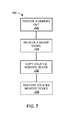
- FIG. 7 is a flow chart of a method of operation of the computing system in a further embodiment of the present invention.
- unit includes hardware in the present invention in accordance with the context in which the term is used.
- the hardware can include circuitry, programmable circuitry, computer, integrated circuit, integrated circuit cores, a pressure sensor, an inertial sensor, a microelectromechanical system (MEMS), passive devices, or a combination thereof.
- MEMS microelectromechanical system
- autonomous is defined as hardware capable of independently operating, responding, and reacting to an event or condition without assistance from any other hardware, software, or combination thereof, external to the hardware.
- Element names in the present invention having the term “command” is defined to always be hardware signals generated by hardware circuitry representing instructions, indicators, or information, sent and decoded by other hardware circuitry, unless specifically described as representing software.
- NVDIMM Non-volatile DIMM
- the NVDIMM monitors the CPU, memory controller clock, self-refresh, and power supplies and in the event of detected failures to intelligently and autonomously initiate DRAM self-refresh, switches the memory bus to the NVDIMM, and backs up DRAM data to flash.
- FIG. 1 therein is shown a computing system 100 with a memory unit 102 having a backup and recovery or restore mechanism in an embodiment of the present invention.
- the computing system 100 includes the memory unit 102 connecting to a compute unit 104 using an optional high-speed bi-directional link 108 .
- the memory unit 102 is shown having volatile memory devices 110 or DIMM devices, non-volatile memory devices 112 or NVDIMM devices having non-volatile memory, and a backup power unit 114 .
- the memory unit 102 includes circuitry for detection of an error or disruptive volatile memory events (DVME), backup of data in the volatile memory devices 110 to the non-volatile memory devices 112 before corruption of the data, and restoring of the volatile memory devices 110 with the data backed up from the non-volatile memory devices 112 in an autonomous and self-sustaining manner.
- DVME error or disruptive volatile memory events
- a DVME is defined as events external to the volatile memory devices 110 that could result in unintended loss of data previously stored in the volatile memory devices 110 .
- Examples of the DVME are the computing system 100 failures that can include an operating system (OS) crash, a central processor unit (CPU fault), a memory controller unit (MCU) failure, mother board (MB) internal power supply faults, a power loss, intermittent power drop-outs, or faults with system memory signals 118 to the volatile memory devices 110 .
- OS operating system
- CPU fault central processor unit
- MCU memory controller unit
- MB mother board
- Examples of the DVME are detected data errors from correctable or non-correctable coding schemes of linear block codes or convoluted codes.
- Examples of some the coding schemes are Error Correction Code (ECC), cyclic redundancy check (CRC) longitudinal redundancy check (LRC), Reed Solomon code (RSC), or parity errors.
- ECC Error Correction Code
- CRC cyclic redundancy check
- LRC longitudinal redundancy check
- RSC Reed Solomon code
- parity errors parity errors.
- Examples of the DVME for a dynamic random access memory can include control signals, such as bank address, memory controller clock, clock enable, chip select, data mask, RAS, CAS, WE, address, data strobe, or combinations thereof, sent to the DRAM that are ordered-out-of-sequence (OOS). Additional examples of the DVME for DRAMs can be detections of timing violations, such as set-up, hold, or skew violations between any combination of the system memory systems, system memory bus signals, self or auto refresh errors due to missing or invalid sequences, or a combination thereof. Further examples of DVME for DRAMs can include thermal warnings from the volatile memory devices 110 or remote thermal sensors with the memory unit 102 or the computing system 100 .
- the volatile memory devices 110 , the non-volatile memory devices 112 , and the backup power unit 114 are shown within the memory unit 102 . It is understood that the volatile memory devices 110 , the non-volatile memory devices 112 , the backup power unit 114 , or a combination thereof can be located external to the memory unit 102 .
- the volatile memory and the backup power unit 114 can be located within the compute unit 104 and the non-volatile memory devices 112 can be located in a room separate from a room having the memory unit 102 having circuitry used to process DVME and backup or restore the volatile memory devices 110 .
- the backup power unit 114 supplies power to the memory unit 102 and can include auxiliary remote backup power units (not shown) to provide power to any remotely located units or circuitry allocated to support functions of the memory unit 102 . Circuitry, components, and devices of the memory unit 102 physically at one location or distributed across different locations are self-sustaining and independent the compute unit 104 or other hardware not allocated for use by the memory unit 102 are independent.
- the memory unit 102 can operate without any power from other power sources other than the backup power unit 114 and any of the auxiliary remote backup power units allocated specifically for the memory unit 102 .
- the memory unit 102 automatically and independently monitors, detects, or snoops, the environment surrounding and connections to the volatile memory devices 110 to detect the DVME leading to the backup of the data into the non-volatile memory devices 112 from the volatile memory devices 110 .
- the term “snoop” is defined as a process whereby monitoring circuitry is electrically connected to signals or circuitry of hardware.
- the monitoring circuitry monitors and analyzes characteristics of the signals or the circuitry of the hardware for abnormalities.
- the snoop is performed as the signals or the circuitry of the hardware operate and without any impact to the operations or performance of the signals or the circuitry of the hardware.
- the computing system 100 is shown having the optional high-speed bi-directional link 108 . It is understood that the optional high-speed bi-directional link 108 could be omitted.
- the compute unit 104 and the memory unit 102 can be implemented in a single framed unit or cabinet to eliminate the need for the optional high-speed bi-directional link 108 .
- the optional high-speed bi-directional link 108 can be used to electrically connect the system memory bus 120 and the system memory control signals 118 of the compute unit 104 with storage memory bus 122 and storage memory control signals 124 of the memory unit 102 , respectively.
- the optional high-speed bi-directional link 108 can compensate for signal loss, timing, and skew between a location of the memory and a location of the compute unit 104 using a variety of connections methods.
- the computing system 100 configured without the optional high-speed bi-directional link 108 would result in the storage memory bus 122 and the storage memory control signals 124 of the memory unit 102 directly connected to the system memory bus 120 and the system memory control signals 118 of the compute unit 104 .
- the computer system includes a system power supply 126 dependent on external power sources and independent of the backup power unit 114 and computer components 128 used to provide functionality for the compute unit 104 .
- the memory unit 102 with the combination of the backup power unit 114 and the non-volatile memory devices 112 provides the computing system 100 with capabilities to detect conditions leading to loss of data in the volatile memory devices 110 and to preemptively backup the data before loss in to the non-volatile memory devices 112 in an independent and self-sustaining manner.
- the memory unit 102 with the combination of the backup power unit 114 and the non-volatile memory devices 112 provides the computing system 100 with capabilities to restore data from a DVME to the volatile memory devices 110 from the non-volatile memory devices 112 during a powering up of the computing system 100 without any hardware or software assistance from resources not previously designated for use by the memory unit 102 .
- the memory unit 102 with the combination of the backup power unit 114 and the non-volatile memory devices 112 during a powering-up of the computing system 100 restores data from the non-volatile memory devices 112 to the volatile memory devices 110 more efficiently than other computing systems which omit the functionalities or benefits of the backup power unit 114 and the non-volatile memory devices 112 managed by the memory unit 102 .
- FIG. 2 therein is shown an architecture diagram of the memory unit 102 of FIG. 1 .
- the architecture of the memory unit 102 can be implemented entirely in hardware with circuitry and can include software executed in the hardware, by the hardware with circuitry.
- Architectural functional units in the memory unit 102 providing for the backup or restore mechanisms can include a non-volatile controller unit 202 , a sync buffer unit 204 , a backup clock generator unit, the backup power unit 114 , the volatile memory devices 110 , the non-volatile memory devices 112 , and a mux unit 208 , also referred to as a multiplexor unit.
- the memory unit 102 is shown as an integral unit connecting directly to the system memory control signals 118 and the system memory bus 120 from the compute unit 104 of FIG. 1 without the optional high-speed bi-directional link 108 of FIG. 1 . It is understood that the optional high-speed bi-directional link 108 could be used to connect the memory unit 102 with the compute unit 104 when the memory unit 102 is located remotely from the compute unit 104 .
- the multiplexor unit is shown having two separate two-port to one-port pathway multiplexors with each port having any number of signals per port and controlled with mux path select signals 210 to control the path connections and direction between the six ports. It is understood that there can be any number of multiplexor units depending on the number of inputs or outputs of each multiplexor unit. For example, each multiplexor unit could have four-input ports and one-output port. In another example, each multiplexor unit could have eight-input ports and two-output ports.
- the volatile memory devices 110 are shown having a bi-directional data bus, shown and referred to as vm_bus 212 , used to receive write data to or send out data read from the volatile memory devices 110 .
- the volatile memory devices 110 also receive volatile memory control signals and a synchronized clock, shown and referred to as vm_cs 214 , used to control the operation and addressing of volatile memory of the volatile memory devices 110 .
- the non-volatile controller unit 202 also referred to as nv_controller unit, automatically connects the volatile memory devices 110 to the compute unit 104 during normal operations.
- the normal operations are defined as periods of operation when there are no detected disruptive volatile memory events, backup operations of data from the volatile memory devices 110 to the non-volatile memory devices 112 , or restore operations of data from the non-volatile memory devices 112 to the volatile devices using data and control buses of the non-volatile memory devices 112 , respectively labeled as nvm_bus 218 and nvm_c 220 .
- the non-volatile controller unit 202 automatically configures the memory unit 102 for normal operations by connecting the volatile memory devices 110 with the compute unit 104 by configuring the multiplexor unit to connect the vm_bus 212 with the system memory bus 120 and to connect the system memory control signals 118 with the vm_cs 214 signals of the volatile memory devices 110 through the sync buffer unit 204 .
- the non-volatile controller unit 202 can receive in-band commands, from the computing system 100 or outside the computing system, to automatically start a back up of all, or optionally a part of, the data in the volatile memory devices 110 to the non-volatile memory devices 112 .
- the in-band commands can be used for purposes of preempting any errors or faults, data archival purposes, data security procedural measures, or for any user defined application and executed without any intervention from hardware or software resources external to the memory unit 102 .
- the non-volatile controller unit 202 can detect error or fault signals and automatically perform back up of the data in the volatile memory devices 110 to the non-volatile memory devices 112 .
- the error or fault signals detected by the non-volatile controller unit 202 can include signals or indications from the power supplies, the CPU, thermal sensors, the compute unit 104 , or any device or unit within the computing system 100 .
- the non-volatile controller unit 202 can also detect errors based on abnormal signal sequences, electrical characteristics, or timing characteristics during the normal operations of the computing system 100 and automatically perform back up of the data in the volatile memory devices 110 to the non-volatile memory devices 112 .
- the abnormal signal sequences for example, can include timing violations, missing or extra signal transitions, improper or erratic signal voltage levels, signal noise, or a combination thereof.
- the non-volatile controller unit 202 automatically monitors, detects, snoops the error, the status, the control, or clock signals to detect abnormal conditions during the periods of normal operation.
- the abnormal conditions are defined as intermittent or continuous errors detected in hardware and can, for example, include timing violations, stuck or missing signals, activation of invalid or illegal signal combinations, clock variations or deviations, marginal signal voltage level swings, or any combination thereof of the control signals and clock.
- the sync buffer unit 204 can generate the vm_cs 214 signals from vm_i 222 signals to compensate for fanout, loading, and timing to the volatile memory devices 110 .
- the non-volatile controller unit 202 can independently monitor and compare the vm_cs 214 signals with the vm_i 222 signals. Through hardware handshake signals or hw_hs 216 , the non-volatile memory controller unit 202 can verify that the sync buffer unit 204 is operating properly, and on a miscompare, automatically back up data from the volatile memory devices 110 to the non-volatile memory devices 112 without intervention from hardware or software resources external to the memory unit 102 .
- the sync buffer unit 204 can be used to clock and synchronize the signals with an internal phase lock loop (PLL) to eliminate propagation delay times of control signals received from the multiplexor unit and improve drive strength to increase fan-out of the vm_cs 214 signals to the volatile memory devices 110 .
- PLL phase lock loop
- the sync buffer unit 204 can also include registers used to buffer the control signals.
- the non-volatile controller unit 202 is shown, receiving from the multiplexor unit, a copy of the control signals sent to the sync buffer unit 204 , shown and referred to as the vm_i 222 and vm_i_dup 228 , respectively. It is understood that the non-volatile controller unit 202 can receive any number of signals from within the memory unit 102 or the computing system 100 . For example, the non-volatile controller unit 202 can receive or monitor in-band commands, error, status signals, functional operation, or a combination thereof.
- Any of the abnormal conditions generates the disruptive volatile memory events (DVME) indication or condition used by the non-volatile controller unit 202 to automatically initiate a backup procedure of copying data in the volatile memory devices 110 to the non-volatile memory devices 112 .
- DVME disruptive volatile memory events
- the backup time period is defined as a maximum total time required by the non-volatile controller unit 202 to copy data from the volatile memory to the non-volatile memory of the non-volatile memory devices 112 before any of the data stored in the volatile memory is lost and includes DVME detection and processing times leading to the backup operation.
- the non-volatile controller unit 202 can configure the memory unit 102 to receive power from the backup power unit 114 and clocks from the backup clock generator unit, also referred to as a backup clock gen unit 230 , can prolong functionality of the memory unit 102 to provide a sufficient backup time period.
- the non-volatile controller unit 202 re-configures the multiplexor unit to connect a controller volatile memory input, shown and referred to cntlr_vm_i 224 , to the vm_i 222 input of the sync buffer unit 204 using the multiplexor unit. Activating and connecting the backup power unit 114 and the clocks to the memory unit 102 enables synchronous or clocked circuitry in the memory unit 102 to continue to operate.
- the synchronous circuitry in the memory unit 102 enables the non-volatile controller unit 202 to perform sequences and operations, as needed, to prevent loss of data over the duration of the backup time period based on type or characteristics of the volatile memory of the volatile memory devices 110 .
- the memory unit 102 could continue to receive the power and clocks from the compute unit 104 , as opposed to switching to power and clocks from the backup power unit 114 and the backup clock gen unit 230 , respectively.
- the volatile memory can be volatile semiconductor devices requiring refresh, such as synchronous dynamic random access memory (SDRAM), double data rate synchronous dynamic random access memory (DDR), or any superseding class types of DDR that can include DDR2, DDR3, DDR4 type devices. It is understood that the volatile memory can be other types of volatile memory that do not require refresh or refreshing.
- the volatile memory devices 110 could be static random access memory (SRAM) which retain data as-long-as power is maintained to the SRAM and do not require any refresh.
- SRAM static random access memory
- the non-volatile controller unit 202 places the volatile memory into a self-refresh operational mode. Sequences of the self-refresh applied to the clock and control signals by the non-volatile controller unit 202 can vary depending on the type, features, or manufacturer of the volatile memory of the memory unit 102 .
- the non-volatile controller unit 202 can prepare the non-volatile memory of the non-volatile memory devices 112 to receive and store data, also known as write data, from the volatile memory by reconfiguring the multiplexor unit to provide data bus paths from the volatile memory devices 110 to the non-volatile memory devices 112 .
- the non-volatile controller unit 202 can reconfigure the multiplexor unit to connect the vm_bus 212 to the cntlr_mem_bus, also referred to as the controller memory bus 232 , using the mux path select signals 210 .
- the non-volatile memory of the non-volatile memory devices 112 refers to flash memory, such as NAND flash memory. It is understood that the non-volatile memory or the non-volatile memory devices 112 can be of other types of readable/writable non-volatile memory devices.
- the non-volatile memory devices 112 could be data storage drives such as a hard disk drive (HDD), solid state drive (SSD), or a tape drive.
- Refresh times are defined as a total of all individual self-refresh cycles needed to guarantee the retention of all of the data stored in the volatile memory devices 110 until the data has been successfully copied over to the non-volatile memory devices 112 .
- the refresh times include the transitions times associated with each of the individual self-refresh cycles including times for the volatile memory devices 110 to switch from a normal operation mode to the self-refresh state until time when the volatile memory devices 110 are re-initialized and transitioned back to a condition ready for read or write operations.
- Interval times are defined as a total of all periods of time between successive periods of refresh, such as a self-refresh or auto refresh cycles, used by the non-volatile controller unit 202 to read or copy data from the volatile memory devices 110 to save or backup into the non-volatile memory devices 112 .
- the backup time period includes the totals of the refresh times, the interval times, overhead times such as configuration switching of the multiplexor unit, switching of the power sources, switching of the clock sources, and sequences performed by the non-volatile controller unit 202 .
- the non-volatile controller unit 202 includes timers to monitor and track the refresh times, the interval times, the backup time period, or any other events needed for proper sequencing or control of all operations associated with the memory unit 102 during the backup operations or any other times of operation.
- the data targeted in the volatile memory devices 110 to be backed-up is copied into the non-volatile memory devices 112 before the backup time period has elapsed.
- the backup time period can be used by the non-volatile controller unit 202 to indicate completion of a backup operation to the computing system 100 .
- the volatile memory unit can be restored with data from the non-volatile memory unit by the non-volatile controller unit 202 without intervention from hardware or software resources external to the memory unit 102 during a restore operation.
- the restore operation can be automatically performed by the non-volatile memory unit as a result of a power-up or an in-band command received from the computing system 100 .
- the non-volatile controller unit 202 can be configured to give warning prior to or prevent the restore operation if the cause of the most recent backup was from a DVME that has not been eliminated or addressed.
- the non-volatile controller unit 202 can determine if the DVME condition has been corrected by monitoring status, signals, or environment of the memory unit 102 and the computing system 100 as a condition for performing a restore operation.
- the non-volatile controller unit 202 automatically configures the multiplexor unit to connect the volatile memory bus with the controller memory bus 232 and to connect the controller volatile memory input with the volatile memory control signals, also referred to as the vm_cs 214 , of the volatile memory devices 110 through the sync buffer unit 204 for restoration operations.
- the non-volatile controller unit 202 can optionally configure the memory unit 102 to receive power from the backup power unit 114 or clocks from the backup clock gen unit 230 to restore data restoration in parallel or before the computing system 100 software OS, hardware resources, or any combination thereof is operational.
- the non-volatile controller unit 202 can automatically initialize the volatile memory devices 110 for write operations and the non-volatile memory devices 112 for read operations.
- the volatile memory devices 110 and the non-volatile memory devices 112 can be power sequenced up according their manufactured specifications.
- the non-volatile controller unit 202 can automatically configure bus paths within the memory unit 102 .
- the non-volatile controller unit 202 can configure the flow of data from the non-volatile memory devices 112 , through the non-volatile controller unit 202 , and to the volatile memory devices 110 .
- the non-volatile controller unit 202 can also perform refresh command operations, such as self-refresh or auto-refresh operations, to the volatile memory devices 110 on an as-needed-basis until the restoration or restore operations have completed.
- the non-volatile controller unit 202 can prepare the non-volatile memory while the volatile memory is self-refreshed to substantially reduce the total backup time period to copy data from the volatile memory to the non-volatile memory.
- the non-volatile controller unit 202 provides the memory unit 102 with the capability to autonomously perform backup operations of data from the volatile memory devices 110 to the non-volatile memory devices 112 without assistance from resources outside of the memory unit 102 in a self-managed, and self-sustaining manner.
- the non-volatile controller unit 202 provides the memory unit 102 with the capability to perform restoration of the volatile memory devices 110 with data from the non-volatile memory devices 112 without assistance from resources outside of the memory unit 102 , such as software, hardware, or operating system of the compute unit 104 .
- the non-volatile controller unit 202 provides the memory unit 102 with the capability to autonomously perform restoration of the volatile memory devices 110 with data from the non-volatile memory devices 112 without assistance from resources outside of the memory unit 102 in a self-managed, and self-sustaining manner.
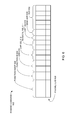
- FIG. 3 therein is shown an exemplary hardware block diagram of the memory unit 102 of FIG. 2 in the normal operating mode. Shown are field effect transistor (FET) multiplexors identified as fet mux1 302 and fet mux2 304 , smart register circuitry (S-REG) with a phase lock loop (PLL), also referred to as S-REG/PLL 306 , and DRAM hardware circuitry that can be used to implement and control the mux unit 208 of FIG. 2 , the sync buffer unit 204 , and the volatile memory devices 110 , respectively.
- FET field effect transistor
- S-REG smart register circuitry
- PLL phase lock loop
- DRAM DRAM hardware circuitry
- Connections such as wire or traces, are depicted as either solid lines or segmented lines having separated and alternating segment lengths.
- the solid lines indicate connections representative of the normal operating mode. It is understood that the segmented lines are connections disconnected by the FET multiplexors, such as the fet mux1 302 and the fet mux2 304 , monitored or snooped by circuitry and checked for a DVME condition, connections, monitored for a command or instructions from the computer unit, or any combination thereof.
- System power 308 such as VDDSPD, VDD, VDDQ, or other voltages, is received from the system power supply 126 of FIG. 1 of the compute unit 104 of FIG. 1 , for example, can include voltages seven hundred fifty millivolts, twelve hundred millivolts, fifteen hundred millivolts, eighteen hundred millivolts, twenty five hundred millivolts, or three hundred thirty millivolts.
- the system power 308 is selected and distributed throughout the memory unit 102 using memory unit power outputs, also referred to as mem_unit_pwr_o 310 , sent out of the backup power unit 114 .
- the DRAM can be read from, written to, and controlled by commands sent from the compute unit 104 using the clock and signals, such as address, commands, controls, and clock, sent from the compute unit to the S-REG using the fet mux2 304 .
- the S-REG with the PLL can be used to increase fan out of the bus signals by increasing signal drive strength of the bi-directional data to or from DRAM memory 312 , increase signal drive strength, or compensate for signal, address, or control bit skew.
- the S-REG can be also used to decode in-band commands received from the compute unit 104 through the system memory control signals 118 .
- the PLL and PLL associated circuitry of the S-REG can be used to functions as the backup clock gen unit 230 of FIG. 2 .
- the backup clock gen unit 230 can be implemented in hardware circuitry in other ways.
- the backup clock gen unit 230 can be hardware circuitry implemented and separated from the S-REG circuitry.
- the non-volatile controller unit 202 also referred to as a nv controller unit, is shown connected with the segmented lines to the hardware circuitry of the memory unit 102 and can include the backup power unit 114 , the volatile memory devices 110 , the sync buffer unit 204 , the fet mux1 302 , the fet mux2 304 , and the non-volatile memory devices 112 with a bypass mux 314 .
- the non-volatile controller unit 202 can include the hardware circuitry for a dvme_detect/ind 318 , a mu_controller 320 , a vm_sequencer 322 , an endec_cdr 324 , a nvm_sequencer 328 , and a mu_sys_intf 330 .
- the nv controller unit intelligently and automatically monitors for the events in the computing system 100 of FIG. 1 that can result in loss of data 331 stored in the volatile memory devices 110 .
- the nv controller unit can automatically re-configure the memory unit 102 and backup the data 331 stored in the volatile memory devices 110 as a result of a detected DVME or an in-band backup command received using a mu_comm_intf 348 from the compute unit 104 or an optional remote device, also referred to as opt_rmt_dev 332 , outside the computing system 100 .
- the nv controller unit can automatically re-configure the memory unit 102 and backup the data 331 without hardware or software assistance from resources not previously designated for use by the memory unit 102 and without the system power 308 from the compute unit 104 .
- the mu_controller 320 also referred to as the memory unit controller, is hardware circuitry used to receive, filter, consolidate, and analyze events received from status signals 334 within the computing system 100 and monitored by the mu_controller 320 of the non-volatile controller unit 202 , described in FIG. 2 .
- the status signals 334 are outputs from circuitry or sensors from different functional areas used by the non-volatile controller unit 202 to indicate localized conditions within each of the different functional areas.
- the mu_controller 320 can be connected to the S-REG using a bi-directional communication path, such as an I2c, a proprietary interface, or a system management bus (SMBus).
- the bi-directional communication path can be used by the mu_controller 320 to snoop the signals from the S-REG to the DRAM memory 312 for proper operation, such as conformance to joint electron devices engineering council (JEDEC) DRAM defined self-refresh state or to permit the mu_controller 320 to send commands to the S-REG for self-refresh and prevent any new commands from prematurely taking the DRAM memory 312 out of the self-refresh state.
- JEDEC joint electron devices engineering council
- the bi-directional communication path is the hw_hs 216 .
- the dvme 318 or dvme_detect/ind 318 is hardware circuitry operatively integral with the S-REG/PLL 306 and the nv_controller unit 202 .
- the dvme 318 or dvme_detect/ind 318 uses snoop signals 319 to detect specific errors with the system memory control signals 118 sent from the S-REG with PLL to the volatile memory devices 110 .
- the vm_sequencer 322 also referred to as the volatile memory sequencer, can be readied to deliver memory signals to the fet mux2 304 in the event of a backup volatile memory operation or a restore volatile memory operation.
- the data 331 stored into the DRAM memory 312 by the computing unit can include an ECC for purposes of detecting, correcting, or a combination thereof, the data 331 .
- ECC for purposes of detecting, correcting, or a combination thereof
- eight bits of ECC can be included with every sixty-four bits of the data 331 to detect and correct errors from reading or writing the DRAM memory 312 .
- the endec_cdr 324 hardware circuitry is an encoder and decoder for the coding schemes that optionally may have been included with the data 331 written from the system memory bus 120 to the volatile memory.
- the circuitry of the endec_cdr 324 can be used to check and generate coding schemes during a backup volatile memory operation, a restore volatile memory operation, a read or write of data of the non-volatile memory devices 112 , or a combination thereof.
- the circuitry of the endec_cdr 324 can also provide additional levels of data detection and correction capabilities by applying another level of coding schemes.
- hardware circuitry of the endec_cdr 324 could apply a reed Solomon encoder of eight bits for every five hundred and forty bytes of ECC that the system provided, such as the eight bits of ECC can be included with every sixty-four bits of the data 331 , to be included in the data 331 as the data 331 is written to the non-volatile memory devices 112 .
- the reed Solomon encoded data can be decoded, checked, corrected if needed, and removed by the circuitry of the endec_cdr 324 prior to re-writing of the data 331 , with the eight bits of ECC included with every sixty-four bits of the data 331 , back into the volatile memory devices 110 .
- the bypass mux 314 can be used to bypass the circuitry of the endec_cdr 324 if the data 331 written from the system memory bus 120 to the volatile memory is without any coding schemes.
- the nvm_sequencer 328 also referred to as the non-volatile memory sequencer, is hardware circuitry readied to actively deliver non-volatile memory signals to the non-volatile memory devices 112 in the event of a backup volatile memory operation or a restore volatile memory operation.
- the mu_sys_intf 330 also referred to as the memory unit system interface, is hardware circuitry used to create communication interfaces between the nv_controller unit and circuitry external to the nv_controller unit.
- the communication interfaces can include parallel interfaces or serial interfaces such as inter-integrated circuit or two-wire interfaces (I2C) interfaces.
- the serial interfaces can include serial presence detector SPD I2C interfaces, a backup I2C interface, a state control interface, or a combination thereof.
- the SPD I2C interfaces can be used to determine type or characteristics of a memory module.
- the backup power unit 114 can include a power sense and control circuit, a power rail switch, and a backup power source supplying power, also shown and referred to as pwr sns/cntl 338 , pwr_rail switch 340 , and bakup_pwr_src 342 , respectively, allocated for use by the memory unit 102 to monitor and sense various voltages received from the compute unit 104 .
- NVDIMM non-volatile flash DIMM
- a memory controller such as the non-volatile controller unit 202 or FPGA, completes all active memory cycles (closes all open rows and banks) and activates signals to trigger self-refresh of the DRAMs.
- the memory controller allocates fixed worst case delays for handshaking signals and processing to insure that the self-refresh has begun.
- the memory controller switches multiplexors, such as analog multiplexors or FETs to configure the connections to/from the NVDIMMs and DRAMs, can be used to quickly re-configure signals and busses between the mu_controller 320 and portions of the memory unit 102 surrounding the mu_controller 320 .
- the memory controller deactivates signals triggering the self-refresh.
- the memory controller processes and controls the actual transfer of data, synchronization, and clocking and periodic self-refresh cycles as needed throughout the backup operation until completion.
- registers of the NVDIMM initiates self-refresh process of DRAMs by generating signals to start a self-refresh.
- the registers handshake to the memory controller that self-refresh is active and operating.
- the memory controller receives handshake from the registers and proceeds to switch the FETs of multiplexors.
- the memory controller completes configuring the multiplexors and deactivates the self-refresh to guarantee the clock signals have properly transitioned and back-up can be enabled. Further self-refresh cycles are repeated in the same manner until backup of the DRAM has completed.
- registers of the NVDIMM can receive and decode in-band information, such as an address, a command, and a control bus information, to initiate a backup event request.
- the in-band function for example, can be a “save” function as shown and defined in FIG. 6 .
- the “save” function results in the NVDIMM placing the DRAM in to a self-refresh mode.
- the registers of the NVDIMM sends handshaking signals to indicate to the memory controller the activation of the self-refresh.
- the memory controller switches the FETs and controls the DRAM to back-up of information from the DRAM to the NVDIMM between self-refresh cycle deactivations as indicated by the handshaking signals. Further self-refresh cycles are indicated to the memory controller to permit the memory controller to switch between backup and switch re-configuring of the FETs until the back-up process has completed.
- FIG. 3 depicts the FET multiplexors, the sync buffer unit 204 , the backup power unit 114 , the nv controller unit, the bypass mux 314 , the volatile memory devices 110 , and the non-volatile memory devices 112 as separate units of hardware circuitry. It is understood that the separate units can be combined or separated in hardware in differently.
- the separate units could be combined, for example, to include all of the separate units into three field programmable gate array devices (FPGA).
- FPGA field programmable gate array devices
- only the nv controller unit and the bypass mux 314 could be integrated into a single FPGA.
- the power sense and control and the power rail switch could be implemented into an application specific integrated circuit (ASIC) module with the backup power unit 114 located external from the ASIC.
- ASIC application specific integrated circuit
- the non-volatile memory devices 112 are shown as open standards ONFI NAND flash type memory, also referred to as ONFI NAND flash 344 . It is understood that the memory unit 102 can have other types of non-volatile memory devices.
- the non-volatile memory devices 112 could be a HDD.
- the volatile memory devices 110 are depicted having four of the DRAM memory 312 and the non-volatile memory devices 112 are depicted having four of the ONFI NAND flash 344 . It is understood that there can be any number of the DRAM memory 312 or the ONFI NAND flash 344 .
- the volatile memory devices 110 can include sixteen of the DRAM memory 312 and the non-volatile device can include eight of the ONFI NAND flash 344 .
- the mu_controller 320 and the dvme detector and indicator circuitry having monitored or snooped information from the vm_sequencer 322 or the hw_hs 216 interface provides the non-volatile controller unit 202 the capability to not only backup the data 331 in the volatile memory devices 110 but also record detailed information as to what the data 331 may or could have been corrupted by the error or disruptive volatile memory event resulting in no data integrity issues and what the data 331 is correct versus might not be correct.
- the mu_controller 320 detects at least one DVME or an in-band backup command to backup data. Shown are the sync buffer unit 204 , the S-REG/PLL 306 , the system memory control signals 118 , the pwr sns/cntl 338 , the bakup_pwr_src 342 , the pwr_rail switch 340 , the dvme 318 , the dvme_detect/ind 318 , and the non-volatile controller unit 202 .
- the opt_rmt_dev 332 the status signals 334 , the mem_unit_pwr_o 310 , and the volatile memory devices 110 with the data 331 to be backed up into the non-volatile memory devices 112 , and the ONFI NAND flash 344 .
- the system power 308 connecting to the backup power unit 114 is shown having segmented lines to indicate that the system power 308 is not used and the backup power unit 114 is selected to generate the memory unit power outputs using the power rail switch. If no DVME is detected by the mu_controller 320 , it is understood that the system power 308 could have continued to be selected, as in the normal operating mode, to generate the memory unit power outputs.
- the solid lines are used to indicate connections established within the memory unit 102 as a result of the DVME.
- the PLL within the S-REG continues to operate and is distributed to the hardware circuitry of the memory unit 102 .
- the vm_sequencer 322 generates and sends sequences through the fet mux2 304 and the sync buffer unit 204 to the DRAM memory 312 .
- the DRAM memory 312 is immediately placed into self-refresh mode by the mu_controller 320 to preserve the data 331 previously written into the DRAM memory 312 with no dependency of a clock to the DRAM.
- the hw_hs 216 of the mu_controller 320 or the vm_sequencer 322 can be used to place or control the self-refresh of the DRAM memory 312 .
- the self-refresh mode is defined as low powered down state of the DRAM where internal data of the DRAM is preserved, minimum power is continuously applied to the DRAM, and access to the internal data is not permitted until the DRAM is re-restored to a normal powered up and initialized state using a powerup/initialization operation described in FIG. 5 .
- the mu_controller 320 can use the hw_hs 216 , or instruct the nvm_sequencer 328 , to initialize and prepare the ONFI NAND flash 344 for data write operations. Also, the mu_controller 320 configures the fet mux1 302 , the bypass mux 314 , and if appropriate, the endec_cdr 324 circuitry for data to be read from the DRAM memory 312 to the ONFI NAND flash 344 .
- the DRAM memory 312 is powered up and initialized for read operations.
- the mu_controller 320 copies the data from the DRAM memory 312 to the ONFI NAND flash 344 to perform the backup operation.
- sequences involved for the backup operation may vary due to the data size, data structure, and physical configuration or specifications of the DRAM memory 312 and the ONFI NAND flash 344 .
- the nv_controller unit can sequence down the memory unit 102 and power off the memory unit 102 or perform further operations optionally sent as in-band commands through mu communication interfaces, also referred to as the mu_comm_intf 348 , from circuitry of the mu_sys_intf 330 .
- the mu_sys_intf 330 circuitry provides the communication interfaces between the nv controller unit and the computing system 100 or the optional remote device outside the computing system 100 .
- the mu communication interfaces can include a backup I2C interface, a SPD I2C interface, a general I2C interface, a parallel interface, an interface of control, address, data, or select signals, or any combination thereof.
- the optional remote device can be another computing system, a smart phone, or any electronic device coupled to the mu communication interfaces through wire, wireless, optical, transport layers, or any form of remote communication and connection medium.
- the restore operating mode can be automatically executed without any intervention from hardware or software resources external to the memory unit 102 .
- the restore operating mode can begin as a result of the computing system 100 power-up or an in-band command received by the memory unit 102 from the computing system 100 of FIG. 1 , the mu communication interfaces, or the optional remote device.
- the pwr sns/cntl 338 the bakup_pwr_src 342 , the pwr_rail switch 340 , the mem_unit_pwr_o 310 , the mu_comm_intf 348 , the opt_rmt_dev 332 , the nvm_sequencer 328 , the endec_cdr 324 , the vm_sequencer 322 , the mu_controller 320 , the dvme 318 , the dvme_detect/ind 318 , the mu_sys_intf 330 , and the status signals 334 .
- the nv_controller unit configures the fet mux1 302 , the fet mux2 304 , and the bypass mux 314 to connect the data paths between the ONFI NAND flash 344 and the DRAM memory 312 .
- the nv_controller unit configures the ONFI NAND flash 344 for read data operations and the DRAM memory 312 for write data operations to restore the data 331 back from the ONFI NAND flash 344 .
- the DRAM memory 312 and the ONFI NAND flash 344 are powered-up and initialized using either the system power 308 or the backup power source from the backup power unit 114 .
- the system power 308 is expected to be available and stable.
- the backup power unit 114 can switch from the backup power source to the system power 308 .
- the backup power unit 114 could deliver power from the backup power unit 114 to ready the DRAM memory 312 before the computing unit has completed boot-up.
- the memory unit 102 with the combination of the backup power source of the backup power unit 114 , the non-volatile controller unit 202 , the FET multiplexors, the sync buffer unit 204 , the bypass mux 314 , and the ONFI NAND flash 344 , and the DRAM memory 312 , results in a significantly faster powerup to functional availability time of the computing system 100 over an availability time of a computing system, excluding the memory unit 102 of the present invention to be powerup and functionally available for operation.
- FIG. 6 therein is shown an example of an in-band initiated command 602 . Shown is a portion of the in-band initiated command, such as a backup command, that can be received by the memory unit 102 of FIG. 1 from the system memory bus 120 of FIG. 1 of the compute unit 104 of FIG. 1 or the mu_comm_intf 348 of FIG. 3 .
- the backup command can be function name 604 and function id 606 , such as “save” and “sv”, respectively.
- the backup command can include a specification of parameters 608 such as clock enables 610 , chip selects 612 , row/column address selects 614 , write enable 618 , bank adr 620 , and addr 622 signals to be sent to the non-volatile memory devices 112 of FIG. 1 to physically control, program, or identify the non-volatile memory devices 112 .
- a recover or a restore command can be constructed, defined, and implemented to initiate the restore operation.
- Extra or different parameters fields can be added, substituted, or changed for specific types of the non-volatile memory devices 112 and operations.
- the method 700 includes: providing a memory unit having a volatile memory device with data and a non-volatile controller unit in a block 702 ; receiving a snoop signal sent to a memory unit controller of the non-volatile controller unit for indicating an error in a block 704 ; copying the data of the volatile memory device, synchronously, to a non-volatile device of the memory unit based on the snoop signal, the data autonomously copied without any intervention from outside the memory unit to prevent loss of the data in a block 706 ; and restoring the data, based on an in-band command received by the memory unit, to autonomously restore the data of the volatile memory device from the non-volatile device without any intervention from outside the memory unit in a block 708 .
- the computing system 100 furnishes important and heretofore unknown and unavailable solutions, capabilities, and functional aspects.
- the resulting method, process, apparatus, device, product, and/or system is straightforward, cost-effective, uncomplicated, highly versatile and effective, can be surprisingly and unobviously implemented by adapting known technologies, and are thus readily suited for efficiently and economically manufacturing the present invention compatible with conventional manufacturing methods or processes and technologies.
- Another important aspect of the present invention is that it valuably supports and services the historical trend of reducing costs, simplifying systems, and increasing performance.
- the asynchronous faults can include a CPU fault that makes it impossible for the NVDIMM DRAMs to be placed into self-refresh before the NVDIMM backup is triggered.
- the NVDIMM register device must be capable of autonomously placing the DRAM devices into self-refresh either by acting on a signal from the NVDIMM or NVDIMM FPGA.
- the signal is triggered by NVDIMM power failure detection, an external signal, detection of a failed clock signal from the memory controller, or failure by the memory controller.
- the NVDIMM register device must be capable of issuing a self-refresh command within a predetermined interval.
Abstract
Description
Claims (20)
Priority Applications (1)
| Application Number | Priority Date | Filing Date | Title |
|---|---|---|---|
| US13/940,118 US9779016B1 (en) | 2012-07-25 | 2013-07-11 | Computing system with backup and recovery mechanism and method of operation thereof |
Applications Claiming Priority (2)
| Application Number | Priority Date | Filing Date | Title |
|---|---|---|---|
| US201261675776P | 2012-07-25 | 2012-07-25 | |
| US13/940,118 US9779016B1 (en) | 2012-07-25 | 2013-07-11 | Computing system with backup and recovery mechanism and method of operation thereof |
Publications (1)
| Publication Number | Publication Date |
|---|---|
| US9779016B1 true US9779016B1 (en) | 2017-10-03 |
Family
ID=59928508
Family Applications (1)
| Application Number | Title | Priority Date | Filing Date |
|---|---|---|---|
| US13/940,118 Active 2034-11-04 US9779016B1 (en) | 2012-07-25 | 2013-07-11 | Computing system with backup and recovery mechanism and method of operation thereof |
Country Status (1)
| Country | Link |
|---|---|
| US (1) | US9779016B1 (en) |
Cited By (23)
| Publication number | Priority date | Publication date | Assignee | Title |
|---|---|---|---|---|
| US20170052850A1 (en) * | 2015-08-21 | 2017-02-23 | Fanuc Corporation | Numerical controller |
| US20170344288A1 (en) * | 2016-05-30 | 2017-11-30 | Silicon Motion, Inc. | Data storing method and system initinalizing method after sudden power-off event |
| US9921980B2 (en) | 2013-08-12 | 2018-03-20 | Micron Technology, Inc. | Apparatuses and methods for configuring I/Os of memory for hybrid memory modules |
| US10152393B2 (en) * | 2016-08-28 | 2018-12-11 | Microsoft Technology Licensing, Llc | Out-of-band data recovery in computing systems |
| US10216685B1 (en) * | 2017-07-19 | 2019-02-26 | Agiga Tech Inc. | Memory modules with nonvolatile storage and rapid, sustained transfer rates |
| US20190155702A1 (en) * | 2015-12-22 | 2019-05-23 | EMC IP Holding Company LLC | Asymmetric memory transceiver |
| WO2019157057A1 (en) * | 2018-02-08 | 2019-08-15 | Micron Technology, Inc | Backup operations from volatile to non-volatile memory |
| US10551892B1 (en) * | 2017-09-19 | 2020-02-04 | Smart Modular Technologies, Inc. | Centralized backup power module |
| US10567501B2 (en) * | 2016-03-29 | 2020-02-18 | Lsis Co., Ltd. | Energy management server, energy management system and the method for operating the same |
| CN111090387A (en) * | 2018-10-24 | 2020-05-01 | 三星电子株式会社 | Memory module, method of operating the same, and method of operating host controlling the same |
| US10782759B1 (en) | 2019-04-23 | 2020-09-22 | Arbor Company, Lllp | Systems and methods for integrating batteries with stacked integrated circuit die elements |
| US10802735B1 (en) | 2019-04-23 | 2020-10-13 | Arbor Company, Lllp | Systems and methods for reconfiguring dual-function cell arrays |
| WO2020236379A1 (en) * | 2019-05-21 | 2020-11-26 | Arbor Company Lllp | Systems and methods for integrating batteries with stacked integrated circuit die elements |
| WO2020255087A1 (en) * | 2019-06-20 | 2020-12-24 | Smolka John Michael | Memory module and processor contained in the memory module |
| US10976940B2 (en) * | 2017-12-14 | 2021-04-13 | International Business Machines Corporation | Copy source to target management in a data storage system |
| US10990463B2 (en) | 2018-03-27 | 2021-04-27 | Samsung Electronics Co., Ltd. | Semiconductor memory module and memory system including the same |
| US11054994B2 (en) | 2017-12-14 | 2021-07-06 | International Business Machines Corporation | Copy source to target management in a data storage system |
| US20220113912A1 (en) * | 2019-06-10 | 2022-04-14 | Ngd Systems, Inc. | Heterogeneous in-storage computation |
| US11463524B2 (en) | 2020-06-29 | 2022-10-04 | Arbor Company, Lllp | Mobile IoT edge device using 3D-die stacking re-configurable processor module with 5G processor-independent modem |
| US11500728B2 (en) | 2020-11-27 | 2022-11-15 | Samsung Electronics Co., Ltd. | Storage controller and method of restoring error of the same |
| WO2023183133A1 (en) | 2022-03-24 | 2023-09-28 | Smart Modular Technologies, Inc. | Serial attached non-volatile memory |
| US11797225B2 (en) * | 2016-01-19 | 2023-10-24 | Lodestar Licensing Group, Llc | Non-volatile memory module architecture to support memory error correction |
| US20230342047A1 (en) * | 2022-04-21 | 2023-10-26 | Micron Technology, Inc. | Self-Refresh Arbitration |
Citations (12)
| Publication number | Priority date | Publication date | Assignee | Title |
|---|---|---|---|---|
| US5799200A (en) | 1995-09-28 | 1998-08-25 | Emc Corporation | Power failure responsive apparatus and method having a shadow dram, a flash ROM, an auxiliary battery, and a controller |
| US6529945B1 (en) * | 1999-07-26 | 2003-03-04 | International Business Machines Corporation | Data buffer management between two different systems |
| US20040093538A1 (en) * | 2002-11-07 | 2004-05-13 | International Business Machines Corporation | Method and apparatus for obtaining diagnostic data for a device attached to a computer system |
| US20060168471A1 (en) * | 2005-01-25 | 2006-07-27 | Schulstad Geir O | Automatically triggered snapshot data dump for storage unit with embedded system |
| US20070168740A1 (en) * | 2006-01-10 | 2007-07-19 | Telefonaktiebolaget Lm Ericsson (Publ) | Method and apparatus for dumping a process memory space |
| US20070208905A1 (en) * | 2006-03-06 | 2007-09-06 | Ramot At Tel-Aviv University Ltd. | Multi-bit-per-cell flash memory device with non-bijective mapping |
| US20090235038A1 (en) * | 2007-07-25 | 2009-09-17 | Agiga Tech Inc. | Hybrid memory system with backup power source and multiple backup an restore methodology |
| US20100205348A1 (en) * | 2009-02-11 | 2010-08-12 | Stec, Inc | Flash backed dram module storing parameter information of the dram module in the flash |
| US20110131475A1 (en) * | 2009-12-01 | 2011-06-02 | Canon Kabushiki Kaisha | Method for determining a copy to be decoded and an associated erasures vector, corresponding storage means and receiver device |
| US20120089796A1 (en) | 2010-10-12 | 2012-04-12 | Hitachi, Ltd. | Memory data backup system and memory data backup control method |
| US8301833B1 (en) | 2007-06-01 | 2012-10-30 | Netlist, Inc. | Non-volatile memory module |
| US8607023B1 (en) * | 2009-12-16 | 2013-12-10 | Applied Micro Circuits Corporation | System-on-chip with dynamic memory module switching |
-
2013
- 2013-07-11 US US13/940,118 patent/US9779016B1/en active Active
Patent Citations (12)
| Publication number | Priority date | Publication date | Assignee | Title |
|---|---|---|---|---|
| US5799200A (en) | 1995-09-28 | 1998-08-25 | Emc Corporation | Power failure responsive apparatus and method having a shadow dram, a flash ROM, an auxiliary battery, and a controller |
| US6529945B1 (en) * | 1999-07-26 | 2003-03-04 | International Business Machines Corporation | Data buffer management between two different systems |
| US20040093538A1 (en) * | 2002-11-07 | 2004-05-13 | International Business Machines Corporation | Method and apparatus for obtaining diagnostic data for a device attached to a computer system |
| US20060168471A1 (en) * | 2005-01-25 | 2006-07-27 | Schulstad Geir O | Automatically triggered snapshot data dump for storage unit with embedded system |
| US20070168740A1 (en) * | 2006-01-10 | 2007-07-19 | Telefonaktiebolaget Lm Ericsson (Publ) | Method and apparatus for dumping a process memory space |
| US20070208905A1 (en) * | 2006-03-06 | 2007-09-06 | Ramot At Tel-Aviv University Ltd. | Multi-bit-per-cell flash memory device with non-bijective mapping |
| US8301833B1 (en) | 2007-06-01 | 2012-10-30 | Netlist, Inc. | Non-volatile memory module |
| US20090235038A1 (en) * | 2007-07-25 | 2009-09-17 | Agiga Tech Inc. | Hybrid memory system with backup power source and multiple backup an restore methodology |
| US20100205348A1 (en) * | 2009-02-11 | 2010-08-12 | Stec, Inc | Flash backed dram module storing parameter information of the dram module in the flash |
| US20110131475A1 (en) * | 2009-12-01 | 2011-06-02 | Canon Kabushiki Kaisha | Method for determining a copy to be decoded and an associated erasures vector, corresponding storage means and receiver device |
| US8607023B1 (en) * | 2009-12-16 | 2013-12-10 | Applied Micro Circuits Corporation | System-on-chip with dynamic memory module switching |
| US20120089796A1 (en) | 2010-10-12 | 2012-04-12 | Hitachi, Ltd. | Memory data backup system and memory data backup control method |
Cited By (38)
| Publication number | Priority date | Publication date | Assignee | Title |
|---|---|---|---|---|
| US11886754B2 (en) | 2013-08-12 | 2024-01-30 | Lodestar Licensing Group Llc | Apparatuses and methods for configuring I/Os of memory for hybrid memory modules |
| US11379158B2 (en) | 2013-08-12 | 2022-07-05 | Micron Technology, Inc. | Apparatuses and methods for configuring I/Os of memory for hybrid memory modules |
| US9921980B2 (en) | 2013-08-12 | 2018-03-20 | Micron Technology, Inc. | Apparatuses and methods for configuring I/Os of memory for hybrid memory modules |
| US10698640B2 (en) | 2013-08-12 | 2020-06-30 | Micron Technology, Inc. | Apparatuses and methods for configuring I/Os of memory for hybrid memory modules |
| US10423363B2 (en) | 2013-08-12 | 2019-09-24 | Micron Technology, Inc. | Apparatuses and methods for configuring I/OS of memory for hybrid memory modules |
| US20170052850A1 (en) * | 2015-08-21 | 2017-02-23 | Fanuc Corporation | Numerical controller |
| US10042712B2 (en) * | 2015-08-21 | 2018-08-07 | Fanuc Corporation | Numerical controller |
| US20190155702A1 (en) * | 2015-12-22 | 2019-05-23 | EMC IP Holding Company LLC | Asymmetric memory transceiver |
| US10776222B2 (en) * | 2015-12-22 | 2020-09-15 | EMC IP Holding Company LLC | Asymmetric memory transceiver |
| US11797225B2 (en) * | 2016-01-19 | 2023-10-24 | Lodestar Licensing Group, Llc | Non-volatile memory module architecture to support memory error correction |
| US10567501B2 (en) * | 2016-03-29 | 2020-02-18 | Lsis Co., Ltd. | Energy management server, energy management system and the method for operating the same |
| US10817188B2 (en) * | 2016-05-30 | 2020-10-27 | Silicon Motion, Inc. | Data storing method and system initializing method after sudden power-off event |
| US20170344288A1 (en) * | 2016-05-30 | 2017-11-30 | Silicon Motion, Inc. | Data storing method and system initinalizing method after sudden power-off event |
| US10152393B2 (en) * | 2016-08-28 | 2018-12-11 | Microsoft Technology Licensing, Llc | Out-of-band data recovery in computing systems |
| US10216685B1 (en) * | 2017-07-19 | 2019-02-26 | Agiga Tech Inc. | Memory modules with nonvolatile storage and rapid, sustained transfer rates |
| US10551892B1 (en) * | 2017-09-19 | 2020-02-04 | Smart Modular Technologies, Inc. | Centralized backup power module |
| US10976940B2 (en) * | 2017-12-14 | 2021-04-13 | International Business Machines Corporation | Copy source to target management in a data storage system |
| US11054994B2 (en) | 2017-12-14 | 2021-07-06 | International Business Machines Corporation | Copy source to target management in a data storage system |
| WO2019157057A1 (en) * | 2018-02-08 | 2019-08-15 | Micron Technology, Inc | Backup operations from volatile to non-volatile memory |
| US10990463B2 (en) | 2018-03-27 | 2021-04-27 | Samsung Electronics Co., Ltd. | Semiconductor memory module and memory system including the same |
| CN111090387B (en) * | 2018-10-24 | 2023-07-28 | 三星电子株式会社 | Memory module, method of operating the same, and method of operating host controlling the same |
| US10884655B2 (en) | 2018-10-24 | 2021-01-05 | Samsung Electronics Co., Ltd. | Storage modules, methods of operating a storage module, and methods of operating a host controlling a storage module |
| CN111090387A (en) * | 2018-10-24 | 2020-05-01 | 三星电子株式会社 | Memory module, method of operating the same, and method of operating host controlling the same |
| US10802735B1 (en) | 2019-04-23 | 2020-10-13 | Arbor Company, Lllp | Systems and methods for reconfiguring dual-function cell arrays |
| US11061455B2 (en) | 2019-04-23 | 2021-07-13 | Arbor Company, Lllp | Systems and methods for integrating batteries with stacked integrated circuit die elements |
| US10969977B2 (en) | 2019-04-23 | 2021-04-06 | Arbor Company, Lllp | Systems and methods for reconfiguring dual function cell arrays |
| US10782759B1 (en) | 2019-04-23 | 2020-09-22 | Arbor Company, Lllp | Systems and methods for integrating batteries with stacked integrated circuit die elements |
| US11435800B2 (en) | 2019-04-23 | 2022-09-06 | Arbor Company, Lllp | Systems and methods for reconfiguring dual-function cell arrays |
| US11797067B2 (en) | 2019-04-23 | 2023-10-24 | Arbor Company, Lllp | Systems and methods for reconfiguring dual-function cell arrays |
| WO2020236379A1 (en) * | 2019-05-21 | 2020-11-26 | Arbor Company Lllp | Systems and methods for integrating batteries with stacked integrated circuit die elements |
| CN114402271A (en) * | 2019-05-21 | 2022-04-26 | 乔木有限责任合伙公司 | System and method for integrating a battery with stacked integrated circuit die elements |
| US20220113912A1 (en) * | 2019-06-10 | 2022-04-14 | Ngd Systems, Inc. | Heterogeneous in-storage computation |
| WO2020255087A1 (en) * | 2019-06-20 | 2020-12-24 | Smolka John Michael | Memory module and processor contained in the memory module |
| US11463524B2 (en) | 2020-06-29 | 2022-10-04 | Arbor Company, Lllp | Mobile IoT edge device using 3D-die stacking re-configurable processor module with 5G processor-independent modem |
| US11895191B2 (en) | 2020-06-29 | 2024-02-06 | Arbor Company, Lllp | Mobile IoT edge device using 3D-die stacking re-configurable processor module with 5G processor-independent modem |
| US11500728B2 (en) | 2020-11-27 | 2022-11-15 | Samsung Electronics Co., Ltd. | Storage controller and method of restoring error of the same |
| WO2023183133A1 (en) | 2022-03-24 | 2023-09-28 | Smart Modular Technologies, Inc. | Serial attached non-volatile memory |
| US20230342047A1 (en) * | 2022-04-21 | 2023-10-26 | Micron Technology, Inc. | Self-Refresh Arbitration |
Similar Documents
| Publication | Publication Date | Title |
|---|---|---|
| US9779016B1 (en) | Computing system with backup and recovery mechanism and method of operation thereof | |
| TWI710892B (en) | Method for correcting error of dram | |
| US8892942B2 (en) | Rank sparing system and method | |
| US7320086B2 (en) | Error indication in a raid memory system | |
| US6785835B2 (en) | Raid memory | |
| US6684292B2 (en) | Memory module resync | |
| US6854070B2 (en) | Hot-upgrade/hot-add memory | |
| US6766469B2 (en) | Hot-replace of memory | |
| KR101710546B1 (en) | Memory power management | |
| US8745323B2 (en) | System and method for controller independent faulty memory replacement | |
| US9317366B2 (en) | Protocol checking logic circuit for memory system reliability | |
| US20100106904A1 (en) | Shadow raid cache memory | |
| US8020053B2 (en) | On-line memory testing | |
| US6981173B2 (en) | Redundant memory sequence and fault isolation | |
| KR20170130384A (en) | Dynamic application of ECC based on error type | |
| US6640282B2 (en) | Hot replace power control sequence logic | |
| US20030208654A1 (en) | Computer system architecture with hot pluggable main memory boards | |
| US9684520B2 (en) | Computing system with non-disruptive fast memory restore mechanism and method of operation thereof | |
| JP6282482B2 (en) | Programmable circuit device and configuration information restoration method | |
| WO2014099021A1 (en) | Multiple computer system processing write data outside of checkpointing | |
| US20090089514A1 (en) | Implementing Asynchronous Request for Forcing Dynamic Memory into Self Refresh | |
| WO2023183133A1 (en) | Serial attached non-volatile memory | |
| WO2016164033A1 (en) | Partial backup during runtime for memory modules with volatile memory and non-volatile memory | |
| US10747611B2 (en) | Safety enhancement for memory controllers | |
| US10592364B2 (en) | Handling errors during run time backups |
Legal Events
| Date | Code | Title | Description |
|---|---|---|---|
| AS | Assignment |
Owner name: SMART MODULAR TECHNOLOGIES, INC., CALIFORNIA Free format text: ASSIGNMENT OF ASSIGNORS INTEREST;ASSIGNORS:SHEN, JINGYING;FREY, ROBERT TOWER;MARINO, KELVIN;SIGNING DATES FROM 20130708 TO 20130709;REEL/FRAME:030782/0362 |
|
| AS | Assignment |
Owner name: SMART MODULAR TECHNOLOGIES, INC., CALIFORNIA Free format text: ASSIGNMENT OF ASSIGNORS INTEREST;ASSIGNORS:SHEN, JINYING;FREY, ROBERT TOWER;MARINO, KELVIN;SIGNING DATES FROM 20170712 TO 20170726;REEL/FRAME:043101/0101 |
|
| AS | Assignment |
Owner name: BARCLAYS BANK PLC, AS ADMINISTRATIVE AGENT, NEW YORK Free format text: SECURITY AGREEMENT;ASSIGNOR:SMART MODULAR TECHNOLOGIES, INC.;REEL/FRAME:043495/0397 Effective date: 20170809 Owner name: BARCLAYS BANK PLC, AS ADMINISTRATIVE AGENT, NEW YO Free format text: SECURITY AGREEMENT;ASSIGNOR:SMART MODULAR TECHNOLOGIES, INC.;REEL/FRAME:043495/0397 Effective date: 20170809 |
|
| STCF | Information on status: patent grant |
Free format text: PATENTED CASE |
|
| AS | Assignment |
Owner name: BANK OF AMERICA, N.A., AS AGENT, CALIFORNIA Free format text: SECURITY INTEREST;ASSIGNOR:SMART MODULAR TECHNOLOGIES, INC.;REEL/FRAME:054738/0855 Effective date: 20201223 |
|
| MAFP | Maintenance fee payment |
Free format text: PAYMENT OF MAINTENANCE FEE, 4TH YEAR, LARGE ENTITY (ORIGINAL EVENT CODE: M1551); ENTITY STATUS OF PATENT OWNER: LARGE ENTITY Year of fee payment: 4 |
|
| AS | Assignment |
Owner name: CITIZENS BANK, N.A., MASSACHUSETTS Free format text: SECURITY INTEREST;ASSIGNORS:SMART MODULAR TECHNOLOGIES, INC.;SMART HIGH RELIABILITY SOLUTIONS, LLC;SMART EMBEDDED COMPUTING, INC.;AND OTHERS;REEL/FRAME:058983/0001 Effective date: 20220207 Owner name: SMART MODULAR TECHNOLOGIES, INC., CALIFORNIA Free format text: RELEASE OF SECURITY INTEREST AT REEL 043495 FRAME 0397;ASSIGNOR:BARCLAYS BANK PLC;REEL/FRAME:058963/0479 Effective date: 20220107 Owner name: SMART MODULAR TECHNOLOGIES, INC., CALIFORNIA Free format text: RELEASE BY SECURED PARTY;ASSIGNOR:BANK OF AMERICA, N.A., AS AGENT;REEL/FRAME:058913/0385 Effective date: 20220207 |