US9813048B2 - Electronic comparison systems - Google Patents
Electronic comparison systems Download PDFInfo
- Publication number
- US9813048B2 US9813048B2 US15/334,649 US201615334649A US9813048B2 US 9813048 B2 US9813048 B2 US 9813048B2 US 201615334649 A US201615334649 A US 201615334649A US 9813048 B2 US9813048 B2 US 9813048B2
- Authority
- US
- United States
- Prior art keywords
- input
- bit
- domain
- wta
- shots
- Prior art date
- Legal status (The legal status is an assumption and is not a legal conclusion. Google has not performed a legal analysis and makes no representation as to the accuracy of the status listed.)
- Active
Links
Images


Classifications
-
- H—ELECTRICITY
- H03—ELECTRONIC CIRCUITRY
- H03K—PULSE TECHNIQUE
- H03K3/00—Circuits for generating electric pulses; Monostable, bistable or multistable circuits
- H03K3/02—Generators characterised by the type of circuit or by the means used for producing pulses
- H03K3/353—Generators characterised by the type of circuit or by the means used for producing pulses by the use, as active elements, of field-effect transistors with internal or external positive feedback
- H03K3/356—Bistable circuits
- H03K3/356104—Bistable circuits using complementary field-effect transistors
-
- G—PHYSICS
- G06—COMPUTING; CALCULATING OR COUNTING
- G06N—COMPUTING ARRANGEMENTS BASED ON SPECIFIC COMPUTATIONAL MODELS
- G06N3/00—Computing arrangements based on biological models
- G06N3/02—Neural networks
- G06N3/06—Physical realisation, i.e. hardware implementation of neural networks, neurons or parts of neurons
- G06N3/063—Physical realisation, i.e. hardware implementation of neural networks, neurons or parts of neurons using electronic means
-
- G—PHYSICS
- G11—INFORMATION STORAGE
- G11C—STATIC STORES
- G11C11/00—Digital stores characterised by the use of particular electric or magnetic storage elements; Storage elements therefor
- G11C11/02—Digital stores characterised by the use of particular electric or magnetic storage elements; Storage elements therefor using magnetic elements
- G11C11/16—Digital stores characterised by the use of particular electric or magnetic storage elements; Storage elements therefor using magnetic elements using elements in which the storage effect is based on magnetic spin effect
- G11C11/161—Digital stores characterised by the use of particular electric or magnetic storage elements; Storage elements therefor using magnetic elements using elements in which the storage effect is based on magnetic spin effect details concerning the memory cell structure, e.g. the layers of the ferromagnetic memory cell
-
- G—PHYSICS
- G11—INFORMATION STORAGE
- G11C—STATIC STORES
- G11C11/00—Digital stores characterised by the use of particular electric or magnetic storage elements; Storage elements therefor
- G11C11/02—Digital stores characterised by the use of particular electric or magnetic storage elements; Storage elements therefor using magnetic elements
- G11C11/16—Digital stores characterised by the use of particular electric or magnetic storage elements; Storage elements therefor using magnetic elements using elements in which the storage effect is based on magnetic spin effect
- G11C11/165—Auxiliary circuits
- G11C11/1673—Reading or sensing circuits or methods
-
- G—PHYSICS
- G11—INFORMATION STORAGE
- G11C—STATIC STORES
- G11C11/00—Digital stores characterised by the use of particular electric or magnetic storage elements; Storage elements therefor
- G11C11/02—Digital stores characterised by the use of particular electric or magnetic storage elements; Storage elements therefor using magnetic elements
- G11C11/16—Digital stores characterised by the use of particular electric or magnetic storage elements; Storage elements therefor using magnetic elements using elements in which the storage effect is based on magnetic spin effect
- G11C11/165—Auxiliary circuits
- G11C11/1675—Writing or programming circuits or methods
-
- G—PHYSICS
- G11—INFORMATION STORAGE
- G11C—STATIC STORES
- G11C11/00—Digital stores characterised by the use of particular electric or magnetic storage elements; Storage elements therefor
- G11C11/02—Digital stores characterised by the use of particular electric or magnetic storage elements; Storage elements therefor using magnetic elements
- G11C11/16—Digital stores characterised by the use of particular electric or magnetic storage elements; Storage elements therefor using magnetic elements using elements in which the storage effect is based on magnetic spin effect
- G11C11/165—Auxiliary circuits
- G11C11/1693—Timing circuits or methods
-
- G—PHYSICS
- G11—INFORMATION STORAGE
- G11C—STATIC STORES
- G11C11/00—Digital stores characterised by the use of particular electric or magnetic storage elements; Storage elements therefor
- G11C11/54—Digital stores characterised by the use of particular electric or magnetic storage elements; Storage elements therefor using elements simulating biological cells, e.g. neuron
-
- G—PHYSICS
- G11—INFORMATION STORAGE
- G11C—STATIC STORES
- G11C13/00—Digital stores characterised by the use of storage elements not covered by groups G11C11/00, G11C23/00, or G11C25/00
- G11C13/0002—Digital stores characterised by the use of storage elements not covered by groups G11C11/00, G11C23/00, or G11C25/00 using resistive RAM [RRAM] elements
- G11C13/0007—Digital stores characterised by the use of storage elements not covered by groups G11C11/00, G11C23/00, or G11C25/00 using resistive RAM [RRAM] elements comprising metal oxide memory material, e.g. perovskites
-
- G—PHYSICS
- G11—INFORMATION STORAGE
- G11C—STATIC STORES
- G11C13/00—Digital stores characterised by the use of storage elements not covered by groups G11C11/00, G11C23/00, or G11C25/00
- G11C13/0002—Digital stores characterised by the use of storage elements not covered by groups G11C11/00, G11C23/00, or G11C25/00 using resistive RAM [RRAM] elements
- G11C13/0021—Auxiliary circuits
- G11C13/0069—Writing or programming circuits or methods
-
- G—PHYSICS
- G11—INFORMATION STORAGE
- G11C—STATIC STORES
- G11C15/00—Digital stores in which information comprising one or more characteristic parts is written into the store and in which information is read-out by searching for one or more of these characteristic parts, i.e. associative or content-addressed stores
- G11C15/02—Digital stores in which information comprising one or more characteristic parts is written into the store and in which information is read-out by searching for one or more of these characteristic parts, i.e. associative or content-addressed stores using magnetic elements
-
- G—PHYSICS
- G11—INFORMATION STORAGE
- G11C—STATIC STORES
- G11C15/00—Digital stores in which information comprising one or more characteristic parts is written into the store and in which information is read-out by searching for one or more of these characteristic parts, i.e. associative or content-addressed stores
- G11C15/04—Digital stores in which information comprising one or more characteristic parts is written into the store and in which information is read-out by searching for one or more of these characteristic parts, i.e. associative or content-addressed stores using semiconductor elements
- G11C15/046—Digital stores in which information comprising one or more characteristic parts is written into the store and in which information is read-out by searching for one or more of these characteristic parts, i.e. associative or content-addressed stores using semiconductor elements using non-volatile storage elements
-
- H—ELECTRICITY
- H03—ELECTRONIC CIRCUITRY
- H03M—CODING; DECODING; CODE CONVERSION IN GENERAL
- H03M1/00—Analogue/digital conversion; Digital/analogue conversion
- H03M1/12—Analogue/digital converters
- H03M1/34—Analogue value compared with reference values
- H03M1/38—Analogue value compared with reference values sequentially only, e.g. successive approximation type
- H03M1/46—Analogue value compared with reference values sequentially only, e.g. successive approximation type with digital/analogue converter for supplying reference values to converter
-
- H—ELECTRICITY
- H03—ELECTRONIC CIRCUITRY
- H03M—CODING; DECODING; CODE CONVERSION IN GENERAL
- H03M1/00—Analogue/digital conversion; Digital/analogue conversion
- H03M1/12—Analogue/digital converters
- H03M1/34—Analogue value compared with reference values
- H03M1/38—Analogue value compared with reference values sequentially only, e.g. successive approximation type
Definitions
- a magnetic tunnel junction (MTJ) formed between a fixed polarity magnet 304 and domain 302 is used to read the state of domain 302 .
- the effective resistance of the MTJ is smaller when domain 304 and domain 302 have the same spin-polarity (R parallel ⁇ 5 k ⁇ ) and larger when domains 302 , 304 have opposite spin polarity (R anti-parallel ⁇ 15 k ⁇ ).
- FIG. 6 shows an example RCN 100 .
- a digital value e.g., a 5-bit value
- DAC 610 provides a current signal correlated with the value from port 605 .
- the low voltage operation of DWNs permits using a compact and energy efficient current-mode DAC 610 using binary weighted deep-triode current source (DTCS) PMOS transistors.
- DTCS binary weighted deep-triode current source
- FIG. 12 is a timing diagram showing simulated operation of the circuit of FIG. 11 . Waveforms are shown for the labeled nodes in FIG. 11 .
- FIG. 15 shows results of a simulation of power consumption ( ⁇ W) of an example design (for 1-step matching for 40 individual templates, as discussed below) with its static and dynamic components, for different values of DWN threshold ( ⁇ A).
- Controller 1386 is further configured to operate the signal source 1342 to apply the test electrical signals corresponding to the input vector to the row electrodes 110 . Controller 1386 is yet further configured to determine which one(s) of the test vectors satisfy a selected criterion with respect to the input vector using the outputs of the one-shots 1020 or another WTA circuit. In this way, complex pattern-matching and -searching tasks can be performed in a more power- and space-efficient way.
- Processor 2386 can implement processes of various aspects described herein, e.g., processes shown in FIG. 14 or discussed with reference to FIGS. 5, 10-13, 22 .
- Processor 2386 and related components can, e.g., carry out processes for comparing digital or analog values, digitizing analog values, comparing patterns to templates, or training or operating neural networks.
Abstract
An electronic comparison system includes input stages that successively provide bits of code words. One-shots connected to respective stages successively provide a first bit value until receiving a bit having a non-preferred value concurrently with an enable signal, and then provide a second, different bit value. An enable circuit provides the enable signal if at least one of the one-shots is providing the first bit value. A neural network system includes a crossbar with row and column electrodes and resistive memory elements at their intersections. A writing circuit stores weights in the elements. A signal source applies signals to the row electrodes. Comparators compare signals on the column electrodes to corresponding references using domain-wall neurons and store bit values in CMOS latches by comparison with a threshold.
Description
This application is a divisional of U.S. patent application Ser. No. 14/287,701, filed May 27, 2014, the entirety of which is incorporated herein by reference.
This invention was made with Government support under Contract No. HR0011-13-3-0002 awarded by the Defense Advanced Research Projects Agency. The government has certain rights in the invention.
The present application relates to electronic systems, and particularly to such systems for performing comparisons of signals or data.
In recent years several device solutions have been proposed for fabricating nano-scale programmable resistive elements, generally categorized under the term “memristor.” Of special interest are those which are amenable to integration with state of art CMOS technology, like memristors based on Ag—Si filaments. Such devices can be integrated into metallic crossbars to obtain high density resistive crossbar networks (RCN; also referred to as “resistive crossbar memory,” RCM).
The substantially continuous range of resistance values obtainable in memristors 130 can facilitate the design of multi-level, non-volatile memory. The RCN technology permits combining memory with computation. RCNs can be used for a large number of non-Boolean computing applications that involve patter-matching. Note that, the class of non-Boolean pattern-matching computations, a prospective application of RCN technology, is inherently approximate and have relaxed precision constraints. Such applications employ memory-intensive computing that can involve correlation of multidimensional input data with a large number of stored patterns or templates, in order to find the best match. Use of conventional digital processing techniques for such tasks incurs prohibitively high energy and real-estate costs, due to the number of computations involved. RCNs can be used for this class of associative computation. Owing to the direct use of nano-scale memory array for associative computing, RCNs can provide a very high degree of parallelism, and can reduce or eliminate the overhead due to memory reading.
Associative computing with RCNs is largely analog in nature, as it involves evaluating the degree of correlation between inputs and the stored data. As a result, many prior schemes for associative hardware using RCNs perform processing using, e.g., analog CMOS circuits or analog operational amplifiers (for current-mode processing). However, use of multiple analog blocks for large scale RCNs may lead to high static power consumption. This can eclipse the potential energy benefits of RCN for non-Boolean computing. Moreover, with technology scaling, the impact of process variations upon analog circuits becomes increasingly more prominent, resulting in lower resolution for signal amplification and processing. This limits scalability of analog approaches. Hence, the conventional analog circuits may fail to exploit the RCN technology for energy efficient, non-Boolean computing.
A prior scheme for finding data in an RCN correlated with a test input involves a digital or mixed-signal CMOS “winner-take-all” (WTA) circuit. The RCN provides correlation values between stored vectors and input data. The WTA is used to identify the maximum (or minimum) among a the correlation values. WTAs are used in some pattern matching applications to find the maximum (minimum) among the outputs of a distance-evaluation matrix.
In general, the use of such analog WTA circuits leads to large static power consumption. In fact, the power consumption of an analog WTA unit can be several times larger than the RCN itself. Moreover, the performance of such current-mirror based circuits is limited by random mismatches in the constituent transistors and other non-idealities, e.g., channel length modulation, that introduce mismatch in different current paths. In order to maintain a sufficiently high resolution, larger transistor dimensions (both length as well as width) and hence, larger cell area is needed. This is evident from some recent designs that used scaled technology but with long channel lengths. This leads to increased parasitic capacitances and thus lower operating frequency for a given static power. Higher frequency and resolution can be achieved at the cost of increased input currents and thus larger power consumption. Special techniques to enhance the precision of current mirrors have been proposed in literature, but they introduce significant overhead in terms of power consumption and area complexity. Voltage-mode processing can also be employed in an RCN; however, it can incur additional overhead due to current to voltage conversion and subsequent amplifications. This can incur larger mismatch, non-linearity and power consumption. Digital processing can also be used by placing analog-to-digital converters (ADCs) in the input stage 220, but a full tree 230 of m-bit digital comparators 240 is then required, at considerable cost in area. Accordingly, conventional mixed-signal CMOS design techniques may not be able to leverage the emerging nano-scale resistive memory technology for memory based computing.
There is, therefore, a need of an improved WTA circuit and improved ways of comparing and storing values.
According to various aspects, there is provided an electronic comparison system, comprising:
-
- a) a plurality of input stages, each configured to successively provide bits of a respective code word, starting with a most-significant bit thereof;
- b) a plurality of one-shots connected to respective ones of the input stages to successively receive the bits of the respective code words, wherein each one-shot is configured to successively provide a first bit value until receiving a bit having a non-preferred value concurrently with an enable signal, and then to provide a second, different bit value;
- c) an enable circuit connected to the outputs of the one-shots and configured to provide the enable signal if at least one of the one-shots is providing the first bit value.
According to various aspects, there is provided a neural network system, comprising:
-
- a) a crossbar array having a plurality of row electrodes, a plurality of column electrodes, and a plurality of resistive memory elements, each memory element directly connected to one of the row electrodes and one of the column electrodes;
- b) a writing circuit configured to store selected weights in the resistive memory elements; and
- c) a signal source configured to apply a plurality of test electrical signals to respective ones of the row electrodes;
- d) a reference source configured to provide one or more reference electrical signal(s); and
- e) a plurality of comparators, each configured to compare an electrical signal on a respective one of the column electrodes to a corresponding one of the reference electrical signal(s), wherein each comparator includes:
- i) a domain-wall neuron connected to the respective column electrode and the reference source; and
- ii) a CMOS latch configured to compare an output of the domain-wall neuron with a selected threshold and store a bit value according to the result of the comparison.
Various embodiments advantageously provide comparison of signals with reduced power and die-area consumption. This can permit associative memories and neural networks to be used in a wider range of applications.
This brief description is intended only to provide a brief overview of subject matter disclosed herein according to one or more illustrative embodiments, and does not serve as a guide to interpreting the claims or to define or limit scope, which is defined only by the appended claims. This brief description is provided to introduce an illustrative selection of concepts in a simplified form that are further described below in the Detailed Description. This brief description is not intended to identify key features or essential features of the claimed subject matter, nor is it intended to be used as an aid in determining the scope of the claimed subject matter. The claimed subject matter is not limited to implementations that solve any or all disadvantages noted in the Background.
The above and other objects, features, and advantages of the various aspects will become more apparent when taken in conjunction with the following description and drawings wherein identical reference numerals have been used, where possible, to designate identical features that are common to the figures, and wherein:
The attached drawings are for purposes of illustration and are not necessarily to scale.
Throughout this description, some aspects are described in terms that would ordinarily be implemented as software programs. Those skilled in the art will readily recognize that the equivalent of such software can also be constructed in hardware, firmware, or micro-code. Because data-manipulation algorithms and systems are well known, the present description is directed in particular to algorithms and systems forming part of, or cooperating more directly with, systems and methods described herein. Other aspects of such algorithms and systems, and hardware or software for producing and otherwise processing signals or data involved therewith, not specifically shown or described herein, are selected from such systems, algorithms, components, and elements known in the art. Given the systems and methods as described herein, software not specifically shown, suggested, or described herein that is useful for implementation of any aspect is conventional and within the ordinary skill in such arts.
Various aspects use low-voltage, fast-switching, magneto-metallic ‘spin-neurons’ for ultra low-power non-Boolean computing with resistive crossbar networks (RCNs). Herein is described, e.g., the design of analog associative memory for face recognition using an RCN. Substituting conventional analog circuits with spin-neurons according to various aspects can achieve ˜100× lower power than an analog RCN+WTA system. Various aspects are ˜1000× more energy-efficient than a 45 nm-CMOS digital ASIC. These improvements can significantly expand the realm of applications of RCN-based computational hardware.
Referring back to FIG. 1 , resistive crossbar network (RCN) 100 can be used for, e.g., computing analog-mode correlations or dot product values between input vectors and stored data patterns in the RCN, or otherwise evaluating correlation between inputs and stored data. Memory based pattern-matching applications generally apply some form of feature reduction technique to extract and store only ‘patterns’ or ‘features’ corresponding to different data samples. The extracted patterns can be represented in the form of analog vectors that can be stored in the memristors 130 along individual columns of the RCN shown in FIG. 1 . In order to compute the correlation between an input and the stored patterns, input voltages Vi (or currents Ii) corresponding to the input feature can be applied to the row electrodes 120.
When input voltages or currents are applied to one or more of the row electrodes 110, e.g., when currents are applied by current source 105, current flows in each column electrode 120, as represented graphically by the dotted arrows. Each column electrode 120 can be connected to a readout circuit. An example readout circuit is shown connected to the rightmost column electrode 120 and includes ammeter 140 connecting that column electrode 120 to ground (or another voltage reference). The current measured by ammeter 140, into or out of column electrode 120 or, in general, the jth column electrode 120, can be visualized as the dot product of the inputs Vi and the cross-bar conductance values gij. Hence, an RCN can directly evaluate correlation between an analog input vector and a number of stored patterns. This technique can be exploited in evaluating the degree of match (DOM) between an input and the stored patterns, the best match being the pattern corresponding to the highest magnitude of correlation ΣiVigij.
In each column, the analog vector of a pattern is stored in the resistive memories. To compare an analog test vector to each pattern, successive elements of the test vector are applied to successive ones of the row electrodes 110. Each column electrode 120 will then carry an analog representation of the dot product of the test vector with the corresponding elements of the pattern stored in the memristors 130 connected to that column electrode 120.
As noted above, WTA circuits can be connected to the outputs of RCN 100 to determine which column electrode 120 is carrying a signal indicative of the highest (lowest) correlation. Conventional WTA circuits can be very expensive in area, time, and power consumption. Various aspects herein overcome these limitations using non-CMOS device technologies that can provide a better fit for the required non-Boolean, analog functionality, as compared to CMOS switches. These device technologies can be CMOS compatible.
A magnetic tunnel junction (MTJ) formed between a fixed polarity magnet 304 and domain 302 is used to read the state of domain 302. The effective resistance of the MTJ is smaller when domain 304 and domain 302 have the same spin-polarity (Rparallel˜5 kΩ) and larger when domains 302, 304 have opposite spin polarity (Ranti-parallel˜15 kΩ).
A spin device operates as a compact current-mode comparator. The magnetic spin states are identified by up or down arrows. Up and down are stable. Domains 301, 303 have fixed, opposite spins, in this example down in domain 301 and up in domain 302. Domain 302 is free and can have either spin. If electrons are injected into domain 301 and a path exists through domain 302 and domain 303 and then out of the device, electrons flow along that path. Those electrons acquire a spin of domain 301 and carry that spin into domain 302, so domain 302 switches to have spin parallel to the spin of domain 301. This is because a fixed magnetic domain acts as a spin polarizer. Similarly, for electron current flow from domain 303 through domain 302 to domain 301, domain 302 changes to have spin parallel to domain 303. The resistance of the write path can be, e.g., ˜100Ω.
To detect the state of domain 302, detection magnetic domain 304 is used. Domain 304 has fixed spin, in this example up. Tunneling barrier 305, e.g., an oxide barrier, separates domain 302 and domain 304 so they form a magnetic tunnel junction (MTJ). The resistance to current flow across barrier 305 is lower when domain 302 and domain 304 have same spin direction than when they have opposite spin directions, e.g., by a factor of 2×-3×.
In an example, current is injected into domain 304 and the current out of domain 303 (or domain 301) is measured to determine the spin state of domain 302. The current is small enough that it does not disturb domain 302 out of equilibrium. For reading, current can be passed through domains 302, 304 in either direction.
Robustness to read disturb can be improved by the appropriate design choice of ml. Notably, the branch with effective lower resistance draws comparatively higher read current (Ihigh). By setting the polarity of domain 304 parallel to domain 303, for the parallel configuration of the DWN MTJ (and hence lower resistance) the free layer (domain 302) is already parallel to domain 303 and hence a larger transient current does not disturb domain 302. This technique facilitates lowering of DWN threshold to physical limits without reduced concern of read-disturb. Apart from device scaling, the DWN threshold can also be lowered by manipulating other device parameters, like the anisotropy energy (Eb) of the magnet, or the use of spin-orbital coupling in the form of Spin Hall Effect or Rashba coupling.
In various aspects, current-driven heating in the magneto-metallic spin-neuron 300, and particularly in the thin and short central free domain 302 of the device, is reduced by increasing contact area of the two fixed domains 301, 303, or by shortening the free domain 302. In various aspects, the maximum current input through spin neuron 300 is below 40 μA.
Recent experiments on spin-torque devices have demonstrated high-speed switching of scaled nano-magnets with small currents. Such magneto-metallic devices can operate at low terminal voltages and can implement current-mode summation and comparison operations, at low energy cost. Such current-mode spin switches or ‘neurons,’ e.g., spin neuron 300, can be exploited in energy efficient analog-mode computing. Herein is presented a design of RCN based associative memory using such “spin neurons”. In various aspects, the spin neurons form the core of hybrid processing elements (PE) that are employed in RCN based associative modules and can achieve two orders of magnitude lower computation energy as compared to conventional mixed-signal (MS) CMOS circuits. Application of spin neurons to RCN is useful as a non-Boolean computation tool. Further details of RCNs with DWNs are given below with reference to FIG. 6 .
An electrical signal is applied across input 501 and reference 503 to set the state of the spin neuron 300. E.g., a fixed current from a current source can be applied to domain 301, and a source/sink (e.g., GND) can be connected to reference 503. The state of domain 302 will be set to that of domain 301 for electron current into domain 301, and to that of domain 303 for electron current out of domain 301 (i.e., from reference 503 into domain 303).
To read the state of the MTJ, one of the load branches of latch 500 is connected to the MTJ region 304 of spin neuron 300. The other load branch is connected to a reference MTJ 510 whose resistance is midway between the up-spin and down-spin resistances of the MTJ in the spin neuron 300. The latch 500 compares the resistance between its two load branches through transient discharge currents. In an example using Vdd as the reference, after setting the state of domain 302, the transient evaluation current is applied and flows from domain 303 to domain 302. The current required for the DW motion increases proportional to the switching speed. Since the transient read current flows only for a short duration, it does not disturb the state of domain 302. This advantageously converts the two resistance states into conventional CMOS logic levels on the “out” and “outb” nodes, and permits synchronizing changes in those levels with a logic clock (“clk”).
Similar spin-device structures with CMOS have been used for memory applications. However, such devices have larger energy barriers, threshold currents, and dimensions. Using a separate memory element advantageously permits scaling latch 500 and spin neuron 300, providing significant power and area savings in analog-mode non-Boolean computing.
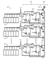
The input digital value can have any selected bit depth. Any type of DAC 610, voltage or current, can be used. In various aspects, since associative computing can be approximate in nature, a lower bit depth of the DAC can be used, or wider process variation permitted, than in prior schemes using non-associative comparison. Multiple rows are present, each driven by one DAC; the other rows are omitted for clarity. Memristors 130 connect row electrodes and column electrodes. Therefore the columns carry the dot products, as noted in FIG. 1 , as the current flowing out of each column. Resistors 610 represent the parasitic resistances of the row electrodes 110 (FIG. 1 ) and resistors 620 represent the parasitic resistances of the column electrodes 120 (FIG. 1 ).
Three spin neurons (DWNs) 300 are shown with their input (domain 301 terminals) connected to respective column lines of the RCN 100. A DC voltage, V, is applied to the domain 303 terminals of all the DWNs (access transistors are not shown for simplicity). Owing to the small resistance of the DWN devices, this effectively biases output ends of the RCN (connected to domain 301 terminals) to the same voltage. Each spin neuron 300 acts as a current-mode comparator. This is further discussed below with reference to FIG. 13 .
As a result, the current input through a memristor connecting the ith input bar to the jth output bar (in-plane) can be written as I(i,j)=ΔV·GT(i)GST/(GT(i)+GST)(G(i,j)/GST), where, G(i,j) is the programmed conductance of the memristor. For improved dot-product evaluation, the current I(i,j) can be proportional to the product of GT (i.e., the DTCS conductance, proportional to the input data) and G(i,j).
In various aspects, voltage signals are applied to the row electrodes 110 instead of currents. The applied voltage signals, e.g., the sources of drive transistors, can be connected to a voltage reference. The voltage reference can be selected with respect to the voltage on reference 503 of the DWNs 300 so that appropriate currents will be developed across memristors 130 and latched by latch circuits 500 (FIG. 5 ).
The range of current output from the DTCS-DAC needed can be selected based on the choice of WTA resolution. If the DWNs are designed to have a threshold of ˜1 μA, the maximum value of the dot-product output must be greater than 32 μA for a 5 bit resolution for the WTA. This in turn, translates to the required range of DAC output current. For 128-element input vectors and 5-bit resolution for the WTA, the maximum value for DAC output required can be ˜10 μA. This range of current can be obtained using different combination of DTCS sizing and the terminal voltage, ΔV. For a required amount of DAC current, ΔV can be reduced to reduce the static power consumption in the RCN. The minimum value of ΔV is limited mainly by the parasitic voltage drops that degrade the detection margin and hence the matching accuracy. For an example simulated design (RCN of size 128×40), a ΔV of 30 mV was found to be enough to preserve acceptable matching accuracy. Various aspects effectively bias the RCN across a small terminal voltage (ΔV), thereby ensures that the static current flow in RCN takes place across a small terminal voltage of ˜30 mV (between two DC supplies V and V+ΔV). As noted above, the application of DWN in the RCN offers the benefit of low voltage operation and reduces the static power consumption in a current-mode, analog computing mode.
When a plurality of dot products is available, e.g., as discussed above with reference to FIGS. 1 and 6 , it is desirable to determine which of the dot products is, e.g., the highest-magnitude, lowest-magnitude, most positive, or most negative of the dot products. A winner-take-all (WTA) circuit can be used for this purpose. WTA circuits can also be used for comparing data other than that provided by a memristor array.
A plurality of one-shots 1020 are connected to respective ones of the input stages 1010 to successively receive the bits of the respective code words therefrom. Each one-shot 1020 is configured to successively provide a first bit value, e.g., 1, until receiving a bit having a non-preferred value, e.g., 0, concurrently with an enable signal (“en”), and then to provide a second, different bit value, e.g., 0. To locate smaller values rather than larger, the non-preferred value can be 1. The first and second bit values can be interchanged with suitable changes to the circuit, e.g., adding inverters or changing the polarity of gate inputs or outputs.
An enable circuit 1030 is connected to the outputs of the one-shots 1020. The enable circuit 1030 is configured to provide the enable signal if at least one of the one-shots 1020 is providing the first bit value. Enable circuit 1030 can provide the enable signal by driving an output to a signal level corresponding to enabling. In this example, the enable signal is a high-logic-level output from the enable circuit 1030, and enables D flip-flops (DFFs) 1023, 1026 (for clarity, not all are labeled).
In the example shown, enable circuit 1030 includes a node 1032 selectively carrying the enable signal. The enable signal can have a different representation inside the enable circuit 1030 than outside. In this example, node 1032 carries a low logic level when enabled, and inverters 1034 (for clarity, not all are labeled) produce the desired high logic level to enable DFFs 1023, 1026. In another example, inverters 1034 or other components can be connected between enable circuit 1030 and one-shots 120.
Enable circuit 1030 also includes a precharge circuit 1036 configured to precharge the node 1032 to a signal level different from the enable signal, here a high logic level. The illustrated precharge circuit 1036 includes a pullup (e.g., a PFET) that pulls node 1032 to VDD (not providing the enable signal) when the PRECHG control input is low. Enable circuit 1030 in this example further includes a modification circuit 1038 (for clarity, not all are labeled) configured to provide the enable signal on the node 1032 in response to the first bit value from at least one of the one-shots. In this example, node 1032 is connected to a plurality of modification circuits 1038, each including a selective pulldown (e.g., an NFET) that pulls node 1032 to GND (providing the enable signal) whenever the output of a respective one-shot 1020 is outputting a high logic level. In this example, the enable signal corresponds to a low signal level of the node, and the signal level different from the enable signal corresponds to a high signal level of the node.
In the example shown, each of the one-shots 1020 includes an AND gate 1029 (for clarity, not all are labeled) and the first and second D flip-flops (DFFs) 1023, 1026 enabled by the enable signal. The output of the first DFF 1033 and the input of the first DFF 1033 are connected as the inputs of the AND gate 1029. The output of the AND gate 1029 is connected to the input of the second DFF 1026.
In this example, the input stages 1010 include output registers of successive-approximation (SAR) ADCs. Input data in SAR registers 1010 is provided to a chain of flip- flops 1023, 1026. As the number N of inputs increases, hardware size increases linearly (one input stage 1010 and one-shot 1020 per input). As bit width m increases, hardware size also grows only linearly (one bit in each SAR register and each DFF 1023, 1026 per input bit). The number of DFFs 1023, 1026 does not grow with m. In a simulated configuration, at m=6 the power consumption is similar to comparative schemes; for m>6, the power consumption of the inventive hardware is lower than the comparative hardware.
In various aspects, the WTA (including one-shots 1020 and enable circuit 1030) operates in parallel with a SAR ADC, the output registers of which are the registers in the input stage 1010. This system can be pipelined if desired. The WTA can also be used on digital bit-serial inputs, e.g., digitally-computed dot product or other correlation values.
The second half of the WTA algorithm can operate in parallel with the first (i.e., the ADC operation). In various aspects, results of the first ADC conversion step obtained from the SAR are directly transferred to tracking registers (DFFS 1023) through the pass-gate multiplexing switch (PGS). Thus that, at this stage, all the DFFs 1023 with a high output correspond to the ADC results with MSB=‘1’. In the second cycle operation, the detection line (node 1032) is first pre-charged to Vdd and the set of discharge registers (DFFs 1026), driving it are cleared to low output. Next, if for at least one of the SAR's with high MSB, the second MSB also evaluates to ‘1’, the corresponding DFF 1026 is driven high by the associated AND gate 1029. Thus, node 1032 is discharged to ground and the write of all the DFFs 1023 is enabled.
All the DFFs 1023 for which both, first and second MSB's evaluated to ‘1’, stay high, but the rest are set to low. In an example, if at least one of the SAR's (5-bit) evaluated to ‘11000’ in the second conversion cycle, node 1032 is discharged and DFFs 1023 with SAR value ‘11000’ stay high, while those with SAR value ‘10000’ are set to low. In case all SAR's evaluated to ‘10000’ in the second cycle, no change is made to the values in DFFs 1023. Thus, at the end of conversion cycle, if only one of the DFFs 1023 remains high-output, it is identified as the winner and the corresponding SAR value is effectively the degree of match (DOM).
The winner-tracking circuitry described above is fully digital and does not consume any static power (except for leakage). Moreover, each one-shot 1020 can use common control lines (“CTL”). This permits readily scaling with increases in N or m.
The overall power consumption in various aspects is drastically reduced as compared to a mixed-signal (MS) CMOS realization, due to two main reasons. Firstly, the power consumption in the RCN itself is significantly lowered due to low voltage operation, and secondly, the fully digital WTA structure avoids any additional static power consumption. Note that various WTA schemes implemented in MS-CMOS would result in large power consumption, resulting from conventional ADC's. The low-voltage current-mode switching characterisitics of DWN however, provides a compact and low power digitization technique. Various aspects herein can be implemented in a standard digital CMOS process.
In various aspects, each cycle, ones of the inputs that can be determined not to be the winner based on the current bit position i are deselected (On goes low). Input(s) that remain selected after all cycles are the winner or ties for the winner.
In various aspects the WTA operates in parallel with the SAR-ADC and hence operates on the successive bits of SAR-outputs. Referring to FIG. 12 and also to FIG. 11 , in this example, 3 inputs are provided, D1, D2, and D3, each of which is 4 bits wide (N=3, m=4). Two levels of multiplexers (1112, 1114) are shown at the input stage in FIG. 11 . The first stage (mux 1112) selects successive input bits of the data Dj, starting from the MSB. The second stage of multiplexers (mux 1114) conditionally passes the ith input bit of Dj (which is Dj(i)) in the ith cycle of WTA operation. Muxes 1114 are controlled by signals Cj which are same as the outputs of the corresponding WTA branch. In the first ADC conversion step, all Cj's are initialized to ‘1’ hence all Dj(m) (where m is the input bit-size) are directly transferred to the DFFs 1023 shown in FIG. 11 . The output of each DFF 1023 is also initialized to ‘1’ in the first cycle. Before each cycle, the Discharge Line (DL) shown in FIG. 11 is pre-charged to ‘1’. Thus, at the end of ith cycle the DL discharges if any one of the Oj's evaluate to ‘1’. For the example data-set given in FIG. 12 , this implies that in the first cycle all the outputs (Oi's) of the DFFs 1026 evaluate to ‘1’ and hence the DL is discharged. For the first cycle, all the MSB's were detected high, hence none of the three numbers Dj's can be rejected yet. Since all the outputs Oj's and hence the select lines Cj's are high after the first cycle, the 2nd bits of all the Dj's are selected by the stage-2 muxes and appear as the signals Pj. In the second cycle, O1 and O3 go high, however O2 evaluates to ‘0’ (since D1(2)=D3(2)=‘1’ but D3(2)=‘0’). The DL is again discharged. But for the next cycle, D2 is discarded from the WTA operation because of C2 turning low. As a result P2, and hence, O2, are clamped to ‘0’ for rest of the cycles. In the 3rd stage, both D1(3) and D2(3) are ‘0’ hence the DL fails to discharge. As a result all modifications in the DFFs 1023, 1026 and the muxes are disabled (using the ‘enable’ control shown in FIG. 11 ). In the 4th cycle, again, D1(4) and D3(4) are passed to the WTA. Note that the first and third DFFs 1023 are still storing ‘1’ as a result of the previous cycle evaluation; see Q1 and Q3. However, in the last cycle only O1 goes high (since D1(4)=‘1’ and D3(4)=‘0’), discharging DL. Hence, D3 is discarded from the WTA operation and D1 is identified as the winner, at end of the 4th cycle.
A fully parallel bit-serial digital Winner Take All (WTA) circuit according to various aspects described above can advantageously identify the largest among Nm-bit words in m cycles, even if N is a large number. The time taken by various WTA circuits herein to identify the maximum among the m-bit inputs is independent of the number of inputs N. This advantageously provides fast, low power WTA operation compared to prior schemes. Various WTAs herein can be combined with bit-serial data processing circuits such as bit-serial digital hardware for, e.g., Hamming-distance calculation or Successive Approximation Register Analog to Digital conversion (SAR-ADC); various of these combinations can be used in pattern matching hardware.
The operation of various WTAs herein is based on a new algorithm for detecting a winner among large number of parallel bit-serial inputs. The WTA can include a digital controller circuit and a digital logic block.
Various aspects can determine the highest of the N input values or the lowest, by interchanging 1 and 0 in the discussion above. In various aspects, a clock-driven pre-discharge circuit is operated by the logic and controller. An example WTA starts comparing Nm-bit inputs from the MSB position and proceeds towards the LSB in a total of m cycles. (Various aspects include one or more additional cycles for latency or pipelining, but the number of additional cycles does not vary with N.) In each cycle, any inputs determined to be smaller than the current maximum (e.g., any input with a 0 bit in the same position as a 1 bit in another input) (or larger, e.g., with a 1 bit where others have a 0 bit) are discarded from the comparison using the control and logic circuits. Inputs that are not clearly smaller (larger) than another input in the bit position under test are considered during subsequent stage(s) of comparison, where the next lower bit of significance, then the next, . . . , down to the LSB, is compared using the inventive charge-discharge circuit. The total process takes m+O(1) cycles for m-bit comparison and hence the total delay is independent of the number of WTA inputs N.
Each ADC 1320 includes input terminal 1330 and register 1310 connected to the respective input stage 1010 to successively provide the bits. Register 1310 can alternatively be part of input stage 1010.
In various aspects, the system also includes crossbar array 100 having a plurality of row electrodes 110, a plurality of column electrodes 120, and a plurality of resistive memory elements 130, each memory element 130 directly connected to one of the row electrodes 110 and one of the column electrodes 120; and a signal source 1342 configured to apply a plurality of test electrical signals to respective ones of the row electrodes 110. The column electrodes 120 are electrically connected to the input terminals of the respective ADCs 1320 in this example.
The “RCB network” is the column lines. Triangles are spin neurons. Outputs of neurons drive DTCS (binary-weighted) values. Value in SAR register is converted to a current by the DTCS, then compared to the dot product output. P is a Pass gate that modifies SAR value. E.g., if SAR is higher, reduce SAR.
The circuit realization of this operation using DWNs is shown in FIG. 13 . Output currents of the RCN columns (e.g., 40 columns storing the pattern vectors of 40 face-images; see FIGS. 20-21 ) are received by individual DWN input nodes that are effectively clamped at a DC supply V, as described earlier. Each DWN has an associated DTCS-DAC, which is driven by the corresponding successive approximation register 1310. The drain terminals of the DTCS transistors are a DC voltage V−ΔV. In each conversion cycle, the DWN device essentially compares the RCN output and the DAC output (and hence acts as the comparator of the SAR block). The comparison result is detected by the latch described in FIG. 5 , and the result is used to modify the register 1310 though pass-gate based multiplexers P, driven by controller 1386. In various aspects, the component of RCN output current sunk by the DTCS in the ADC's flow through across a DC level of 2ΔV. Note that for a neuron resistance of ˜50Ω, the current injection into it towards the final conversion steps (more MSB's) will be less than 5 μA (note, only the difference between DAC output and the dot-product output enters the neuron). This leads to a voltage drop of less than 0.3 mV.
The DWN device essentially acts as a low voltage, high speed, high resolution current-mode comparator and hence can be exploited in digitizing analog current levels at low energy cost. Various WTA techniques, algorithmically depicted in FIG. 14 , combine a digitization step with a parallel ‘winner-tracking’ operation.
The first half of the flowchart is an example algorithm for successive approximation register (SAR) ADC. To begin the conversion, the approximation register (that stores the digitization result) is initialized to the midscale (i.e., all but the most significant bit is set to 0). At every cycle a digital to analog converter (DAC) produces an analog level corresponding to the digital value stored in the SAR (step 1425) and a comparator compares it with the analog input using an analog comparator (step 1430, 1435). If the comparator output is high, the current bit remains high (step 1440), else it is turned low (step 1445) and the next lower bit is turned high. The process is repeated for all the bits. At the end of conversion, the SAR stores the digitized value corresponding to the analog input.
The second half of the WTA algorithm operates in parallel with the first (i.e., the ADC operation), as described above with reference to FIG. 10 . DFFs 1023 are referred to in the flowchart as “TR”; DFFs 1026 are “DR”; node 1032 is “DL”; register 1010 is “SAR”.
Simulations for MS-CMOS designs show that the power consumption for the WTA unit dominates the total power. On the other hand, for inventive techniques herein, there is negligible static power consumption in the WTA operation. However, since, the static power consumption in RCN is also significantly lowered, it becomes comparable to the dynamic switching power in the WTA. This is evident from the trend shown in FIG. 15 . It also shows that the static power consumption in the DWN-based design can be significantly reduced by lowering the DWN switching threshold further. However, the dynamic power remains almost constant and starts to dominate for reduced DWN thresholds.
In order to compare the performance of various aspects with state of the art mixed signal (MS) CMOS design, two different analog CMOS designs were simulated. These designed employed binary tree WTA circuits according to two prior schemes, using 45 nm CMOS technology models. The first design is the standard BT-WTA, whereas, the second is a recently proposed modification. A third 45 nm digital CMOS design was also simulated and employed multiply and accumulate operations for evaluating the correlation between the 5-bit 128 element digital templates and input features of the same size.
A micro-magnetic simulation model was used for DWN. The model that was calibrated with experimental data on DWMs. Effect of thermal fluctuation and device heating were also considered for characterizing the device. Behavioral model based on statistical characteristics of the device were used in SPICE simulation to assess the system level functionality. Some design parameters used are listed in Table 1.
| TABLE 1 |
| |
| Template |
| 16 × 8, | Magnet | NiFe | ||
| size | 5-bit | | ||
| # template | ||||
| 40 | free- |
3 × 33 × 60 nm3 | ||
| comparator | 5-bit | |
| resolution | Ms |
| 800 | emu/cm3 | |||||
| Input data | 100 | Ku2V | 20 | | ||
| rate | Ic | |||||
| 1 | μA | |||||
| crossbar | 1Ω/μm, | Tswitch | 1.5 | ns | ||
| parasitics | 0.4 fF/μm |
| Crossbar | Cu | Cross-bar | Cu | ||
| material | material | ||||
| memristor | Ag- | Resistance | 1 kΩ to 32 kΩ | ||
| material | range | ||||
The plot in FIG. 16 shows the impact of transistor process variations upon MS-CMOS designs. The power-delay products are plotted for a WTA resolution of 4%. Note that in an inventive WTA described herein, the impact of transistor-variations in the DTCS-DAC is limited to just a single step, whereas, the MS-CMOS circuits suffer more due to the cumulative effect of multiple transistors in the signal path. As discussed above, with larger variations, the accuracy and resolution of MS-CMOS circuits like current-mirrors decreases steeply, necessitating the use of larger devices, which impairs the circuit performance.
Table 2 compares a spin-CMOS design according to an aspect with prior MS-CMOS designs, and with the 45 nm digital CMOS design. The device parameters for the design used for Table 2 are given in Table 1. The results shown are for σVT=5 mV for minimum sized transistors. Results for three different WTA resolutions are given which show similar energy benefits of the inventive technique, even for smaller WTA resolution. Energy is given in relative units, and Table 2 compares power numbers and performance for the dot product operation and the WTA together. For analog designs, lower resolution constrain allows smaller transistors and hence better performance. Power consumption for the DWN based design, also reduces with resolution. Lower WTA resolution allows smaller DAC currents, resulting in reduced static power and lower switched capacitance for the smaller WTA blocks, leading to reduced dynamic power.
Results for comparison with 45 nm digital hardware shows ˜1000× lower computing energy for the inventive technique. Note that, this comparison does not include the overhead due to memory read in the digital design. As discussed earlier, digital hardware in general prove inefficient for the class of computation considered herein. Also, the use of MS-CMOS circuits in RCN barely perform ˜10× better than the digital implementation and hence achieve far less energy efficiency as compared to inventive designs herein. Thus, low-energy analog computing using spin neurons can significantly enhance the prospect of RCN technology for computational hardware.
| TABLE 2 |
| Performance |
| spin-CMOS | 45 nm Digital | |||
| PE | [18] | [17] | CMOS | |
| Power | 5-bit | 65 μW | 5.5 |
8 |
4 mW |
| 4-bit | 45 μW | 2.9 mW | 5.0 mW | 2.8 mW | |
| 3-bit | 32 μW | 2.3 mW | 3.2 mW | 1.2 |
| Frequency |
| 100 |
50 |
50 MHz | 2.5 MHz |
| Energy | 5- |
1 | 160 | 215 | 2460 |
| 4- |
1 | 140 | 221 | 2300 | |
| 3- |
1 | 155 | 210 | 1100 | |
Inventive designs herein can achieve more than three orders of magnitude lower energy cost as compared to a dedicated digital hardware. The use of spin-torque neurons can therefore boost the prospects of RCN as a computation tool.
In a crossbar array 100, comprising or consisting of large number of memristors 130, write voltage applied across two cross connected bars (one row 110, one column 120) for programming the interconnecting memristor 130 can also results in sneak current paths through neighboring devices. This can disturb the state of unselected memristors. To overcome the sneak path problem, application of access transistors and diodes can be used. Methods for programming one memristor 130 at a time without access transistors can also be used. In this example, row electrodes 1910 are connected to row switches 1910 and column electrodes 120 are connected to column switches 1920. As long as only one of the row switches 1910 and one of the column switches 1920 is closed at a time, only one memristor 130 will be programmed.
In order to accomplish the write operation, a constant current can be injected into the selected memristor 130 and the voltage developed on the row electrode 110 is compared with a comparator threshold by comparator 1930. The threshold, in turn, is set proportional to the target resistance, by using a compact switched capacitor digital to analog converter (DAC) 1940. The current source 1950 is disconnected as soon as the accessed memristor 130 acquires the target resistance value. A lower value of write current results in slower ramp in the resistance value and hence, allows more precise tuning. Various memristive devices (including Ag—Si) exhibit a finite write threshold for an applied current/voltage, below which there is negligible change in the resistance value. As described above, application of spin-based neurons in RCN facilitates ultra-low voltage (and hence low current) operation of the memristors 130 for computing and hence, can achieve reduced read-disturb for the array.
The write precision in the method described above is mainly limited by random offset of the comparator 1930 and inaccuracy in the current source 1950 and the DAC 1940.
In various examples, components shown in FIGS. 10, 13 and 19 are used together. Specifically, an electronic comparison system according to this example includes controller 1386 or another controller configured to automatically receive an input vector and a plurality of test vectors. Examples are discussed below with reference to FIGS. 20 and 21 . Controller 1386 operates writing circuit 1900 to store values from each of the test vectors in the resistive memory elements (memristors 130) directly connected to a respective one of the column electrodes 120. That is, each test vector runs down one column, as described above with reference to FIG. 1 . In aspects using nonvolatile resistive memory elements, the test vectors can be written once and used multiple times. Controller 1386 is further configured to operate the signal source 1342 to apply the test electrical signals corresponding to the input vector to the row electrodes 110. Controller 1386 is yet further configured to determine which one(s) of the test vectors satisfy a selected criterion with respect to the input vector using the outputs of the one-shots 1020 or another WTA circuit. In this way, complex pattern-matching and -searching tasks can be performed in a more power- and space-efficient way.
In a simulation, a resolution of 4% (5-bit) was chosen. Resolving ˜4% difference among the current-mode dot product results requires a precision of 5-bits for the detection unit, responsible for identifying the winning pattern. As described above with reference to FIG. 6 , in order to perform associative matching of an input face-image with the data stored in the RCN, each of the 128 digital values is converted into an analog voltage or current level, to be applied to the RCN row electrodes 110. For the data set of 400 individual images (with 40 mean templates stored in the array), a simulated WTA design of 5-bit resolution resulted in ˜93% matching accuracy.
The patterns are analog, so an RCN and WTA can be used to determine whether a test image of an input face image matches any of the patterns. The analog patterns are stored in resistive memory. Input patterns of current or voltage are applied on the rows and the dot products of the input and each stored vector are received on the columns as currents or voltages. The resulting analog vector of currents or voltages can be digitized using a spin neuron and a SAR ADC. A WTA circuit running in parallel can then determine the closest match.
Various aspects can be useful for pattern-matching hardware. Some aspects match stored patterns with input data and select the winner among a large number of stored patterns. WTA circuits herein can lead to low power and compact designs for such pattern-matching hardware, which is of great interest in the field of cognitive computing. A WTA herein can be fabricated in a standard CMOS process. Patterns do not have to be face images. In an example, if a random image is input to the hardware, various aspects will still identify the ‘winning’ pattern. But if the degree of match (DOM) is lower than a predetermined threshold, the winner can be discarded, implying that the input image does not belong to the stored data set.
The basic associative memory module (AMM) unit herein, including an RCN, SAR ADC, and WTA, can be extended. For example, very large number of images can be grouped into smaller clusters that can be hierarchically stored in the RCN modules. Individual patterns of larger dimensions can also be paritioned and stored in modular RCN blocks. Various aspects are applicable to a wide class of non-Boolean computing architectures that also include different categories of neural networks. For instance, the spin-RCN based correlation modules presented in this work can provide energy efficient hardware solution to convolutional neural networks that are attractive for cognitive computing tasks, but involve very high computational cost.
In various aspects, processor 2286 is configured to receive the respective stored bit values of the comparators 2230 from the latches 500. Processor 2286 determines updated weights using the selected weights stored in the memristors 130, the test electrical signals, and the received bit values. This can be done using known neural-network training algorithms such as those described in U.S. Pat. No. 8,694,451, incorporated herein by reference, or other supervised, unsupervised, or reinforcement algorithms, including but not limited to gradient-descent algorithms, particle-swarm optimization, genetic algorithms, evolutionary methods, simulated annealing, or expectation-maximization or other mathematical optimization methods. Processor 2286 then causes the writing circuit to store the updated weights in the resistive memory elements. In this way, the neural network can improve its performance on classification tasks.
Various aspects use analog rather than digital outputs. In these aspects, reference source 2216 includes a controller 1386 (FIG. 13 ) programmed to sequence through a selected number of bits, starting with a most-significant bit of the selected number of bits and a plurality of reference circuits, each configured to provide one of the reference electrical signal(s) to a respective one of the comparators. Each reference circuit includes a register 1310 configured to hold respective values for the selected number of bits; and a signal generator 1340 that provides the respective one of the reference electrical signals in response to the values in the register 1310. Each signal generator 1340 can include a binary-weighted transistor digital-to-analog converter (DAC) responsive to the values in the respective register 1310 to provide the respective one of the reference electrical signals.
The controller 1386 is configured to successively update the bits of each of the registers 1310 in the sequence according to the stored bit value in the respective one of the comparators 2230 (or 1350, FIG. 13 ). That is, the outputs of CMOS latches 500 are used by reference source 2216 to populate the registers 1310 with the digital representations of the analog values. Reference source 2216 changes VREF while controller 1386 cycles through the bits so that the values stored in the latches 500 are usable to successively approximate the analog values on the column lines 120 more and more accurately.
In various aspects, the reference source 2216 can then provide the digital values of registers 1310, e.g., N values, each with m bits, one for each column line 120, to processor 2286. Processor 2286 can then receive the respective bit values in the registers 1310, determine updated weights using the selected weights, the test electrical signals, and the received bit values, and cause the writing circuit 1900 to store the updated weights in the resistive memory elements 1300. In this way, processor 2286 can conduct neural network training as described above, but using analog outputs rather than digital. Processor 2286 can also use a combination of analog and digital outputs in neural-network training.
In view of the foregoing, various aspects provide lower-power, lower-area winner-take-all circuits and neural networks. A technical effect of various aspects is to receive input data and efficiently compare it to a set of known patterns.
The phrase “communicatively connected” includes any type of connection, wired or wireless, for communicating data between devices or processors. These devices or processors can be located in physical proximity or not. For example, subsystems such as peripheral system 2320, user interface system 2330, and data storage system 2340 are shown separately from the data processing system 2386 but can be stored completely or partially within the data processing system 2386.
The peripheral system 2320 can include one or more devices configured to provide digital content records to the processor 2386. For example, the peripheral system 2320 can include digital still cameras, digital video cameras, cellular phones, or other data processors. The processor 2386, upon receipt of digital content records from a device in the peripheral system 2320, can store such digital content records in the data storage system 2340.
The user interface system 2330 can convey information in either direction, or in both directions, between a user 2338 and the processor 2386 or other components of system 2301. The user interface system 2330 can include a mouse, a keyboard, another computer (connected, e.g., via a network or a null-modem cable), or any device or combination of devices from which data is input to the processor 2386. The user interface system 2330 also can include a display device, a processor-accessible memory, or any device or combination of devices to which data is output by the processor 2386. The user interface system 2330 and the data storage system 2340 can share a processor-accessible memory.
In various aspects, processor 2386 includes or is connected to communication interface 2315 that is coupled via network link 2316 (shown in phantom) to network 2350. For example, communication interface 2315 can include an integrated services digital network (ISDN) terminal adapter or a modem to communicate data via a telephone line; a network interface to communicate data via a local-area network (LAN), e.g., an Ethernet LAN, or wide-area network (WAN); or a radio to communicate data via a wireless link, e.g., WiFi or GSM. Communication interface 2315 sends and receives electrical, electromagnetic or optical signals that carry digital or analog data streams representing various types of information across network link 2316 to network 2350. Network link 2316 can be connected to network 2350 via a switch, gateway, hub, router, or other networking device.
In various aspects, system 2301 can communicate, e.g., via network 2350, with a data processing system 2302, which can include the same types of components as system 2301 but is not required to be identical thereto. Systems 2301, 2302 are communicatively connected via the network 2350. Each system 2301, 2302 executes computer program instructions to carry out methods or processes noted above.
In an example, data storage system 2340 includes code memory 2341, e.g., a RAM, and disk 2343, e.g., a tangible computer-readable rotational storage device such as a hard drive. Computer program instructions are read into code memory 2341 from disk 2343. Processor 2386 then executes one or more sequences of the computer program instructions loaded into code memory 2341, as a result performing process steps described herein. In this way, processor 2386 carries out a computer implemented process. For example, steps of methods described herein, blocks of the flowchart illustrations or block diagrams herein, and combinations of those, can be implemented by computer program instructions. Code memory 2341 can also store data, or can store only code.
Various aspects described herein may be embodied as systems or methods. Accordingly, various aspects herein may take the form of an entirely hardware aspect, an entirely software aspect (including firmware, resident software, micro-code, etc.), or an aspect combining software and hardware aspects These aspects can all generally be referred to herein as a “service,” “circuit,” “circuitry,” “module,” or “system.”
Furthermore, various aspects herein may be embodied as computer program products including computer readable program code stored on a tangible non-transitory computer readable medium. Such a medium can be manufactured as is conventional for such articles, e.g., by pressing a CD-ROM. The program code includes computer program instructions that can be loaded into processor 2386 (and possibly also other processors), to cause functions, acts, or operational steps of various aspects herein to be performed by the processor 2386 (or other processor). Computer program code for carrying out operations for various aspects described herein may be written in any combination of one or more programming language(s), and can be loaded from disk 2343 into code memory 2341 for execution. The program code may execute, e.g., entirely on processor 2386, partly on processor 2386 and partly on a remote computer connected to network 2350, or entirely on the remote computer.
The invention is inclusive of combinations of the aspects described herein. References to “a particular aspect” (or “embodiment” or “version”) and the like refer to features that are present in at least one aspect. Separate references to “an aspect” (or “embodiment”) or “particular aspects” or the like do not necessarily refer to the same aspect or aspects; however, such aspects are not mutually exclusive, unless so indicated or as are readily apparent to one of skill in the art. The use of singular or plural in referring to “method” or “methods” and the like is not limiting. The word “or” is used in this disclosure in a non-exclusive sense, unless otherwise explicitly noted.
Various aspects have been described in detail with particular reference to certain preferred aspects thereof, but it will be understood that variations, combinations, and modifications can be effected by a person of ordinary skill in the art within the spirit and scope of the invention
Claims (12)
1. An electronic comparison system, comprising:
a plurality of input stages, each configured to successively provide bits of a respective code word, starting with a most-significant bit thereof;
a plurality of one-shots connected to respective ones of the input stages to successively receive the bits of the respective code words, wherein each one-shot is configured to successively provide a first bit value until receiving a bit having a non-preferred value concurrently with an enable signal, and then to provide a second, different bit value;
an enable circuit connected to the outputs of the one-shots and configured to provide the enable signal if at least one of the one-shots is providing the first bit value.
2. The system according to claim 1 , wherein the enable circuit includes a node selectively carrying the enable signal, a precharge circuit configured to precharge the node to a signal level different from the enable signal, and a modification circuit configured to provide the enable signal on the node in response to the first bit value from at least one of the one-shots.
3. The system according to claim 2 , wherein the precharge circuit includes a pullup, the discharge circuit includes respective selective pulldowns controlled by the outputs of respective ones of the one-shots, the enable signal corresponds to a low signal level of the node, and the signal level different from the enable signal corresponds to a high signal level of the node.
4. The system according to claim 1 , wherein the non-preferred value is 0.
5. The system according to claim 4 , wherein the first bit value is 1 and the second, different bit value is 0.
6. The system according to claim 1 , wherein each of the one-shots includes an AND gate and first and second D flip-flops (DFFs) enabled by the enable signal, the output of the first DFF and the input of the first DFF are connected as the inputs of the AND gate, and the output of the AND gate is connected to the input of the second DFF.
7. The system according to claim 6 , further including a gate configured to force the input of the first DFF to the non-preferred value if the output of the second DFF is the second, different bit value and the enable signal is provided.
8. The system according to claim 1 , further comprising a controller programmed to sequence through a selected number of bits and a plurality of successive-approximation analog-to-digital converters (ADCs), wherein the each input stage successively receives the bits from a respective one of the ADCs and each ADC comprises:
an input terminal;
a register connected to the respective input stage to successively provide the bits;
a programmable reference that provides a reference electrical signal in response to the value in the register; and
a comparator configured to compare an electrical signal at the input terminal to the reference electrical signal and adjust a bit in the register indicated by the controller, wherein the comparator includes a domain-wall neuron connected to the input terminal and the programmable reference and a CMOS latch configured to compare an output of the domain-wall neuron with a selected threshold and store a bit value according to the result of the comparison.
9. The system according to claim 8 , wherein the programmable reference includes a binary-weighted transistor digital-to-analog converter (DAC) responsive to the value in the register to provide the reference electrical signal.
10. The system according to claim 8 , further including:
a crossbar array having a plurality of row electrodes, a plurality of column electrodes, and a plurality of resistive memory elements, each memory element directly connected to one of the row electrodes and one of the column electrodes; and
a signal source configured to apply a plurality of test electrical signals to respective ones of the row electrodes;
wherein the column electrodes are electrically connected to the input terminals of the respective ADCs.
11. The system according to claim 10 , further including a writing circuit configured to store selected values in the resistive memory elements.
12. The system according to claim 11 , further including a controller configured to automatically:
receive an input vector and a plurality of test vectors;
operate the writing circuit to store values from each of the test vectors in the resistive memory elements directly connected to a respective one of the column electrodes;
operate the signal source to apply the test electrical signals corresponding to the input vector;
determine which one(s) of the test vectors satisfy a selected criterion with respect to the input vector using the outputs of the one-shots.
Priority Applications (2)
| Application Number | Priority Date | Filing Date | Title |
|---|---|---|---|
| US15/334,649 US9813048B2 (en) | 2014-05-27 | 2016-10-26 | Electronic comparison systems |
| US15/801,535 US10476487B2 (en) | 2014-05-27 | 2017-11-02 | Electronic comparison systems |
Applications Claiming Priority (2)
| Application Number | Priority Date | Filing Date | Title |
|---|---|---|---|
| US14/287,701 US9489618B2 (en) | 2014-05-27 | 2014-05-27 | Electronic comparison systems |
| US15/334,649 US9813048B2 (en) | 2014-05-27 | 2016-10-26 | Electronic comparison systems |
Related Parent Applications (1)
| Application Number | Title | Priority Date | Filing Date |
|---|---|---|---|
| US14/287,701 Division US9489618B2 (en) | 2014-05-27 | 2014-05-27 | Electronic comparison systems |
Related Child Applications (1)
| Application Number | Title | Priority Date | Filing Date |
|---|---|---|---|
| US15/801,535 Continuation US10476487B2 (en) | 2014-05-27 | 2017-11-02 | Electronic comparison systems |
Publications (2)
| Publication Number | Publication Date |
|---|---|
| US20170047913A1 US20170047913A1 (en) | 2017-02-16 |
| US9813048B2 true US9813048B2 (en) | 2017-11-07 |
Family
ID=54702187
Family Applications (3)
| Application Number | Title | Priority Date | Filing Date |
|---|---|---|---|
| US14/287,701 Active US9489618B2 (en) | 2014-05-27 | 2014-05-27 | Electronic comparison systems |
| US15/334,649 Active US9813048B2 (en) | 2014-05-27 | 2016-10-26 | Electronic comparison systems |
| US15/801,535 Active US10476487B2 (en) | 2014-05-27 | 2017-11-02 | Electronic comparison systems |
Family Applications Before (1)
| Application Number | Title | Priority Date | Filing Date |
|---|---|---|---|
| US14/287,701 Active US9489618B2 (en) | 2014-05-27 | 2014-05-27 | Electronic comparison systems |
Family Applications After (1)
| Application Number | Title | Priority Date | Filing Date |
|---|---|---|---|
| US15/801,535 Active US10476487B2 (en) | 2014-05-27 | 2017-11-02 | Electronic comparison systems |
Country Status (1)
| Country | Link |
|---|---|
| US (3) | US9489618B2 (en) |
Cited By (2)
| Publication number | Priority date | Publication date | Assignee | Title |
|---|---|---|---|---|
| US10726331B1 (en) | 2019-08-26 | 2020-07-28 | International Business Machines Corporation | Neural network circuits providing early integration before analog-to-digital conversion |
| US11038520B1 (en) * | 2020-04-15 | 2021-06-15 | International Business Machines Corporation | Analog-to-digital conversion with reconfigurable function mapping for neural networks activation function acceleration |
Families Citing this family (46)
| Publication number | Priority date | Publication date | Assignee | Title |
|---|---|---|---|---|
| CN106463166A (en) * | 2014-04-30 | 2017-02-22 | 慧与发展有限责任合伙企业 | Regulating memristor switching pulses |
| US9489618B2 (en) | 2014-05-27 | 2016-11-08 | Purdue Research Foudation | Electronic comparison systems |
| US10242313B2 (en) * | 2014-07-18 | 2019-03-26 | James LaRue | Joint proximity association template for neural networks |
| US10109348B2 (en) * | 2014-10-30 | 2018-10-23 | Hewlett Packard Enterprise Development Lp | Double bias memristive dot product engine for vector processing |
| US10347352B2 (en) * | 2015-04-29 | 2019-07-09 | Hewlett Packard Enterprise Development Lp | Discrete-time analog filtering |
| US9934463B2 (en) * | 2015-05-15 | 2018-04-03 | Arizona Board Of Regents On Behalf Of Arizona State University | Neuromorphic computational system(s) using resistive synaptic devices |
| EP3304557B1 (en) * | 2015-06-05 | 2023-12-13 | King Abdullah University Of Science And Technology | Resistive content addressable memory based in-memory computation architecture |
| US10191666B1 (en) * | 2015-08-25 | 2019-01-29 | Adesto Technologies Corporation | Write parameter switching in a memory device |
| US11579677B2 (en) * | 2015-12-18 | 2023-02-14 | Hewlett Packard Enterprise Development Lp | Memristor crossbar arrays to activate processors |
| WO2017131792A1 (en) * | 2016-01-30 | 2017-08-03 | Hewlett Packard Enterprise Development Lp | Dot product engine with negation indicator |
| EP3414702A1 (en) * | 2016-02-08 | 2018-12-19 | Spero Devices, Inc. | Analog co-processor |
| US10529418B2 (en) | 2016-02-19 | 2020-01-07 | Hewlett Packard Enterprise Development Lp | Linear transformation accelerators |
| US10332592B2 (en) * | 2016-03-11 | 2019-06-25 | Hewlett Packard Enterprise Development Lp | Hardware accelerators for calculating node values of neural networks |
| EP3286639A4 (en) | 2016-03-31 | 2018-03-28 | Hewlett-Packard Enterprise Development LP | Assigning data to a resistive memory array based on a significance level |
| US11741352B2 (en) | 2016-08-22 | 2023-08-29 | International Business Machines Corporation | Area and power efficient implementation of resistive processing units using complementary metal oxide semiconductor technology |
| US10089574B2 (en) * | 2016-09-14 | 2018-10-02 | Hewlett Packard Enterprise Development Lp | Neuron circuits |
| US10786171B2 (en) * | 2016-10-25 | 2020-09-29 | Hewlett-Packard Development Company, L.P. | Memristor code comparator to compare sensor signals to reference signals |
| WO2018112736A1 (en) * | 2016-12-20 | 2018-06-28 | 北京大学 | Data search system and method |
| US11304140B2 (en) * | 2017-01-31 | 2022-04-12 | Hewlett-Packard Development Company, L.P. | Memristor code comparator to compare wake up signals to reference signals |
| US11315009B2 (en) * | 2017-03-03 | 2022-04-26 | Hewlett Packard Enterprise Development Lp | Analog multiplier-accumulators |
| US10553299B2 (en) | 2017-04-14 | 2020-02-04 | Tdk Corporation | Magnetic domain wall type analog memory element, magnetic domain wall type analog memory, nonvolatile logic circuit, and magnetic neuro-element |
| WO2018189964A1 (en) | 2017-04-14 | 2018-10-18 | Tdk株式会社 | Magnetic domain wall utilizing analog memory element, magnetic domain wall utilizing analog memory, non-volatile logic circuit and magnetic neuro-element |
| US10055383B1 (en) | 2017-04-28 | 2018-08-21 | Hewlett Packard Enterprise Development Lp | Matrix circuits |
| US11169732B2 (en) | 2017-05-18 | 2021-11-09 | Kabushiki Kaisha Toshiba | Computing device |
| US11348002B2 (en) | 2017-10-24 | 2022-05-31 | International Business Machines Corporation | Training of artificial neural networks |
| US10739186B2 (en) | 2017-11-20 | 2020-08-11 | Samsung Electronics Co., Ltd. | Bi-directional weight cell |
| WO2019212488A1 (en) * | 2018-04-30 | 2019-11-07 | Hewlett Packard Enterprise Development Lp | Acceleration of model/weight programming in memristor crossbar arrays |
| US11177432B2 (en) | 2018-06-07 | 2021-11-16 | International Business Machines Corporation | Heusler-alloy and ferrimagnet based magnetic domain-wall devices for artificial neural network applications |
| US10224949B1 (en) * | 2018-07-26 | 2019-03-05 | Synaptics Incorporated | Shared cycle LSB generation for an array of successive approximation analog-to-digital converters |
| US10591541B2 (en) * | 2018-08-13 | 2020-03-17 | Micron Technology, Inc. | Comparator |
| CN109344967B (en) * | 2018-08-31 | 2021-09-14 | 武汉大学 | Intelligent electric meter life cycle prediction method based on artificial neural network |
| CN109710973B (en) * | 2018-11-22 | 2023-02-10 | 温州大学 | Method for optimizing area, power consumption and time delay of three-value fixed polarity RM circuit |
| CN109800870B (en) * | 2019-01-10 | 2020-09-18 | 华中科技大学 | Neural network online learning system based on memristor |
| US11386320B2 (en) * | 2019-03-06 | 2022-07-12 | International Business Machines Corporation | Magnetic domain wall-based non-volatile, linear and bi-directional synaptic weight element |
| US11145339B2 (en) | 2019-05-31 | 2021-10-12 | Taiwan Semiconductor Manufacturing Company, Ltd. | Device and method for computing-in-memory |
| CN110334799B (en) * | 2019-07-12 | 2022-05-24 | 电子科技大学 | Neural network reasoning and training accelerator based on storage and calculation integration and operation method thereof |
| US10915248B1 (en) | 2019-08-07 | 2021-02-09 | Macronix International Co., Ltd. | Memory device |
| CN110572149B (en) * | 2019-08-09 | 2021-06-11 | 华中科技大学 | Toffoli gate circuit and operation method thereof |
| CN110797067B (en) * | 2019-10-21 | 2021-10-22 | 上海闪易半导体有限公司 | Storage array module and control method, device and module thereof |
| CN112862663B (en) * | 2019-11-12 | 2023-06-16 | 芜湖每刻深思智能科技有限公司 | Near sensor end computing system |
| US11539370B2 (en) * | 2020-02-23 | 2022-12-27 | Tetramem Inc. | Analog to analog quantizer in crossbar array circuits for in-memory computing |
| CN111291879B (en) * | 2020-03-29 | 2023-08-22 | 湖南大学 | Signal generating device with habit and sensitization |
| US11443171B2 (en) | 2020-07-15 | 2022-09-13 | International Business Machines Corporation | Pulse generation for updating crossbar arrays |
| US11568217B2 (en) | 2020-07-15 | 2023-01-31 | International Business Machines Corporation | Sparse modifiable bit length deterministic pulse generation for updating analog crossbar arrays |
| CN112885963B (en) * | 2021-01-13 | 2022-12-09 | 西安交通大学 | Memristor cross array |
| US11735281B2 (en) * | 2021-04-30 | 2023-08-22 | Hewlett Packard Enterprise Development Lp | Analog content addressable memory with analog input and analog output |
Citations (29)
| Publication number | Priority date | Publication date | Assignee | Title |
|---|---|---|---|---|
| US3577084A (en) * | 1969-11-03 | 1971-05-04 | Singer General Precision | Computer sound generator |
| US3638196A (en) * | 1969-07-14 | 1972-01-25 | Matsushita Electric Ind Co Ltd | Learning machine |
| US3675204A (en) * | 1970-05-04 | 1972-07-04 | Varian Associates | Status system |
| US3882303A (en) * | 1974-04-08 | 1975-05-06 | Us Navy | Digital frequency correlator |
| US3967061A (en) * | 1975-03-05 | 1976-06-29 | Ncr Corporation | Method and apparatus for recovering data and clock information in a self-clocking data stream |
| US3970989A (en) * | 1974-03-06 | 1976-07-20 | Ontel Corporation | Data transfer error check |
| US4631670A (en) * | 1984-07-11 | 1986-12-23 | Ibm Corporation | Interrupt level sharing |
| US4843263A (en) * | 1986-01-10 | 1989-06-27 | Nec Corporation | Clock timing controller for a plurality of LSI chips |
| US4864543A (en) * | 1987-04-30 | 1989-09-05 | Texas Instruments Incorporated | First-in, first-out memory with counter address pointers for generating multiple memory status flags |
| US5165009A (en) * | 1990-01-24 | 1992-11-17 | Hitachi, Ltd. | Neural network processing system using semiconductor memories |
| US5336937A (en) * | 1992-08-28 | 1994-08-09 | State University Of New York | Programmable analog synapse and neural networks incorporating same |
| US5450621A (en) * | 1992-08-18 | 1995-09-12 | U.S. Philips Corporation | Radio receiver with digital control loop for coarse frequency acquisition and analog control loop for frequency lock-in |
| US5479579A (en) * | 1992-09-04 | 1995-12-26 | The United States Of America As Represented By The Administrator Of The National Aeronautics And Space Administration | Cascaded VLSI neural network architecture for on-line learning |
| US5542051A (en) * | 1993-03-03 | 1996-07-30 | Mitsubishi Denki Kabushiki Kaisha | Watch dog timer |
| US5588090A (en) * | 1993-05-20 | 1996-12-24 | Ricoh Company, Ltd. | Signal processing apparatus |
| US5588069A (en) * | 1990-12-19 | 1996-12-24 | Canon Kabushiki Kaisha | Image processing apparatus for advantageously encoding blocks of data having either substantially the same or varied colors |
| US6389404B1 (en) * | 1998-12-30 | 2002-05-14 | Irvine Sensors Corporation | Neural processing module with input architectures that make maximal use of a weighted synapse array |
| US20040039717A1 (en) * | 2002-08-22 | 2004-02-26 | Alex Nugent | High-density synapse chip using nanoparticles |
| US6844582B2 (en) * | 2002-05-10 | 2005-01-18 | Matsushita Electric Industrial Co., Ltd. | Semiconductor device and learning method thereof |
| US20060123280A1 (en) | 2004-11-17 | 2006-06-08 | Tran Hieu V | Test circuit and method for multilevel cell flash memory |
| US7085749B2 (en) * | 2001-05-31 | 2006-08-01 | Canon Kabushiki Kaisha | Pulse signal circuit, parallel processing circuit, pattern recognition system, and image input system |
| US7577020B2 (en) * | 2007-10-01 | 2009-08-18 | Shine Chung | System and method for reading multiple magnetic tunnel junctions with a single select transistor |
| US20100241601A1 (en) * | 2009-03-20 | 2010-09-23 | Irvine Sensors Corporation | Apparatus comprising artificial neuronal assembly |
| US20100238700A1 (en) * | 2009-03-17 | 2010-09-23 | Seagate Technology Llc | Quiescent Testing of Non-Volatile Memory Array |
| US20130132314A1 (en) * | 2010-07-30 | 2013-05-23 | Hewlett-Packard Development Company, L.P. | Systems and methods for modeling binary synapses |
| US20130285739A1 (en) * | 2010-09-07 | 2013-10-31 | Corporation De L ' Ecole Polytechnique De Montreal | Methods, apparatus and system to support large-scale micro- systems including embedded and distributed power supply, thermal regulation, multi-distributedsensors and electrical signal propagation |
| US20140028347A1 (en) * | 2012-07-30 | 2014-01-30 | Warren Robinett | Implementing logic circuits with memristors |
| US8923040B2 (en) * | 2013-01-30 | 2014-12-30 | Taiwan Semiconductor Manufacturing Co., Ltd. | Accommodating balance of bit line and source line resistances in magnetoresistive random access memory |
| US20150347896A1 (en) | 2014-05-27 | 2015-12-03 | Purdue Research Foundation | Electronic comparison systems |
Family Cites Families (3)
| Publication number | Priority date | Publication date | Assignee | Title |
|---|---|---|---|---|
| US3757226A (en) * | 1972-01-17 | 1973-09-04 | Collins Radio Co | Orse code type signals digital means for improving the signal to noise ratio of repetitive m |
| JPS59171387A (en) * | 1983-03-18 | 1984-09-27 | Hitachi Ltd | Method for constituting television signal |
| US10095718B2 (en) * | 2013-10-16 | 2018-10-09 | University Of Tennessee Research Foundation | Method and apparatus for constructing a dynamic adaptive neural network array (DANNA) |
-
2014
- 2014-05-27 US US14/287,701 patent/US9489618B2/en active Active
-
2016
- 2016-10-26 US US15/334,649 patent/US9813048B2/en active Active
-
2017
- 2017-11-02 US US15/801,535 patent/US10476487B2/en active Active
Patent Citations (29)
| Publication number | Priority date | Publication date | Assignee | Title |
|---|---|---|---|---|
| US3638196A (en) * | 1969-07-14 | 1972-01-25 | Matsushita Electric Ind Co Ltd | Learning machine |
| US3577084A (en) * | 1969-11-03 | 1971-05-04 | Singer General Precision | Computer sound generator |
| US3675204A (en) * | 1970-05-04 | 1972-07-04 | Varian Associates | Status system |
| US3970989A (en) * | 1974-03-06 | 1976-07-20 | Ontel Corporation | Data transfer error check |
| US3882303A (en) * | 1974-04-08 | 1975-05-06 | Us Navy | Digital frequency correlator |
| US3967061A (en) * | 1975-03-05 | 1976-06-29 | Ncr Corporation | Method and apparatus for recovering data and clock information in a self-clocking data stream |
| US4631670A (en) * | 1984-07-11 | 1986-12-23 | Ibm Corporation | Interrupt level sharing |
| US4843263A (en) * | 1986-01-10 | 1989-06-27 | Nec Corporation | Clock timing controller for a plurality of LSI chips |
| US4864543A (en) * | 1987-04-30 | 1989-09-05 | Texas Instruments Incorporated | First-in, first-out memory with counter address pointers for generating multiple memory status flags |
| US5165009A (en) * | 1990-01-24 | 1992-11-17 | Hitachi, Ltd. | Neural network processing system using semiconductor memories |
| US5588069A (en) * | 1990-12-19 | 1996-12-24 | Canon Kabushiki Kaisha | Image processing apparatus for advantageously encoding blocks of data having either substantially the same or varied colors |
| US5450621A (en) * | 1992-08-18 | 1995-09-12 | U.S. Philips Corporation | Radio receiver with digital control loop for coarse frequency acquisition and analog control loop for frequency lock-in |
| US5336937A (en) * | 1992-08-28 | 1994-08-09 | State University Of New York | Programmable analog synapse and neural networks incorporating same |
| US5479579A (en) * | 1992-09-04 | 1995-12-26 | The United States Of America As Represented By The Administrator Of The National Aeronautics And Space Administration | Cascaded VLSI neural network architecture for on-line learning |
| US5542051A (en) * | 1993-03-03 | 1996-07-30 | Mitsubishi Denki Kabushiki Kaisha | Watch dog timer |
| US5588090A (en) * | 1993-05-20 | 1996-12-24 | Ricoh Company, Ltd. | Signal processing apparatus |
| US6389404B1 (en) * | 1998-12-30 | 2002-05-14 | Irvine Sensors Corporation | Neural processing module with input architectures that make maximal use of a weighted synapse array |
| US7085749B2 (en) * | 2001-05-31 | 2006-08-01 | Canon Kabushiki Kaisha | Pulse signal circuit, parallel processing circuit, pattern recognition system, and image input system |
| US6844582B2 (en) * | 2002-05-10 | 2005-01-18 | Matsushita Electric Industrial Co., Ltd. | Semiconductor device and learning method thereof |
| US20040039717A1 (en) * | 2002-08-22 | 2004-02-26 | Alex Nugent | High-density synapse chip using nanoparticles |
| US20060123280A1 (en) | 2004-11-17 | 2006-06-08 | Tran Hieu V | Test circuit and method for multilevel cell flash memory |
| US7577020B2 (en) * | 2007-10-01 | 2009-08-18 | Shine Chung | System and method for reading multiple magnetic tunnel junctions with a single select transistor |
| US20100238700A1 (en) * | 2009-03-17 | 2010-09-23 | Seagate Technology Llc | Quiescent Testing of Non-Volatile Memory Array |
| US20100241601A1 (en) * | 2009-03-20 | 2010-09-23 | Irvine Sensors Corporation | Apparatus comprising artificial neuronal assembly |
| US20130132314A1 (en) * | 2010-07-30 | 2013-05-23 | Hewlett-Packard Development Company, L.P. | Systems and methods for modeling binary synapses |
| US20130285739A1 (en) * | 2010-09-07 | 2013-10-31 | Corporation De L ' Ecole Polytechnique De Montreal | Methods, apparatus and system to support large-scale micro- systems including embedded and distributed power supply, thermal regulation, multi-distributedsensors and electrical signal propagation |
| US20140028347A1 (en) * | 2012-07-30 | 2014-01-30 | Warren Robinett | Implementing logic circuits with memristors |
| US8923040B2 (en) * | 2013-01-30 | 2014-12-30 | Taiwan Semiconductor Manufacturing Co., Ltd. | Accommodating balance of bit line and source line resistances in magnetoresistive random access memory |
| US20150347896A1 (en) | 2014-05-27 | 2015-12-03 | Purdue Research Foundation | Electronic comparison systems |
Non-Patent Citations (3)
| Title |
|---|
| Office Action for U.S. Appl. No. 14/287,701, dated Dec. 17, 2015, Roy et al., "Electronic Comparison Systems", 9 pages. |
| Office Action for U.S. Appl. No. 14/287,701, dated Jul. 12, 2016, Roy, "Electronic Comparison Systems", 9 pages. |
| Sharad et al., "Spin-Based Neuron Model with Domain-Wall Magnets as Synapse", IEEE Transactions on Nanotechnology, vol. 11, No. 4, 2012, 11 pages. |
Cited By (2)
| Publication number | Priority date | Publication date | Assignee | Title |
|---|---|---|---|---|
| US10726331B1 (en) | 2019-08-26 | 2020-07-28 | International Business Machines Corporation | Neural network circuits providing early integration before analog-to-digital conversion |
| US11038520B1 (en) * | 2020-04-15 | 2021-06-15 | International Business Machines Corporation | Analog-to-digital conversion with reconfigurable function mapping for neural networks activation function acceleration |
Also Published As
| Publication number | Publication date |
|---|---|
| US10476487B2 (en) | 2019-11-12 |
| US20150347896A1 (en) | 2015-12-03 |
| US20180069536A1 (en) | 2018-03-08 |
| US9489618B2 (en) | 2016-11-08 |
| US20170047913A1 (en) | 2017-02-16 |
Similar Documents
| Publication | Publication Date | Title |
|---|---|---|
| US10476487B2 (en) | Electronic comparison systems | |
| Sharad et al. | Energy-efficient non-Boolean computing with spin neurons and resistive memory | |
| Sharad et al. | Ultra low power associative computing with spin neurons and resistive crossbar memory | |
| Fan et al. | Hierarchical temporal memory based on spin-neurons and resistive memory for energy-efficient brain-inspired computing | |
| Xue et al. | Embedded 1-Mb ReRAM-based computing-in-memory macro with multibit input and weight for CNN-based AI edge processors | |
| Daniels et al. | Energy-efficient stochastic computing with superparamagnetic tunnel junctions | |
| Sengupta et al. | Probabilistic deep spiking neural systems enabled by magnetic tunnel junction | |
| Kaiser et al. | Hardware-aware in situ learning based on stochastic magnetic tunnel junctions | |
| US20230113231A1 (en) | Methods and systems of operating a neural circuit in a non-volatile memory based neural-array | |
| Liu et al. | A memristor crossbar based computing engine optimized for high speed and accuracy | |
| Shreya et al. | Energy-efficient all-spin BNN using voltage-controlled spin-orbit torque device for digit recognition | |
| US20210174182A1 (en) | Mtj-based hardware synapse implementation for binary and ternary deep neural networks | |
| US20230297235A1 (en) | Sram-based cell for in-memory computing and hybrid computations/storage memory architecture | |
| Huang et al. | Fefet based in-memory hyperdimensional encoding design | |
| Zanotti et al. | Low-Bit precision neural network architecture with high immunity to variability and random telegraph noise based on resistive memories | |
| Scott et al. | A flash-based current-mode IC to realize quantized neural networks | |
| Yang et al. | Matching in memristor based auto-associative memory with application to pattern recognition | |
| Sharad et al. | Ultra-low power neuromorphic computing with spin-torque devices | |
| Scott et al. | An extremely low-voltage floating gate artificial neuron | |
| Xu et al. | A hybrid precision low power computing-in-memory architecture for neural networks | |
| Fida et al. | An active memristor based rate-coded spiking neural network | |
| TWI795766B (en) | Computing system, computing device and computing method | |
| Chen et al. | A Low-Cost Training Method of ReRAM Inference Accelerator Chips for Binarized Neural Networks to Recover Accuracy Degradation due to Statistical Variabilities | |
| US20230177319A1 (en) | Methods and systems of operating a neural circuit in a non-volatile memory based neural-array | |
| Reidy et al. | SOT-MRAM based Sigmoidal Neuron for Neuromorphic Architectures |
Legal Events
| Date | Code | Title | Description |
|---|---|---|---|
| STCF | Information on status: patent grant |
Free format text: PATENTED CASE |
|
| MAFP | Maintenance fee payment |
Free format text: PAYMENT OF MAINTENANCE FEE, 4TH YEAR, LARGE ENTITY (ORIGINAL EVENT CODE: M1551); ENTITY STATUS OF PATENT OWNER: LARGE ENTITY Year of fee payment: 4 |