WO2016079902A1 - Dual band multi-layer dipole antennas for wireless electronic devices - Google Patents
Dual band multi-layer dipole antennas for wireless electronic devices Download PDFInfo
- Publication number
- WO2016079902A1 WO2016079902A1 PCT/JP2015/002548 JP2015002548W WO2016079902A1 WO 2016079902 A1 WO2016079902 A1 WO 2016079902A1 JP 2015002548 W JP2015002548 W JP 2015002548W WO 2016079902 A1 WO2016079902 A1 WO 2016079902A1
- Authority
- WO
- WIPO (PCT)
- Prior art keywords
- electronic device
- wireless electronic
- dipole antenna
- highband
- lowband
- Prior art date
Links
Images


Classifications
-
- H—ELECTRICITY
- H01—ELECTRIC ELEMENTS
- H01Q—ANTENNAS, i.e. RADIO AERIALS
- H01Q21/00—Antenna arrays or systems
- H01Q21/06—Arrays of individually energised antenna units similarly polarised and spaced apart
- H01Q21/20—Arrays of individually energised antenna units similarly polarised and spaced apart the units being spaced along or adjacent to a curvilinear path
-
- H—ELECTRICITY
- H01—ELECTRIC ELEMENTS
- H01Q—ANTENNAS, i.e. RADIO AERIALS
- H01Q9/00—Electrically-short antennas having dimensions not more than twice the operating wavelength and consisting of conductive active radiating elements
- H01Q9/04—Resonant antennas
- H01Q9/16—Resonant antennas with feed intermediate between the extremities of the antenna, e.g. centre-fed dipole
- H01Q9/28—Conical, cylindrical, cage, strip, gauze, or like elements having an extended radiating surface; Elements comprising two conical surfaces having collinear axes and adjacent apices and fed by two-conductor transmission lines
- H01Q9/285—Planar dipole
-
- G—PHYSICS
- G06—COMPUTING; CALCULATING OR COUNTING
- G06Q—INFORMATION AND COMMUNICATION TECHNOLOGY [ICT] SPECIALLY ADAPTED FOR ADMINISTRATIVE, COMMERCIAL, FINANCIAL, MANAGERIAL OR SUPERVISORY PURPOSES; SYSTEMS OR METHODS SPECIALLY ADAPTED FOR ADMINISTRATIVE, COMMERCIAL, FINANCIAL, MANAGERIAL OR SUPERVISORY PURPOSES, NOT OTHERWISE PROVIDED FOR
- G06Q30/00—Commerce
- G06Q30/02—Marketing; Price estimation or determination; Fundraising
- G06Q30/0201—Market modelling; Market analysis; Collecting market data
- G06Q30/0206—Price or cost determination based on market factors
-
- G—PHYSICS
- G06—COMPUTING; CALCULATING OR COUNTING
- G06Q—INFORMATION AND COMMUNICATION TECHNOLOGY [ICT] SPECIALLY ADAPTED FOR ADMINISTRATIVE, COMMERCIAL, FINANCIAL, MANAGERIAL OR SUPERVISORY PURPOSES; SYSTEMS OR METHODS SPECIALLY ADAPTED FOR ADMINISTRATIVE, COMMERCIAL, FINANCIAL, MANAGERIAL OR SUPERVISORY PURPOSES, NOT OTHERWISE PROVIDED FOR
- G06Q30/00—Commerce
- G06Q30/02—Marketing; Price estimation or determination; Fundraising
- G06Q30/0207—Discounts or incentives, e.g. coupons or rebates
-
- H—ELECTRICITY
- H01—ELECTRIC ELEMENTS
- H01Q—ANTENNAS, i.e. RADIO AERIALS
- H01Q21/00—Antenna arrays or systems
- H01Q21/0006—Particular feeding systems
- H01Q21/0075—Stripline fed arrays
-
- H—ELECTRICITY
- H01—ELECTRIC ELEMENTS
- H01Q—ANTENNAS, i.e. RADIO AERIALS
- H01Q21/00—Antenna arrays or systems
- H01Q21/30—Combinations of separate antenna units operating in different wavebands and connected to a common feeder system
-
- H—ELECTRICITY
- H01—ELECTRIC ELEMENTS
- H01Q—ANTENNAS, i.e. RADIO AERIALS
- H01Q5/00—Arrangements for simultaneous operation of antennas on two or more different wavebands, e.g. dual-band or multi-band arrangements
- H01Q5/40—Imbricated or interleaved structures; Combined or electromagnetically coupled arrangements, e.g. comprising two or more non-connected fed radiating elements
- H01Q5/48—Combinations of two or more dipole type antennas
-
- H—ELECTRICITY
- H01—ELECTRIC ELEMENTS
- H01Q—ANTENNAS, i.e. RADIO AERIALS
- H01Q9/00—Electrically-short antennas having dimensions not more than twice the operating wavelength and consisting of conductive active radiating elements
- H01Q9/04—Resonant antennas
- H01Q9/06—Details
- H01Q9/065—Microstrip dipole antennas
Definitions
- the present inventive concepts generally relate to the field wireless communications and, more specifically, to antennas for wireless communication devices.
- Communication devices such as cell phones and other user equipment may include antennas that can be used to communicate with external devices. These antennas designs may operate at multiple resonant frequencies. Some antenna designs, however, may not provide suitable performance of the antenna.
- a wireless electronic device including a printed circuit board (PCB) with first, second, and third conductive layers separated from one another by dielectric layers.
- a stripline may be included in the first conductive layer.
- Two highband dipole antenna strips may be included in the second conductive layer and/or two lowband dipole antenna strips may be included in the third conductive layer.
- the wireless electronic device may be configured to resonate at a lowband resonant frequency corresponding to the two lowband dipole antenna strips and response at a highband resonant frequency corresponding to the two highband dipole antenna strips when excited by a signal transmitted and/or received though the stripline.
- the wireless electronic device may include a feeding via that electrically connects the stripline to at least one of the highband dipole antenna strips through the first dielectric layer.
- the wireless electronic device may include a balun.
- the balun may include a ground plane and/or a current phase controlling element.
- the ground plane and the current phase controlling element may be in the second conductive layer.
- the current phase controlling element may include a first portion and a second portion with a slot therebetween. The width of the slot may control the phase of the current of the wireless electronic device.
- the stripline may include a first portion and a second portion.
- the first portion of the stripline may be positioned to overlap the second portion of the current phase controlling element for electromagnetic coupling to form an electromagnetic radiation beam.
- a feeding via may electrically connect the second portion of the stripline to at least one of the highband dipole antenna strips.
- the wireless electronic device may include an antenna element via that electrically connects the current phase controlling element to at least one of the lowband dipole antenna strips through the second dielectric layer.
- the two resonant frequencies of the wireless electronic device may include a lowband resonant frequency and a highband resonant frequency.
- the lowband dipole antenna strips may be configured to resonate at the lowband resonant frequency, and/or the highband dipole antenna strips may be configured to resonate at the highband resonant frequency.
- a length of one of the lowband dipole antenna strips may be approximately 0.25 wavelengths of the lowband frequency, and/or a length of one of the highband dipole antenna strips may be approximately 0.25 wavelengths of the highband resonant frequency.
- the stripline may be positioned to impedance match the balun.
- the width of the stripline may be based on a thickness of the first dielectric layer between the first and second conductive layers.
- a wireless electronic device including a printed circuit board (PCB) with first, second, and third layers separated from one another by dielectric layers.
- the wireless electronic device may include a stripline in a first layer, a current phase controlling element in a second layer, two highband dipole antenna strips in the second layer and/or two lowband dipole antenna strips in a third layer.
- An antenna element via may extend from the current phase controlling element in the second layer to at least one of the lowband dipole antenna strips in the third layer.
- a feeding via may extend from the stripline in the first layer to at least one of the highband dipole antenna strips in the second layer.
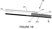
- Figure 1A illustrates a cross sectional view of a dual band antenna of a wireless electronic device, according to various embodiments of the present inventive concepts.
- Figures 1B illustrates a cross sectional view of the dual band antenna of Figure 1, according to various embodiments of the present inventive concepts.
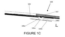
- Figures 1C illustrates a cross sectional views of the dual band antenna of Figure 1, according to various embodiments of the present inventive concepts.
- Figure 2 illustrates a plan view of the dual band antenna of Figures 1A-1C, according to various embodiments of the present inventive concepts.
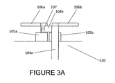
- Figure 3A illustrates a plan view of lowband dipole antenna strips of a dual band antenna of Figures 1A-2, according to various embodiments of the present inventive concepts.
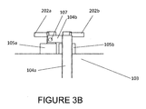
- Figure 3B illustrates a plan view of highband dipole antenna strips of a dual band antenna of Figures 1A-2, according to various embodiments of the present inventive concepts.
- Figure 4A illustrates a plan view of a first conductive layer of the dual band antenna of Figures 1A-3B, according to various embodiments of the present inventive concepts.
- Figure 4B illustrates a plan view of a third conductive layer of the dual band antenna of Figures 1A-3B, according to various embodiments of the present inventive concepts.
- Figure 4C illustrates a plan view of a second conductive layer of the dual band antenna of Figures 1A-3B, according to various embodiments of the present inventive concepts.
- Figures 5A graphically illustrates the frequency response of the antenna of Figures 1A-4C, according to various embodiments of the present inventive concepts.
- Figure 5B illustrates the lowband radiation pattern for the antenna of Figures 2-4C, according to various embodiments of the present inventive concepts.
- Figures 6A graphically illustrates the frequency response of the antenna of Figures 1A-4C, according to various embodiments of the present inventive concepts.
- Figures 6B illustrates the highband radiation pattern at point 1 of Figure 6A according to various embodiments of the present inventive concepts.
- Figures 6C illustrates the highband radiation pattern at point 2 of Figure 6A according to various embodiments of the present inventive concepts.
- Figures 6D illustrates the highband radiation pattern at point 3 of Figure 6A according to various embodiments of the present inventive concepts.
- spatially relative terms such as “above,” “below,” “upper,” “lower,” “top,” “bottom,” and the like, may be used herein for ease of description to describe one element or feature's relationship to another element(s) or feature(s) as illustrated in the figures. It will be understood that the spatially relative terms are intended to encompass different orientations of the device in use or operation in addition to the orientation depicted in the figures. For example, if the device in the figures is turned over, elements described as “below” other elements or features would then be oriented “above” the other elements or features. Thus, the term “below” can encompass both an orientation of above and below. The device may be otherwise oriented (rotated 90 degrees or at other orientations) and the spatially relative descriptors used herein interpreted accordingly. Well-known functions or constructions may not be described in detail for brevity and/or clarity.
- Antennas are commonly used in microwave antenna designs for wireless electronic devices such as mobile terminals including smart phones and tablets. These antenna designs may be compact in size and easy to manufacture since they may be implemented as printed features on printed circuit boards (PCBs). Various wireless communication applications may use these printed antenna designs.
- PCBs printed circuit boards
- Various wireless communication applications may use these printed antenna designs.
- a disadvantage of many printed antenna designs is that they achieve resonance at a single resonant frequency.
- these single resonant antennas may narrow the radiation pattern into a beam that is directional and may require the device to be directed towards a base station.
- these single resonant frequency antennas may produce irregular radiation patterns that are not suitable for extremely high frequency (EHF) radio antenna applications such as millimeter wave antenna arrays for use in the 10 to 300 GHz frequency range.
- EHF extremely high frequency
- the extremely high frequencies may be used for various types of communication in smart phones such as broadband internet access, Wi-Fi, etc. It may be desired to build a single antenna with a dual band multilayer printed dipole with an integrated balun to achieve multiple resonant frequencies for use in multiple applications for mobile phones using multiple EHF resonant frequencies.
- a dual band printed antenna may be implemented using three conductive layers of a PCB to include a stripline, lowband antenna arms, and highband antenna arms on different layers of the PCB.
- the dual band antenna with three layers may exhibit good polarization characteristics with a broad radiation beam that is substantially symmetric with wide scanning angles at both lowband and highband frequencies.
- the wireless electronic device 100 may include multiple conductive layers 101 separated by dielectric layers 102a and/or 102b. These conductive layers may include a suitable conductor such as copper.
- wireless electronic device 100 may include a first conductive layer 101a, a second conductive layer 101b, and a third conductive layer 101c.
- the dielectric layers 102a and/or 102b may include a material with a high dielectric constant and a low dissipation factor tan ⁇ .
- a ground plane 103 may be included on at least a portion of the second conductive layer 101b.
- Dielectric layers 102a and/or 102b may be between various conductive layers.
- a feeding via 107 may extend through dielectric layer 102a and electrically connect a stripline 104 to the balun (not shown).
- a current phase controlling element 105 may include two portions 105a and 105b that are separated by a slot therebetween.
- the wireless electronic device 100 may include one or more antenna element vias 108a and/or 108b that may electrically connect the current phase controlling element 105 to at least one or more lowband dipole antenna strips 106a and/or 106b through the second dielectric layer 102b.
- a portion 104b of the stripline 104 may be included in the balun 201.
- the stripline 104 may be connect by the feeding via 107 to one or more highband dipole antenna strips 202a and/or 202b.
- the stripline 104 may be in a different conductive layer from the ground plane 103.
- the stripline 104 may be on a first conductive layer 101a and the ground plane 103 may be on a second conductive layer 101b.
- a balun structure 201 may include the ground plane 103, a current phase controlling element 105, and a feeding via 107.
- the current phase controlling element 105 may include a first portion 105a and a second portion 105b with a slot therebetween. The width of the slot, i.e. the distance between the first portion 105a and the second portion 105b of the current phase controlling element 105, may control the phase of the current of the wireless electronic device 100.
- the wireless electronic device 100 may include lowband dipole antenna strips 106a and/or 106b.
- the wireless electronic device 100 may be configured to resonate at two resonant frequencies when excited by a signal transmitted and/or received through the stripline 104.
- the two resonant frequencies may include a lowband resonant frequency and/or a highband resonant frequency.
- the ground plane 103 may be spaced apart from the lowband dipole antenna strips 106a and/or 106b and/or spaced apart from the highband dipole antenna strips 202a and/or 202b by a length L.
- the length L may be in the range of 0.125 wavelength to 0.5 wavelength of the lowband resonant frequency and/or a highband resonant frequency. In some embodiments, the length L may be approximately 0.25 wavelength of the lowband resonant frequency and/or a highband resonant frequency.
- a first portion of the stripline 104a may overlap the second portion of the current phase controlling element 105b for electromagnetic coupling to form an electromagnetic radiation pattern.
- the thickness of the dielectric layer 102a of Figure 1A may affect the selection of the width of the first portion of the stripline 104a. It may be desired for stripline 104 to be impedance matched to the balun 201 of Figure 2. In some embodiments, the width of the stripline is based on a thickness of the first dielectric layer between the first and second conductive layers.
- the stripline 104 may be positioned to impedance match the balun 201.
- the first portion of the stripline 104a may overlap the second portion of the current phase controlling element 105b to produce electromagnetic coupling such that the lowband dipole antenna strips 106a and/or 106b resonate at a lowband resonant frequency.
- the lowband resonant frequency may be in the extremely high frequency (EHF) for radio antenna applications such as millimeter wave antennas for use in the 10 to 300 GHz frequency range.
- the length of one of the lowband dipole antenna strips 106a and/or 106b may be approximately 0.25 wavelengths of the lowband resonant frequency. In some embodiments, the length of one of the lowband dipole antenna strips 106a and/or 106b may be in the range of 0.125 wavelength to 0.5 wavelength of the lowband resonant frequency.
- the feeding via 107 may electrically connect the stripline 104b with at least one of the highband dipole antenna strips 202a and/or 202b.
- the first portion of the stripline 104a may overlap the second portion of the current phase controlling element 105b to produce magnetic coupling such that the highband dipole antenna strips 202a and/or 202b resonate at a highband resonant frequency.
- the highband resonant frequency may be in the extremely high frequency (EHF) range of 10 to 300 GHz.
- the length of one of the highband dipole antenna strips 202a and/or 202b may be approximately 0.25 wavelengths of the highband resonant frequency. In some embodiments, the length of one of the highband dipole antenna strips 202a and/or 202b may be in the range of 0.125 wavelength to 0.5 wavelength of the highband resonant frequency.
- FIG. 4A a plan view of the first conductive layer 101a of Figure 1A is illustrated.
- a stripline 104 may be included in layer 101a.
- a feeding via 107 may extend from the stripline 104 in the first conductive layer 101a to a highband dipole antenna strips 202a and/or 202b in the second conductive layer 101b.
- the dotted line marks an edge of the ground plane 103 in the second conductive layer 101b.
- the third conductive layer 101c may be on the bottom of the wireless electronic device 100.
- an antenna element via 108a and/or 108b may extend through dielectric layer 102b from the current phase controller element 105a and/or 105b in the second conductive layer 101b to the lowband dipole antenna strips 106a and/or 106b in the third conductive layer 101c.
- the antenna element via 108a and/or 108b may electrically connect the current phase controller element 105a and/or 105b with the lowband dipole antenna strips 106a and/or 106b.
- FIG. 4C a plan view of the second conductive layer 101b of Figure 1A is illustrated.
- the ground plane 103, the current phase controller elements 105a and 105b, and/or the highband dipole antenna strips 202a and/or 202b may be located in the second conductive layer 101b.
- a feeding via 107 may extend though dielectric layer 102a from the stripline 104 in the first conductive layer 101a to the highband dipole antenna strips 202a and/or 202b in the second conductive layer 101b.
- An antenna element via 108a and/or 108b may extend through dielectric layer 102b from the current phase controller 105a and/or 105b in the second conductive layer 101b to the lowband dipole antenna strips 106a and/or 106b in the third conductive layer 101c.
- FIG. 5A an example frequency response of the wireless electronic device 100 of Figures 1A-4C is illustrated.
- Figure 5A graphically illustrates both a lowband resonant frequency and a highband resonant frequency.
- the frequency response at point 1 has a lowband resonant frequency of approximately 16GHz.
- the -10 dB bandwidth around this lowband resonant frequency may be 1100MHz, which may be approximately 7.3% of the lowband resonant frequency.
- the frequency response around the lowband resonant frequency produces a wide bandwidth response around the lowband resonant frequency.
- the radiation pattern for the antenna of Figures 1A-4C is illustrated, with a lowband resonant frequency of approximately 16GHz is illustrated.
- the radiation pattern around 16GHz spans broadly and uniformly around the top edge of the device 100 with few prominent side lobes and little distortion.
- Figure 6A the frequency response of the antenna of Figures 1A-4C is illustrated.
- Figure 6A graphically illustrates both a lowband resonant frequency and a highband resonant frequency.
- the antenna of Figures 1A-4C is designed to have a highband resonant frequency response near 30GHz.
- the -10 dB bandwidth around this lowband resonant frequency may be 11.5 GHz, which may be approximately 33% of the highband resonant frequency.
- This very wide bandwidth provided by this antenna around the highband resonant frequency offers excellent signal integrity with potential for use at several different frequencies in this bandwidth range.
- the radiation patterns at points 1, 2, and 3 respectively of Figure 6A is illustrated.
- this antenna may be primarily for use as a dual band antenna, the wideband radiation patterns at these additional frequencies provide potential for use of the antenna at one or more additional frequencies in addition to the primary lowband and highband frequencies described herein. Accordingly, the antenna design described herein may provide excellent performance at several frequencies for a variety of extremely high frequencies.
- Electromagnetic properties of the described antenna structures may be determined by physical dimensions and other parameters. For example, parameters such as stripline width, stripline positioning, dielectric layer thickness, dielectric layer permittivity, and length of antenna arms, may affect the electromagnetic properties of antenna structures and subsequently the antenna performance.
- the dual band dipole antenna may provide, for example, antenna coverage in the 15 GHz band and the 28-35 GHz band. Both bands provide omnidirectional patterns and may be used in antenna array applications. These structures may be easily integrated into multilayer PCB structures and may be cost efficient to manufacture.
- the integrated balun may be repeated in an array pattern and configured to receive and/or transmit multiple-input and multiple-output (MIMO) communication and/or 3D MIMO communication. Respective radiation fields formed by the integrated balun structures may additively couple to form an electromagnetic radiation beam for beamforming applications.
- MIMO multiple-input and multiple-output
Abstract
A wireless electronic device includes a printed circuit board (PCB) with first, second, and third conductive layers separated from one another by dielectric layers. A stripline is included in the first conductive layer. Two highband dipole antenna strips are included in the second conductive layer and/or two lowband dipole antenna strips are included in the third conductive layer. The wireless electronic device may be configured to resonate at a lowband resonant frequency corresponding to the two lowband dipole antenna strips and resonate at a highband resonant frequency corresponding to the two highband dipole antenna strips when excited by a signal transmitted and/or received though the stripline.
Description
The present inventive concepts generally relate to the field wireless communications and, more specifically, to antennas for wireless communication devices.
CROSS REFERENCE TO RELATED APPLICATIONS
This application claims priority from US patent application No. 14/549,547, filed November 21, 2014, the entire disclosure of which hereby is incorporated by reference.
This application claims priority from US patent application No. 14/549,547, filed November 21, 2014, the entire disclosure of which hereby is incorporated by reference.
Communication devices such as cell phones and other user equipment may include antennas that can be used to communicate with external devices. These antennas designs may operate at multiple resonant frequencies. Some antenna designs, however, may not provide suitable performance of the antenna.
Various embodiments of the present inventive concepts include a wireless electronic device including a printed circuit board (PCB) with first, second, and third conductive layers separated from one another by dielectric layers. A stripline may be included in the first conductive layer. Two highband dipole antenna strips may be included in the second conductive layer and/or two lowband dipole antenna strips may be included in the third conductive layer. The wireless electronic device may be configured to resonate at a lowband resonant frequency corresponding to the two lowband dipole antenna strips and response at a highband resonant frequency corresponding to the two highband dipole antenna strips when excited by a signal transmitted and/or received though the stripline. In some embodiments, the wireless electronic device may include a feeding via that electrically connects the stripline to at least one of the highband dipole antenna strips through the first dielectric layer.
According to some embodiments, the wireless electronic device may include a balun. The balun may include a ground plane and/or a current phase controlling element. The ground plane and the current phase controlling element may be in the second conductive layer. The current phase controlling element may include a first portion and a second portion with a slot therebetween. The width of the slot may control the phase of the current of the wireless electronic device.
According to some embodiments, the stripline may include a first portion and a second portion. The first portion of the stripline may be positioned to overlap the second portion of the current phase controlling element for electromagnetic coupling to form an electromagnetic radiation beam. In some embodiments, a feeding via may electrically connect the second portion of the stripline to at least one of the highband dipole antenna strips. In some embodiments, the wireless electronic device may include an antenna element via that electrically connects the current phase controlling element to at least one of the lowband dipole antenna strips through the second dielectric layer.
According to some embodiments, the two resonant frequencies of the wireless electronic device may include a lowband resonant frequency and a highband resonant frequency. The lowband dipole antenna strips may be configured to resonate at the lowband resonant frequency, and/or the highband dipole antenna strips may be configured to resonate at the highband resonant frequency. A length of one of the lowband dipole antenna strips may be approximately 0.25 wavelengths of the lowband frequency, and/or a length of one of the highband dipole antenna strips may be approximately 0.25 wavelengths of the highband resonant frequency. The stripline may be positioned to impedance match the balun. The width of the stripline may be based on a thickness of the first dielectric layer between the first and second conductive layers.
Various embodiments of the present inventive concepts include a wireless electronic device including a printed circuit board (PCB) with first, second, and third layers separated from one another by dielectric layers. The wireless electronic device may include a stripline in a first layer, a current phase controlling element in a second layer, two highband dipole antenna strips in the second layer and/or two lowband dipole antenna strips in a third layer. An antenna element via may extend from the current phase controlling element in the second layer to at least one of the lowband dipole antenna strips in the third layer. A feeding via may extend from the stripline in the first layer to at least one of the highband dipole antenna strips in the second layer.
Other devices and/or operations according to embodiments of the inventive concept will be or become apparent to one with skill in the art upon review of the following drawings and detailed description. It is intended that all such additional devices and/or operations be included within this description, be within the scope of the present inventive concept, and be protected by the accompanying claims. Moreover, it is intended that all embodiments disclosed herein can be implemented separately or combined in any way and/or combination.
The present inventive concepts now will be described more fully with reference to the accompanying drawings, in which embodiments of the inventive concepts are shown. However, the present application should not be construed as limited to the embodiments set forth herein. Rather, these embodiments are provided so that this disclosure will be thorough and complete, and to fully convey the scope of the embodiments to those skilled in the art. Like reference numbers refer to like elements throughout.
The terminology used herein is for the purpose of describing particular embodiments only and is not intended to be limiting of the embodiments. As used herein, the singular forms "a," "an," and "the" are intended to include the plural forms as well, unless the context clearly indicates otherwise. It will be further understood that the terms "comprises," "comprising," "includes," and/or "including," (and variants thereof) when used herein, specify the presence of stated features, steps, operations, elements, and/or components, but do not preclude the presence or addition of one or more other features, steps, operations, elements, components, and/or groups thereof. In contrast, the term "consisting of" (and variants thereof) when used herein, specifies the stated features, integers, steps, operations, elements, and/or components, and precludes additional features, integers, steps, operations, elements and/or components.
It will be understood that when an element is referred to as being "coupled," "connected," or "responsive" to another element, it can be directly coupled, connected, or responsive to the other element, or intervening elements may also be present. In contrast, when an element is referred to as being "directly coupled," "directly connected," or "directly responsive" to another element, there are no intervening elements present. As used herein, the term "and/or" includes any and all combinations of one or more of the associated listed items.
Spatially relative terms, such as "above," "below," "upper," "lower," "top," "bottom," and the like, may be used herein for ease of description to describe one element or feature's relationship to another element(s) or feature(s) as illustrated in the figures. It will be understood that the spatially relative terms are intended to encompass different orientations of the device in use or operation in addition to the orientation depicted in the figures. For example, if the device in the figures is turned over, elements described as "below" other elements or features would then be oriented "above" the other elements or features. Thus, the term "below" can encompass both an orientation of above and below. The device may be otherwise oriented (rotated 90 degrees or at other orientations) and the spatially relative descriptors used herein interpreted accordingly. Well-known functions or constructions may not be described in detail for brevity and/or clarity.
It will be understood that, although the terms "first," "second," etc. may be used herein to describe various elements, these elements should not be limited by these terms. These terms are only used to distinguish one element from another. Thus, a first element could be termed a second element without departing from the teachings of the present embodiments.
Unless otherwise defined, all terms (including technical and scientific terms) used herein have the same meaning as commonly understood by one of ordinary skill in the art to which these embodiments belong. It will be further understood that terms, such as those defined in commonly-used dictionaries, should be interpreted as having a meaning that is consistent with their meaning in the context of the relevant art and will not be interpreted in an idealized or overly-formal sense unless expressly so defined herein.
Antennas are commonly used in microwave antenna designs for wireless electronic devices such as mobile terminals including smart phones and tablets. These antenna designs may be compact in size and easy to manufacture since they may be implemented as printed features on printed circuit boards (PCBs). Various wireless communication applications may use these printed antenna designs. However, a disadvantage of many printed antenna designs is that they achieve resonance at a single resonant frequency. Moreover, these single resonant antennas may narrow the radiation pattern into a beam that is directional and may require the device to be directed towards a base station. Furthermore, these single resonant frequency antennas may produce irregular radiation patterns that are not suitable for extremely high frequency (EHF) radio antenna applications such as millimeter wave antenna arrays for use in the 10 to 300 GHz frequency range. The extremely high frequencies may be used for various types of communication in smart phones such as broadband internet access, Wi-Fi, etc. It may be desired to build a single antenna with a dual band multilayer printed dipole with an integrated balun to achieve multiple resonant frequencies for use in multiple applications for mobile phones using multiple EHF resonant frequencies.
According to various embodiments of the present inventive concepts, a dual band printed antenna may be implemented using three conductive layers of a PCB to include a stripline, lowband antenna arms, and highband antenna arms on different layers of the PCB. The dual band antenna with three layers may exhibit good polarization characteristics with a broad radiation beam that is substantially symmetric with wide scanning angles at both lowband and highband frequencies.
Referring now to Figure 1A, a side view of the wireless electronic device 100 is illustrated. The wireless electronic device 100 may include multiple conductive layers 101 separated by dielectric layers 102a and/or 102b. These conductive layers may include a suitable conductor such as copper. For example, wireless electronic device 100 may include a first conductive layer 101a, a second conductive layer 101b, and a third conductive layer 101c. The dielectric layers 102a and/or 102b may include a material with a high dielectric constant and a low dissipation factor tan δ. For example, a material such as Rogers RO4003C may be used as the dielectric layers 102, such that the dielectric constant Er (epsilon)= 3.55 and the dissipation factor tan δ = 0.0027 at 10 GHz.
Referring to Figure 1B, a ground plane 103 may be included on at least a portion of the second conductive layer 101b. Dielectric layers 102a and/or 102b may be between various conductive layers. A feeding via 107 may extend through dielectric layer 102a and electrically connect a stripline 104 to the balun (not shown). A current phase controlling element 105 may include two portions 105a and 105b that are separated by a slot therebetween.
Referring to Figure 1C, the wireless electronic device 100 may include one or more antenna element vias 108a and/or 108b that may electrically connect the current phase controlling element 105 to at least one or more lowband dipole antenna strips 106a and/or 106b through the second dielectric layer 102b.
Referring to Figure 2, in some embodiments, a portion 104b of the stripline 104 may be included in the balun 201. The stripline 104 may be connect by the feeding via 107 to one or more highband dipole antenna strips 202a and/or 202b. The stripline 104 may be in a different conductive layer from the ground plane 103. For example, the stripline 104 may be on a first conductive layer 101a and the ground plane 103 may be on a second conductive layer 101b. A balun structure 201 may include the ground plane 103, a current phase controlling element 105, and a feeding via 107. The current phase controlling element 105 may include a first portion 105a and a second portion 105b with a slot therebetween. The width of the slot, i.e. the distance between the first portion 105a and the second portion 105b of the current phase controlling element 105, may control the phase of the current of the wireless electronic device 100.
Still referring to Figure 2, the wireless electronic device 100 may include lowband dipole antenna strips 106a and/or 106b. The wireless electronic device 100 may be configured to resonate at two resonant frequencies when excited by a signal transmitted and/or received through the stripline 104. The two resonant frequencies may include a lowband resonant frequency and/or a highband resonant frequency. The ground plane 103 may be spaced apart from the lowband dipole antenna strips 106a and/or 106b and/or spaced apart from the highband dipole antenna strips 202a and/or 202b by a length L. In some embodiments, the length L may be in the range of 0.125 wavelength to 0.5 wavelength of the lowband resonant frequency and/or a highband resonant frequency. In some embodiments, the length L may be approximately 0.25 wavelength of the lowband resonant frequency and/or a highband resonant frequency.
Referring to Figure 3A, the antenna of Figure 2 with lowband dipole antenna strips 106a and/or 106b is illustrated. A first portion of the stripline 104a may overlap the second portion of the current phase controlling element 105b for electromagnetic coupling to form an electromagnetic radiation pattern. The thickness of the dielectric layer 102a of Figure 1A may affect the selection of the width of the first portion of the stripline 104a. It may be desired for stripline 104 to be impedance matched to the balun 201 of Figure 2. In some embodiments, the width of the stripline is based on a thickness of the first dielectric layer between the first and second conductive layers.
Still referring to Figure 3A, the stripline 104 may be positioned to impedance match the balun 201. The first portion of the stripline 104a may overlap the second portion of the current phase controlling element 105b to produce electromagnetic coupling such that the lowband dipole antenna strips 106a and/or 106b resonate at a lowband resonant frequency. The lowband resonant frequency may be in the extremely high frequency (EHF) for radio antenna applications such as millimeter wave antennas for use in the 10 to 300 GHz frequency range. The length of one of the lowband dipole antenna strips 106a and/or 106b may be approximately 0.25 wavelengths of the lowband resonant frequency. In some embodiments, the length of one of the lowband dipole antenna strips 106a and/or 106b may be in the range of 0.125 wavelength to 0.5 wavelength of the lowband resonant frequency.
Referring to Figure 3B, the antenna of Figure 2 with highband dipole antenna strips 202a and/or 202b is illustrated. The feeding via 107 may electrically connect the stripline 104b with at least one of the highband dipole antenna strips 202a and/or 202b. The first portion of the stripline 104a may overlap the second portion of the current phase controlling element 105b to produce magnetic coupling such that the highband dipole antenna strips 202a and/or 202b resonate at a highband resonant frequency. The highband resonant frequency may be in the extremely high frequency (EHF) range of 10 to 300 GHz. The length of one of the highband dipole antenna strips 202a and/or 202b may be approximately 0.25 wavelengths of the highband resonant frequency. In some embodiments, the length of one of the highband dipole antenna strips 202a and/or 202b may be in the range of 0.125 wavelength to 0.5 wavelength of the highband resonant frequency.
Referring to Figure 4A, a plan view of the first conductive layer 101a of Figure 1A is illustrated. A stripline 104 may be included in layer 101a. A feeding via 107 may extend from the stripline 104 in the first conductive layer 101a to a highband dipole antenna strips 202a and/or 202b in the second conductive layer 101b. The dotted line marks an edge of the ground plane 103 in the second conductive layer 101b.
Referring to Figure 4B, a plan view of the third conductive layer 101c of Figure 1A is illustrated. In some embodiments, the third conductive layer 101c may be on the bottom of the wireless electronic device 100. In some embodiments, an antenna element via 108a and/or 108b may extend through dielectric layer 102b from the current phase controller element 105a and/or 105b in the second conductive layer 101b to the lowband dipole antenna strips 106a and/or 106b in the third conductive layer 101c. The antenna element via 108a and/or 108b may electrically connect the current phase controller element 105a and/or 105b with the lowband dipole antenna strips 106a and/or 106b.
Referring to Figure 4C, a plan view of the second conductive layer 101b of Figure 1A is illustrated. In some embodiments, the ground plane 103, the current phase controller elements 105a and 105b, and/or the highband dipole antenna strips 202a and/or 202b may be located in the second conductive layer 101b. A feeding via 107 may extend though dielectric layer 102a from the stripline 104 in the first conductive layer 101a to the highband dipole antenna strips 202a and/or 202b in the second conductive layer 101b. An antenna element via 108a and/or 108b may extend through dielectric layer 102b from the current phase controller 105a and/or 105b in the second conductive layer 101b to the lowband dipole antenna strips 106a and/or 106b in the third conductive layer 101c.
Referring to Figure 5A, an example frequency response of the wireless electronic device 100 of Figures 1A-4C is illustrated. Figure 5A graphically illustrates both a lowband resonant frequency and a highband resonant frequency. In this non-limiting example, the frequency response at point 1 has a lowband resonant frequency of approximately 16GHz. The -10 dB bandwidth around this lowband resonant frequency may be 1100MHz, which may be approximately 7.3% of the lowband resonant frequency. In other words, the frequency response around the lowband resonant frequency produces a wide bandwidth response around the lowband resonant frequency.
Referring to Figure 5B, the radiation pattern for the antenna of Figures 1A-4C, is illustrated, with a lowband resonant frequency of approximately 16GHz is illustrated. The radiation pattern around 16GHz spans broadly and uniformly around the top edge of the device 100 with few prominent side lobes and little distortion.
Referring to Figure 6A, the frequency response of the antenna of Figures 1A-4C is illustrated. Figure 6A graphically illustrates both a lowband resonant frequency and a highband resonant frequency. In this non-limiting example, the antenna of Figures 1A-4C is designed to have a highband resonant frequency response near 30GHz. The -10 dB bandwidth around this lowband resonant frequency may be 11.5 GHz, which may be approximately 33% of the highband resonant frequency. This very wide bandwidth provided by this antenna around the highband resonant frequency offers excellent signal integrity with potential for use at several different frequencies in this bandwidth range.
Referring to Figures 6B-6D, the radiation patterns at points 1, 2, and 3 respectively of Figure 6A is illustrated. The radiation patterns at approximately 30 GHz, 33GHz, and 36 GHz at points 1, 2, and 3 respectively, each span broadly and uniformly around the top edge of the wireless electronic device 100 with few prominent side lobes and little distortion. Although this antenna may be primarily for use as a dual band antenna, the wideband radiation patterns at these additional frequencies provide potential for use of the antenna at one or more additional frequencies in addition to the primary lowband and highband frequencies described herein. Accordingly, the antenna design described herein may provide excellent performance at several frequencies for a variety of extremely high frequencies.
Electromagnetic properties of the described antenna structures may be determined by physical dimensions and other parameters. For example, parameters such as stripline width, stripline positioning, dielectric layer thickness, dielectric layer permittivity, and length of antenna arms, may affect the electromagnetic properties of antenna structures and subsequently the antenna performance.
As described herein, applying an integrated balun in multilayer environment with a stripline results in a compact dual band dipole. The dual band dipole antenna may provide, for example, antenna coverage in the 15 GHz band and the 28-35 GHz band. Both bands provide omnidirectional patterns and may be used in antenna array applications. These structures may be easily integrated into multilayer PCB structures and may be cost efficient to manufacture. The integrated balun may be repeated in an array pattern and configured to receive and/or transmit multiple-input and multiple-output (MIMO) communication and/or 3D MIMO communication. Respective radiation fields formed by the integrated balun structures may additively couple to form an electromagnetic radiation beam for beamforming applications.
Many different embodiments have been disclosed herein, in connection with the above description and the drawings. It will be understood that it would be unduly repetitious and obfuscating to literally describe and illustrate every combination and subcombination of these embodiments. Accordingly, the present specification, including the drawings, shall be construed to constitute a complete written description of all combinations and subcombinations of the embodiments described herein, and of the manner and process of making and using them, and shall support claims to any such combination or subcombination.
In the drawings and specification, there have been disclosed various embodiments and, although specific terms are employed, they are used in a generic and descriptive sense only and not for purposes of limitation.
Claims (19)
- A wireless electronic device (100), comprising:
a printed circuit board (PCB) comprising first, second, and third conductive layers (101a-101c) separated from one another by first and second dielectric layers (102a-102c) respectively;
a stripline (104) in the first conductive layer (101a);
two highband dipole antenna strips (202a, 202b) in the second conductive layer (101b) ; and
two lowband dipole antenna strips (106a, 106b) in the third conductive layer (101c),
wherein the wireless electronic device (100) is configured to resonate at a lowband resonant frequency corresponding to the two lowband dipole antenna strips (106a, 106b) and resonate at a highband resonant frequency corresponding to the two highband dipole antenna strips (202a, 202b) when excited by a signal transmitted and/or received though the stripline (104). - The wireless electronic device (100) of Claim 1, further comprising a balun (201), wherein the balun (201) comprises:
a ground plane (103); and
a current phase controlling element (105). - The wireless electronic device (100) of Claim 1, further comprising:
a feeding via (107) that electrically connects the stripline (104) to at least one of the highband dipole antenna strips (202a, 202b) through the first dielectric layer (102a). - The wireless electronic device (100) of Claim 2, wherein the ground plane (103) and the current phase controlling element (105) are in the second conductive layer (101b).
- The wireless electronic device (100) of Claim 2, wherein the current phase controlling element (105) comprises a first portion (105a) and a second portion (105b) with a slot therebetween.
- The wireless electronic device (100) of Claim 5, wherein a width of the slot controls the phase of the current of the wireless electronic device (100).
- The wireless electronic device (100) of Claim 2,
wherein the stripline (104) comprises a first portion (104a) and a second portion (104b), and
wherein the first portion (104a) of the stripline (104) is positioned to overlap the second portion (105b) of the current phase controlling element (105) for electromagnetic coupling to form an electromagnetic radiation beam. - The wireless electronic device (100) of Claim 7, further comprising:
a feeding via (107) that electrically connects the second portion (104b) of the stripline (104) to at least one of the highband dipole antenna strips (202) through the first dielectric layer (102a). - The wireless electronic device (100) of Claim 2, further comprising:
an antenna element via (108a) that electrically connects the current phase controlling element (105) to at least one of the lowband dipole antenna strips (106) through the second dielectric layer (102b). - The wireless electronic device (100) of Claim 1,
wherein a length of one of the lowband dipole antenna strips (106) is approximately 0.25 wavelengths of the lowband resonant frequency, and
wherein a length of one of the highband dipole antenna strips (202) is approximately 0.25 wavelengths of the highband resonant frequency. - The wireless electronic device (100) of Claim 2, wherein the stripline (104) is positioned to impedance match the balun (201).
- The wireless electronic device (100) of Claim 1, wherein the width of the stripline (104) is based on a thickness of the first dielectric layer (102a) between the first and second conductive layers (101a, 101b).
- A wireless electronic device (100), comprising:
a printed circuit board (PCB) comprising first, second, and third layers separated from one another by first and second dielectric layers (102a, 102b) respectively;
a stripline (104) in the first layer;
a current phase controlling element (105) in the second layer;
two highband dipole antenna strips (202) in the second layer;
two lowband dipole antenna strips (106) in the third layer;
an antenna element via (108a) extending through the second dielectric layer (102b) from the current phase controlling element (105) in the second layer to at least one of the lowband dipole antenna strips (106) in the third layer; and
a feeding via (107) extending through the first dielectric layer (102a) from the stripline (104) in the first layer to at least one of the highband dipole antenna strips (202) in the second layer. - The wireless electronic device (100) of Claim 13, further comprising a ground plane (103) in the second layer.
- The wireless electronic device (100) of Claim 13, wherein the current phase controlling element (105) comprises a first portion (105a) and a second portion (105b) with a slot therebetween.
- The wireless electronic device (100) of Claim 15, wherein a width of the slot controls the phase of the current of the wireless electronic device (100).
- The wireless electronic device (100) of Claim 13,
wherein the stripline (104) comprises a first portion (104a) and a second portion (104b), and
wherein the first portion (104a) of the stripline (104) is positioned to overlap the second portion (105b) of the current phase controlling element (105) for electromagnetic coupling to form an electromagnetic radiation beam. - The wireless electronic device (100) of Claim 13,
wherein the wireless electronic device (100) is configured to resonate at a lowband resonant frequency corresponding to the two lowband dipole antenna strips (106) and resonate at a highband resonant frequency corresponding to the two highband dipole antenna strips (202) when excited by a signal transmitted and/or received though the stripline (104). - The wireless electronic device (100) of Claim 18,
wherein a length of one of the lowband dipole antenna strips (106) is approximately 0.25 wavelengths of the lowband resonant frequency, and
wherein a length of one of the highband dipole antenna strips (202) is approximately 0.25 wavelengths of the highband resonant frequency.
Priority Applications (2)
| Application Number | Priority Date | Filing Date | Title |
|---|---|---|---|
| EP15726358.3A EP3221926B1 (en) | 2014-11-21 | 2015-05-20 | Dual band multi-layer dipole antennas for wireless electronic devices |
| CN201580053392.0A CN107078393B (en) | 2014-11-21 | 2015-05-20 | Wireless electronic device |
Applications Claiming Priority (2)
| Application Number | Priority Date | Filing Date | Title |
|---|---|---|---|
| US14/549,574 US9496623B2 (en) | 2014-11-21 | 2014-11-21 | Dual band multi-layer dipole antennas for wireless electronic devices |
| US14/549,574 | 2014-11-21 |
Publications (1)
| Publication Number | Publication Date |
|---|---|
| WO2016079902A1 true WO2016079902A1 (en) | 2016-05-26 |
Family
ID=56011135
Family Applications (1)
| Application Number | Title | Priority Date | Filing Date |
|---|---|---|---|
| PCT/JP2015/002548 WO2016079902A1 (en) | 2014-11-21 | 2015-05-20 | Dual band multi-layer dipole antennas for wireless electronic devices |
Country Status (4)
| Country | Link |
|---|---|
| US (1) | US9496623B2 (en) |
| EP (1) | EP3221926B1 (en) |
| CN (1) | CN107078393B (en) |
| WO (1) | WO2016079902A1 (en) |
Cited By (1)
| Publication number | Priority date | Publication date | Assignee | Title |
|---|---|---|---|---|
| CN113708060A (en) * | 2021-08-16 | 2021-11-26 | 中国电子科技集团公司第四十三研究所 | Dipole antenna based on three-dimensional differential feed structure |
Families Citing this family (5)
| Publication number | Priority date | Publication date | Assignee | Title |
|---|---|---|---|---|
| WO2018213620A1 (en) * | 2017-05-18 | 2018-11-22 | John Mezzalingua Associates, LLC | Multi-band fast roll off antenna having multi-layer pcb-formed cloaked dipoles |
| CN110233360B (en) * | 2019-04-23 | 2020-10-16 | 中天宽带技术有限公司 | Dual-band antenna and electronic equipment |
| CN110148828B (en) * | 2019-05-22 | 2021-06-04 | 维沃移动通信有限公司 | Antenna unit and electronic device |
| CA3151711C (en) * | 2019-09-18 | 2023-11-21 | Huawei Technologies Co., Ltd. | Beam diversity by smart antenna with passive elements |
| CN114843763B (en) * | 2022-04-28 | 2023-06-27 | 安徽大学 | Lateral radiation grid array antenna based on multilayer PCB structure |
Citations (5)
| Publication number | Priority date | Publication date | Assignee | Title |
|---|---|---|---|---|
| US4825220A (en) * | 1986-11-26 | 1989-04-25 | General Electric Company | Microstrip fed printed dipole with an integral balun |
| US5532708A (en) * | 1995-03-03 | 1996-07-02 | Motorola, Inc. | Single compact dual mode antenna |
| US20040036655A1 (en) * | 2002-08-22 | 2004-02-26 | Robert Sainati | Multi-layer antenna structure |
| EP1687867A1 (en) * | 2003-11-24 | 2006-08-09 | Sandbridge Technologies, Inc. | Modified printed dipole antennas for wireless multi-band communication systems |
| US20080030418A1 (en) * | 2005-02-18 | 2008-02-07 | Patrice Brachat | Multi-band printed dipole antenna |
Family Cites Families (8)
| Publication number | Priority date | Publication date | Assignee | Title |
|---|---|---|---|---|
| US5274391A (en) * | 1990-10-25 | 1993-12-28 | Radio Frequency Systems, Inc. | Broadband directional antenna having binary feed network with microstrip transmission line |
| US6720934B1 (en) * | 2001-01-25 | 2004-04-13 | Skywire Broadband, Inc. | Parallel fed collinear dipole array antenna |
| US7075493B2 (en) * | 2002-05-01 | 2006-07-11 | The Regents Of The University Of Michigan | Slot antenna |
| US7688267B2 (en) * | 2006-11-06 | 2010-03-30 | Apple Inc. | Broadband antenna with coupled feed for handheld electronic devices |
| CN101542833B (en) * | 2007-01-11 | 2012-07-04 | 松下电器产业株式会社 | Wide-band slot antenna |
| JP4904197B2 (en) * | 2007-05-08 | 2012-03-28 | パナソニック株式会社 | Unbalanced feed broadband slot antenna |
| WO2010036955A1 (en) * | 2008-09-25 | 2010-04-01 | Pinyon Technologies, Inc. | Slot antennas, including meander slot antennas, and use of same in current fed and phased array configurations |
| US8368602B2 (en) * | 2010-06-03 | 2013-02-05 | Apple Inc. | Parallel-fed equal current density dipole antenna |
-
2014
- 2014-11-21 US US14/549,574 patent/US9496623B2/en active Active
-
2015
- 2015-05-20 EP EP15726358.3A patent/EP3221926B1/en active Active
- 2015-05-20 CN CN201580053392.0A patent/CN107078393B/en active Active
- 2015-05-20 WO PCT/JP2015/002548 patent/WO2016079902A1/en active Application Filing
Patent Citations (5)
| Publication number | Priority date | Publication date | Assignee | Title |
|---|---|---|---|---|
| US4825220A (en) * | 1986-11-26 | 1989-04-25 | General Electric Company | Microstrip fed printed dipole with an integral balun |
| US5532708A (en) * | 1995-03-03 | 1996-07-02 | Motorola, Inc. | Single compact dual mode antenna |
| US20040036655A1 (en) * | 2002-08-22 | 2004-02-26 | Robert Sainati | Multi-layer antenna structure |
| EP1687867A1 (en) * | 2003-11-24 | 2006-08-09 | Sandbridge Technologies, Inc. | Modified printed dipole antennas for wireless multi-band communication systems |
| US20080030418A1 (en) * | 2005-02-18 | 2008-02-07 | Patrice Brachat | Multi-band printed dipole antenna |
Cited By (1)
| Publication number | Priority date | Publication date | Assignee | Title |
|---|---|---|---|---|
| CN113708060A (en) * | 2021-08-16 | 2021-11-26 | 中国电子科技集团公司第四十三研究所 | Dipole antenna based on three-dimensional differential feed structure |
Also Published As
| Publication number | Publication date |
|---|---|
| CN107078393B (en) | 2020-12-25 |
| US20160149314A1 (en) | 2016-05-26 |
| EP3221926B1 (en) | 2020-07-22 |
| EP3221926A1 (en) | 2017-09-27 |
| US9496623B2 (en) | 2016-11-15 |
| CN107078393A (en) | 2017-08-18 |
Similar Documents
| Publication | Publication Date | Title |
|---|---|---|
| US10854994B2 (en) | Broadband phased array antenna system with hybrid radiating elements | |
| US10224622B2 (en) | Antennas including dual radiating elements for wireless electronic devices | |
| EP3189560B1 (en) | Reconfigurable multi-band antenna with four to ten ports | |
| EP3221926B1 (en) | Dual band multi-layer dipole antennas for wireless electronic devices | |
| Lim et al. | Monopole-like and boresight pattern reconfigurable antenna | |
| US9711860B2 (en) | Wideband antennas including a substrate integrated waveguide | |
| US10103440B2 (en) | Stripline coupled antenna with periodic slots for wireless electronic devices | |
| WO2016097712A1 (en) | Reconfigurable multi-band multi-function antenna | |
| US11063350B2 (en) | Edge enabled void antenna apparatus | |
| EP3245690B1 (en) | Dual-band inverted-f antenna with multiple wave traps for wireless electronic devices | |
| EP3213372B1 (en) | Inverted-f antenna with a choke notch for wireless electronic devices | |
| CN116868442A (en) | Low profile device including coupled resonant structure layers | |
| KR101096461B1 (en) | Monopole Chip Antenna using Ground Path in 2.4GHz | |
| Zaid et al. | Miniaturized microstrip patch antenna using magneto-dielectric substrate for RFID applications | |
| Real et al. | Phased array antennas for mmWave frequency spectrum for 5G communication | |
| Van Trinh et al. | Internal Reconfigurable Dipole–Loop Antenna Array for High Reception Rate of Wideband UHD-TV Applications | |
| CN107210517B (en) | Wireless electron device | |
| CN113131204A (en) | Circularly polarized antenna |
Legal Events
| Date | Code | Title | Description |
|---|---|---|---|
| 121 | Ep: the epo has been informed by wipo that ep was designated in this application |
Ref document number: 15726358 Country of ref document: EP Kind code of ref document: A1 |
|
| REEP | Request for entry into the european phase |
Ref document number: 2015726358 Country of ref document: EP |
|
| NENP | Non-entry into the national phase |
Ref country code: DE |